Article

Experimental Validation of Metaheuristic and Conventional Modulation, and Hysteresis Control of the Dual Boost Nine-Level Inverter

1
Department of Electrical Engineering, Zakir Husain College of Engineering & Technology, Aligarh Muslim University, Aligarh 202002, Uttar Pradesh, India
2
School of Engineering and Information Technology, University of New South Wales, Canberra at ADFA, Canberra, BC 2610, Australia
*
Authors to whom correspondence should be addressed.
Electronics 2021, 10(2), 207; https://doi.org/10.3390/electronics10020207
Submission received: 13 December 2020 / Revised: 27 December 2020 / Accepted: 30 December 2020 / Published: 18 January 2021
(This article belongs to the Section Industrial Electronics)

Abstract

:
In this article, various modulation strategies and hysteresis-band control of a recently introduced dual-boost nine-level inverter (DB9LI) are implemented. DB9LI is a switched capacitor based inverter capable of generating symmetrical nine output voltage levels by employing a single DC source. The topology generates a boosted bipolar voltage at the output side without applying end-side H-bridge (usually employed to generate negative levels), which contrasts with some of the switched-capacitor topologies. The capacitors employed have an inherent self-balancing feature. Additionally, due to lower individual and total standing voltages, switches of low voltage ratings are required. As a result, the cost of switches and the inverter reduces considerably. Metaheuristic-based selective harmonic elimination and mitigation (SHE and SHM) and various sine-triangular pulse width modulation techniques are implemented and compared on various parameters. Finally, a robust eight-band hysteresis control is designed and implemented, which helps to obtain sinusoidal load current with a unity power factor. The modulation strategies and the hysteresis control are validated on the MATLAB simulation environment and an experimental prototype.

1. Introduction

Multilevel Inverters (MLIs) in the last few decades have emerged as convincing power converter technology in a multitude of industrial applications including renewable energy resources integration, uninterrupted power supplies (UPS), electric vehicles and so forth, and has seriously challenged the conventional two-level inverters; although, multilevel voltage source inverters (MVSIs) consists of a comparatively large number of switches and capacitors supplied by the DC sources [1,2]. MVSIs are not only capable of producing a higher number of voltage levels, but also exhibit the ability to operate at high power density as the switches have to withstand lower voltage and current stresses [3]. There are three classical MVSI topologies, namely Cascaded H-bridge (CHB) inverters, neutral point clamped (NPC) inverter and flying capacitor converter (FCC) [4]. For the high voltage applications, the CHB inverter has the higher reliability due to isolated voltage sources and is therefore free from the issues of voltage balancing [5,6]. However, in the CHB, the number of components increases with the increase in levels. Whereas, in NPC and FC inverters, with the increase in number of voltage levels, the required number of series connected clamping diode and flying capacitors increases manyfold [7]. Researchers have overcome the above issues by obtaining either the hybrid topologies from the standard classical topologies [8,9,10,11] or by developing new switched capacitor topologies [12,13,14,15].
Further, several switching theories were extended for MVSIs from the two-level modulation schemes. Among several technologies, the CHB topology and its hybrid attracts the researchers due to various advantages such as modular architecture, ability to operate at higher voltage levels and having a degree of freedom for selecting different voltage magnitude for input sources.
Depending on the magnitude of the source voltage selection, the CHB MLIs are further classified into symmetric and asymmetric structures [16,17,18]. Symmetric structures are those that employ sources of equal magnitude, and, asymmetric are those whose source magnitudes are not equal. Both topologies have their associated merits and demerits. In comparison with symmetric configuration, the asymmetric configuration has the advantage of using less semiconductor device and passive element count for the same number of levels. On the other hand, due to modularity, the symmetric structures can be augmented to derive the required number of voltage levels [7].
Recently, researchers have introduced several new topologies which can be used as an individual cell in both symmetric and asymmetric configurations. MVSIs are evolved by making a trade-off between various factors like number of voltage levels, component count, complexity of the structure, and reduction in the DC sources by using appropriate number of capacitors.
Therefore, a single DC source multilevel inverters are being extensively researched which are most suitable structure to be used in asymmetrical and symmetrical cascaded connection, as each cell has only one DC source and are comparatively more efficient and cost effective [19,20], but balancing of the voltages of auxiliary capacitors in these inverters remains a challenge. The Packed U-cell converter (PUC) is among the single-DC source compact MVSIs and is well known for its merits [21,22]. PUC is described in References [23,24] as a hybrid configuration that possess the merits of both FC and CHB, where the U-cells are arranged in a compact structure using six switches, one DC source and one capacitor. Through this circuit, seven-level or five-level operation is possible by the adjustment of auxiliary capacitor voltage to one-third or half of the input DC voltage, respectively. The PUC has also been presented as a modified version of CHB in Reference [25].
Recently, a nine-level packed E-cell (PEC) inverter topology was introduced as a possible successor of PUC, where two U cells were replaced by E-cell in a packed structure [26]. Due to the E-Cell and horizontal extension of capacitors, both the capacitors are simultaneously discharged or charged to assure voltage regulation of capacitors with less number of sensors and controllers. Another feature of nine-level PEC is its fault tolerant capability in which it is able to operate as a five or seven level inverter during occurrence of fault in the four-quadrant switch [27]. The drawback of this circuit is that it requires an external control circuitry to manage the capacitor-bank voltage to V i n / 2 .
The MLI technology is evolving steadily but there are still considerable number of drawbacks that are needed to be conquered. The investigated dual boost 9-level inverter (DB9LI) topology for the single phase systems utilized in this paper possess distinguishing features from their predecessors [28]. The switches employed in this inverter exhibit a low peak inverse voltage (PIV). Aside, the number of the devices and switches and the driver circuits required, further reduce; thereby effecting the implementation cost. In addition to this, the most striking feature of this inverter is that the capacitor charge and discharge inherently without a requirement of any sensor or control. As the name suggests, it has the capability to boost the voltage at the input side to two times at the output. And thus, it can be used for the purpose of connecting renewable energy resources to the grid or micro-grids, electric vehicles or uninterrupted power supplies and other applications where a low level input DC voltage is needed to be boosted up to permissible limits to synchronize with the system.
The pulse width modulation (PWM) techniques and hysteresis control of this inverter are discussed in this paper. Low frequency SHE and SHM are considered initially in which the harmonics and THD are controlled by changing the switching angles [29]. Transcendental equations are formed based on Fourier analysis, which can be either solved by employing conventional techniques such as the Newton-Raphson method [30], or by employing advanced optimization tools based on natural evolution processes, such as genetic algorithm, particle swarm optimization, differential evolution [31,32,33]. In this paper, differential evolution (DE) is employed to find the optimum angles of switching. The method is discussed in more detail in Section 3.
High-frequency switching based PWM techniques are considered next where various carriers are taken and compared with the sinusoidal reference wave to generate the required levels. The carriers are triangle, quarter-sine, half-sine and sine; all in level-shifted fashion. Level-shifted triangle carriers are conventionally employed [7]. A detailed formulation of other carriers is discussed in Section 4.
Hysteresis control for multilevel inverters has been considered for medium and high voltage applications [34]. Different hysteresis modulation techniques for multilevel inverters like multiband multilevel hysteresis modulator scheme (MB-MHM), multi offset-band multilevel hysteresis modulator scheme (MO-MHM) and time-based multilevel hysteresis modulator scheme (TB-MHM) have been proposed [34]. Multicarrier based hysteresis current control technique is developed for five-level CHB in Reference [35]. Six-band hysteresis control was introduced by creating six current-error bands for Packed U-Cell (PUC) and Seven-level NPC and PUC inverters in References [24,36], respectively. In this work eight-band hysteresis control of DB9LI is presented, where eight bands are created in the error–output voltage plane. The desired levels of the inverter are produced by the converter according to the band in which the error lies. A detailed discussion is done in Section 5.
The paper is organized as follows—in Section 2, the operation and comparative assessment of DB9LI with recent MLIs are presented. In Section 3, the selective harmonic elimination (SHE) and mitigation (SHM) are applied where the angles are determined by employing metaheuristic DE technique. Pulse width modulation (PWM) techniques are applied on DB9LI and further analysis based on total harmonic distortion (THD) is performed by employing different carrier waves in Section 4. In Section 5, eight-band hysteresis control is performed on DB9LI. The analysis of this theory is presented in terms of THD and its robustness by change in loading conditions. All the results are verified in simulation and on hardware setup.

2. DB9LI Operation and Assessment

Dual-boost nine-level inverter (DB9LI) is a recently developed topology that exhibit many advantages over other nine-level inverter inverters. The switches engaged in the operation are stressed with low peak inverse voltages. Recent works in nine-level inverter circuits require more number of devices and the implementation cost is higher than the investigated inverter circuit. Furthermore, the automatic capacitor balancing property raises the interest in circuit [37]. In Figure 1, the investigated dual boost nine-level topology is presented. Figure 1a exhibits the schematic of the converter and Figure 1b presents the laboratory prototype developed. The parameters of the simulation environment and the experimental setup are given in Table 1.
The converter is capable of generating nine different voltage levels distributed equally. The magnitude of voltage is available as +2 V i n , +1.5 V i n , + V i n , 0, V i n , 1.5 V i n , 2 V i n where V i n is the source DC voltage. Twelve IGBT switches T 1 , T 2 , T 3 , T 4 , T 5 , T 6 , T 7 , T 8 , T 9 , T 10 , T 11 , T 12 , two DC link capacitors ( C 1 , C 2 ) have been used in the circuit. As only one DC source is used, the circuit allows a regenerative capability. The output voltage is boosted up to 2 V i n when the DC source voltage and the voltage across the capacitors come in series. The voltage stress across the switches is equal to V i n for switches T 1 , T 2 , T 3 , T 4 , T 5 , T 6 , T 9 , T 10 and T 11 , and V i n /2 for switches T 7 , T 8 and T 12 as shown in Figure 2. This property gives an additional advantage of low switch ratings and an economical circuitry. Further, as the bipolar voltage output is generated without using the end side H-Bridge circuit, this feature benefits in the selection of a switch voltage of lower rating and cost.

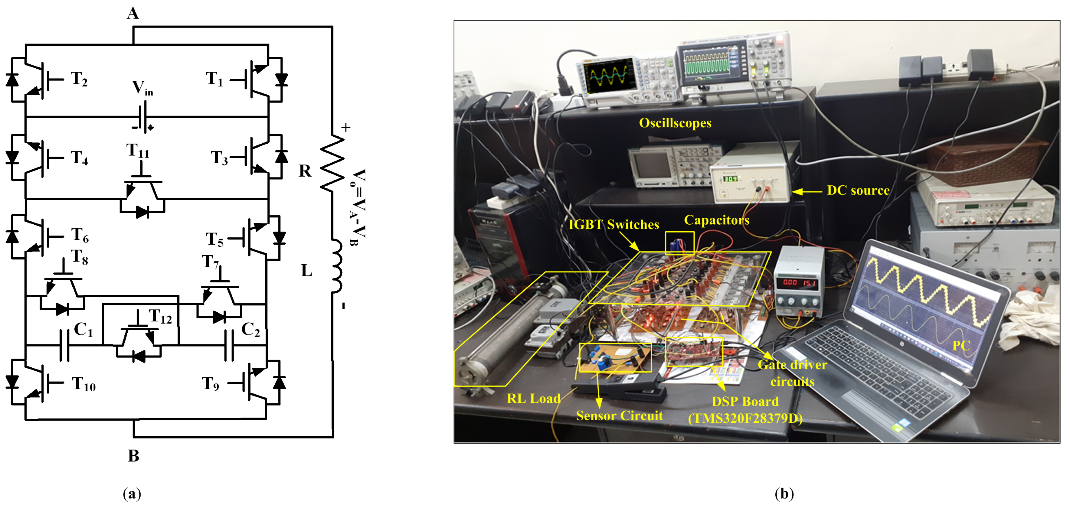
2.1. Operation of DB9LI

The operating states of the investigated inverter are demonstrated in Table 2. The output voltage is maintained at ± V i n state when the switches T 3 and T 4 on during 0 and capacitors C 1 and C 2 are charged up to V i n /2. Furthermore, the capacitors are associated parallel during ± V i n /2 and ± 3 V i n /2 states. Hence, the voltage across the capacitors are balanced. During discharging states ± V i n /2 and ±2 V i n , capacitors are discharged through the load. The investigated topology does not require external voltage balancing circuit.

2.2. Assessment of DB9LI

Table 3 compares the DB9LI topology with other recent competitive 9-level topologies in terms of the number of various components involved and number of levels generated. The reduction in components count makes the circuit control easy and compact. The DB9LI employs lower PIV switches which contributes to a low per unit total standing voltage (TSVpu) of the circuit. Compared to the topologies in References [38,39,40,41], the investigated topology has lower per unit TSV. Also, unlike some other compared topologies DB9LI has the inherent capacitor voltage balancing capability. There are other disadvantages that are linked with some other topologies. For example, In the switched capacitor modules (SCM) in References [38,39], switches employed in the second stage of H-Bridge have to withstand the voltages equal to twice of the input DC source voltage and series combination of switches are required so that the PIV of all switches does not exceed the input voltage. Compact Switched Capacitor Multilevel Inverter (CSCMLI) in Reference [42] minimize the blocking voltage across the switches and the high switch count of SCM [39]. In the topology in Reference [40], the number of capacitors required for the nine level generation are three and with different ratings, while in the investigated topology two capacitors having same ratings are required.

3. Metaheuristic-Based Modulation of DB9LI

Depending on the application, it is sometimes required to have a constant output voltage. For such operations it is required that the switching occurs at instances that produce an output voltage with minimum harmonic content. Selective Harmonic Elimination (SHE) is one such technique [29]. In order to produce the optimum angles in these constrained environments optimization techniques are employed. Conventional techniques are based on solving the transcendental equations by using techniques such as Newton-Raphson method [30]. Nowadays, nature inspired techniques like genetic algorithm [31], particle swarm optimization [32], differential evolution [33] are being employed. In this work a DE-based technique is employed. DE is a search based algorithm that offers the advantages of a guaranteed convergence and simplicity. In comparison with other optimization techniques such as GA, DE offers a faster selection process and fewer control parameters, as discussed in detail in Reference [44].

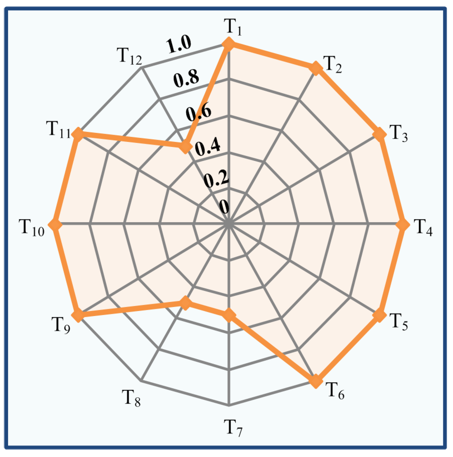
3.1. Selective Harmonic Elimination and Mitigation

SHE and SHM are widely discussed in the literature where the energy of lower order harmonics is controlled by maneuvering with the transition instances of the output voltages. The multilevel waveforms must exhibit half-wave and quarter-wave symmetry. And thus it is required to evaluate angles that are under the quarter wave area. Therefore, for a nine-level operation four optimum angles must be deduced. The discussion on transcendental equations is as follows.
The output of a 9-level inverter in terms of Fourier expansion is represented as:
V o = a o + n = 1 , 2 a n cos ω t + b n sin ω t .
Due to symmetry, the DC component a o and the even harmonics are neglected. The even harmonic coefficient is represented as:
b n = 2 T o T o V o ( t ) sin n ω o t d t n = 1 , 3 , 5 , .
This can be further solved into:
b n = 4 E n π i = 1 4 cos n θ i .
Now, the objective functions for the SHE and SHM will be defined according to the following conditions and constraints. For SHE:
m = 3 , 5 , 7 n = 1 , 2 , 4 cos m θ n = 0 .
And for SHM:
m = 3 , 5 , 49 n = 1 , 2 , 4 cos m θ n = min ,
where m is the harmonic number and n defines the angle number. The constraint on angles is as follows:
0 < θ 1 < θ 2 < θ 3 < θ 4 < 90 .

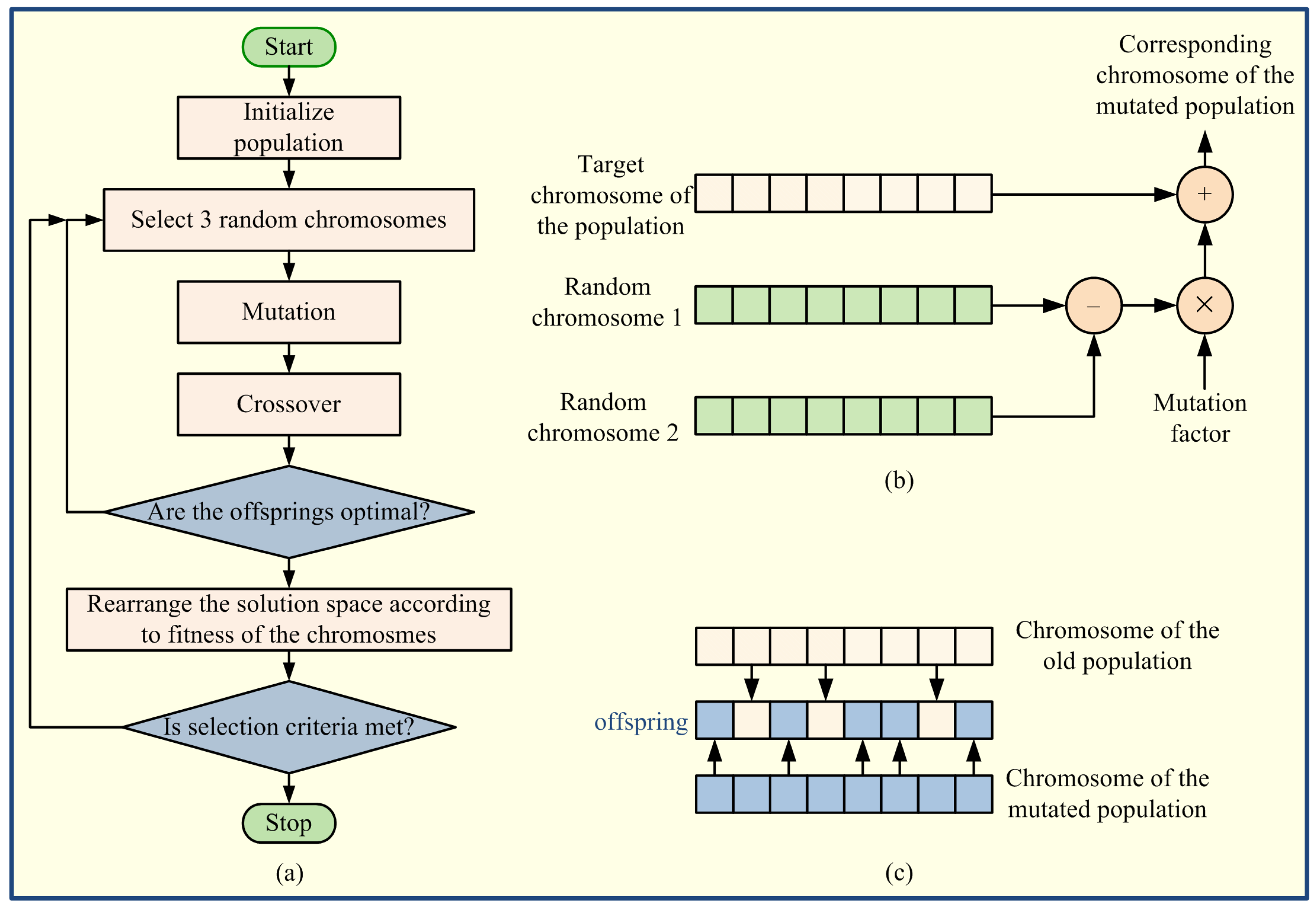
3.2. Differential Evolution

DE is an efficient and simple metaheuristic optimization tool that is utilized to solve the minimization problems that are difficult to solve with conventional optimization tools such as Newton-Raphson method [45]. DE imitates the natural process of evolution and the survival of the fittest. The process is briefly described in Figure 3a. A chromosome consists of all the variables. For example, the problem here is to find four angles; so, these angles will form a chromosome of 32 bits (8 bit for each variable). A random initial population of such chromosomes is developed in the software environment and rearranged according to its fitness towards the objective function. An objective function is a function that is developed as a minimization problem for the situation under consideration. For the analysis here, the objective function will differ according to (4) and (5) depending on the SHE or SHM operation.
Next, the mutation is performed on the data as shown for one variable of the chromosome in Figure 3b where three chromosomes including the target chromosome is chosen. The choice of the chromosomes other than the target chromosome is purely random and is decided by the software. The data is mutated by a factor which can be chosen in the range of 0 to 2. Thus a new chromosome corresponding to the target chromosome is generated and stored for a while. The a new chromosome is developed by randomly selecting some bits from the old chromosome and the new mutated chromosome to form a new chromosome. This step is known as crossover, and the chromosome is the final child or offspring of the target chromosomes. Now, if the fitness of the chromosome is better than the previous chromosome, it takes its place, otherwise it is discarded. The process repeats until a predefined number of iterations are reached. The parameters of DE are shown in Table 4.
The DE algorithm based on the above discussion and Figure 3a was developed in MATLAB/Simulink. The optimal angles were obtained as the final solutions of optimization problem. Using these angles, the simulation and experimental results of SHE and SHM were produced and are presented in Figure 4. Figure 4a exhibit the simulation and experimental results of SHE, where the complete elimination of the 5th and 7th harmonic is visible. On the other hand the results of SHM (Figure 4b) exhibits the mitigation of overall harmonics, and thus total harmonic distortion (THD) is lower than the waveform of SHE.

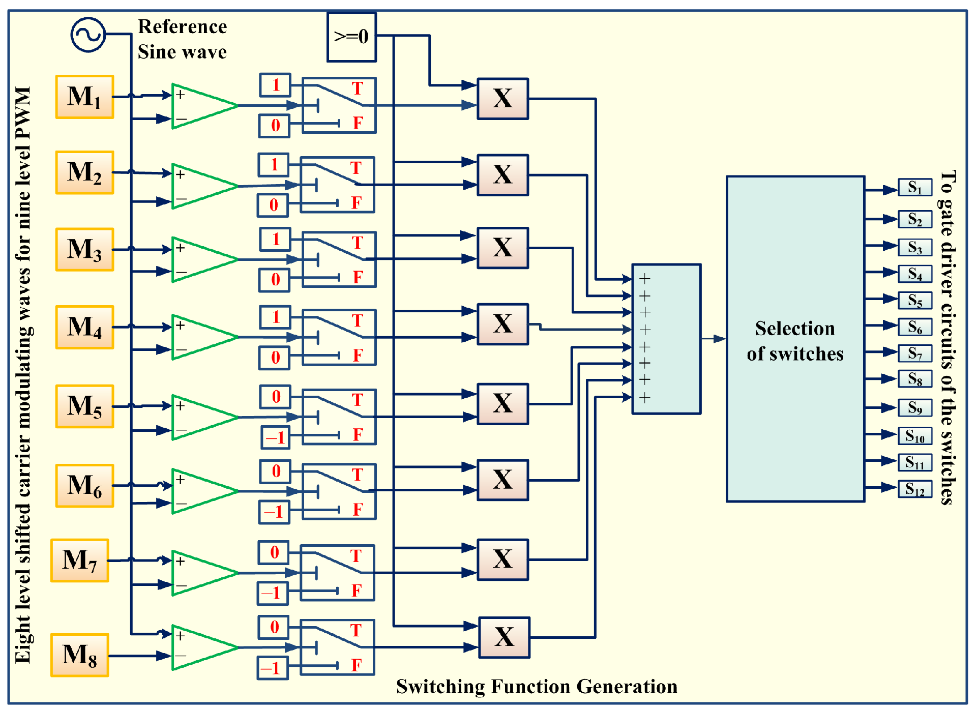
4. Pulse-Width Modulation of DB9LI

Level shifted carrier waveforms that form the half sine waves and quarter sine waves have been obtained, as they exhibit superior performance in mitigation of voltage profile harmonics under the conditions of low-frequency operation. By using (7), the level-shifted quarter sine wave and half-sine carrier waves can be generated:
m 3 × | m 1 Π f 1 | m 2 sin ( 2 π f 2 t ) | | ,
where, m 1 , m 2 , m 3 are arbitrary constants; f 1 and f 1 are the frequencies of the square wave function Π and the sinusoidal function.
It is the ratio of the frequencies of square function and sinusoidal function( f 1 : f 2 ) which decides the shape of the final carrier waveform. By varying this ratio, the nature of the obtained carrier can be modified. For example, the condition f 1 = f 2 results in a half- Sine waveform. The value of the factors m 1 , m 2 , and m 3 are selected as 0.5, 0.5, and 0.5 respectively for the generation of half-sine carrier wave, and the value of frequencies f 1 and f 2 are taken as 7000 Hz. Similarly, (7) is utilized to generate a quarter-sine wave by taking the condition f 1 = 2 f 2 . With f 1 = 7000 Hz and f 2 = 3500 Hz and the value of factors m 1 , m 2 and m 3 are being taken as 0.5, 0.5, and 0.5, respectively. By shifting the obtained halfsine carrier waves or the quarter-sine carrier waves by a fixed magnitude in the positive and negative directions, eight carrier signals of switching frequency are generated for nine-level shifted-PWM that can be identified as M 8 , M 7 , M 6 , M 5 , M 4 , M 3 , M 2 and M 1 in Figure 5. By the comparison of V r e f and the carrier waves, the pulses for corresponding voltage levels are generated. The generation of zero level is achieved when the reference voltage is between M 5 and M 4 . Along with these waveforms, the conventional levelshifted carrier and a sinusoidal carrier is also taken. The comparative assessment of each modulation technique is discussed further in this paper.

4.1. Control Strategy

Multicarrier PWM control is used for controlling each IGBT switch used in this topology as shown in Figure 5. The carriers are level disposed vertically and each of same amplitude, frequency and phase. The switching strategy being used is implemented in such a manner that T 11 is fired when V r e f > M 1 or M 2 < V r e f < M 1 or M 8 < V r e f < M 7 or V r e f < M 8 or in other words, T 11 is fired when T 1 and T 4 are on and T 3 is off (or T 2 and T 3 is on and T 4 is off), as exhibited in Figure 5. Likewise, T 12 is fired when V r e f > M 1 or M 3 < V r e f < M 2 or M 5 < V r e f < M 4 or M 7 < V r e f < M 6 or V r e f < M 8 . Another way is that T 12 should be fired when T 7 and T 8 are off. By using this technique control circuitry is designed. These carriers are compared with the sinusoidal reference wave of power frequency and of a unit magnitude.
After comparing with the reference signal, the generated output is a pulse signal of unit magnitude. In the next stage, these signals are separated to distinguish the positive half cycle and a negative half cycle of output voltage nine-level wave. For this, the logic is applied by using a two-way switch, which gives output according to the threshold value. The four signals that pertain to positive half cycle are checked whether the signal is greater than 0 or not, and depending upon the previously obtained signal, the output of this stage for the positive half cycle is a pulse of magnitude 0 to 1 and for negative half-cycle pulses of magnitude 0 to −1.
In the later stage these pulses are tested for shifting the pulses to different states −4, −3, −2, −1, 0, +1, +2, +3, +4 levels. After getting output from this point, all pulses are added to generate a nine-level output waveform that is, switching function is constructed as depicted in Figure 5, which is going to be followed by output voltage waveform. MATLAB functional block is used to create logic to fire the switches according to the switching state table.

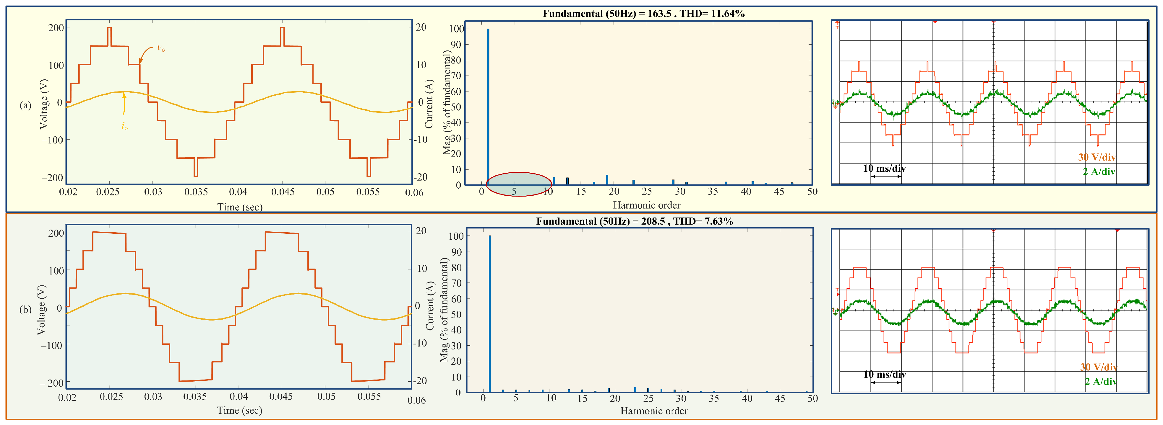
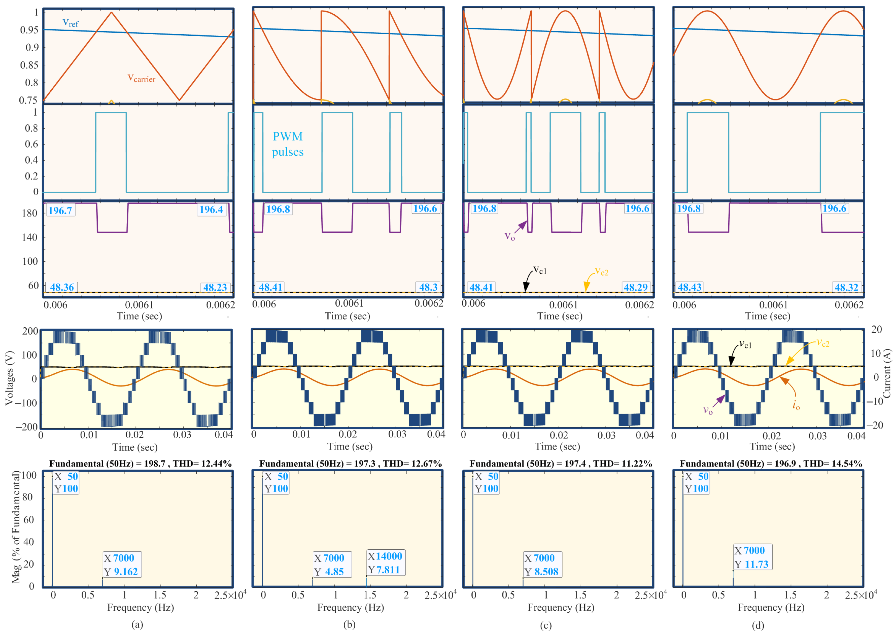
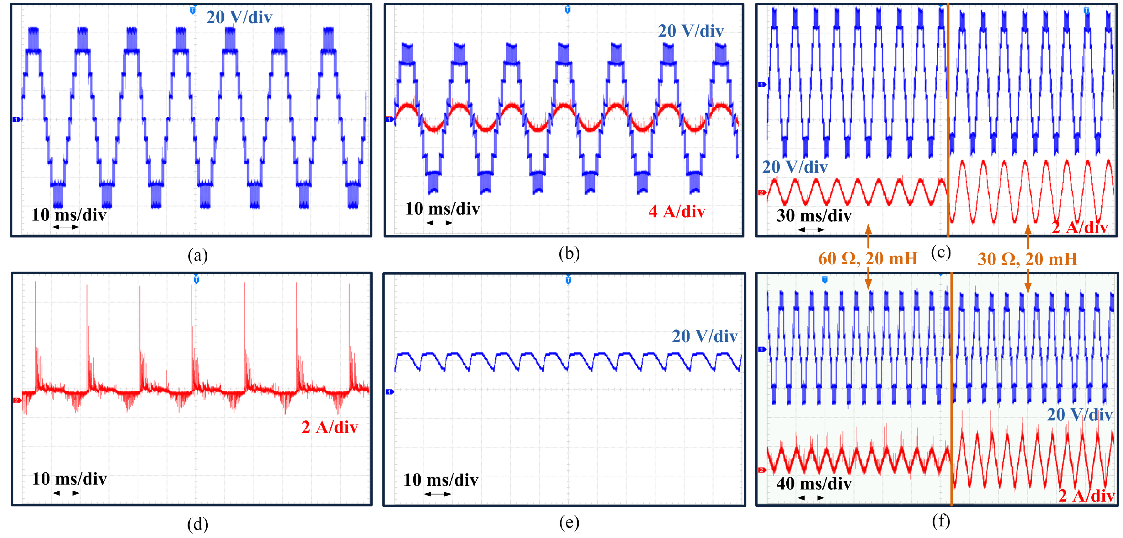
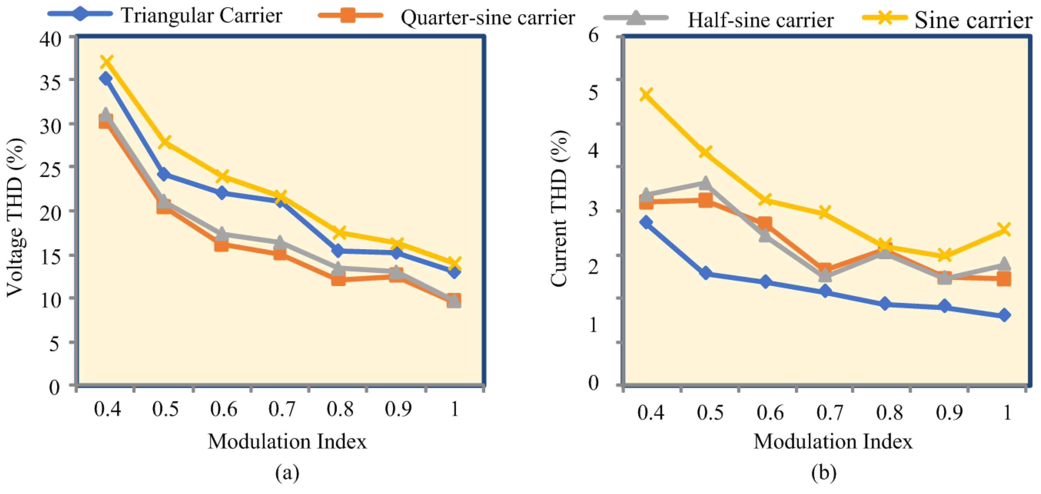
4.2. Results and Discussion

Simulations of DB9LI is performed to analyze the effect of different type of carrier waves on total harmonic distortion (THD) in load voltage and currents. The comparative analysis is done to check the suitability of a particular type of carrier according to the required application. In Figure 6a–d, pulse generation employing all four types of carrier waves discussed in previous subsection is shown. In addition, load voltage and current are also exhibited for each condition in the figure with voltage THD profiles. Simulation has been carried out in the MATLAB/Simulink environment. Parameters taken for the simulation purpose are given in Table 1. The input DC source voltage is taken as 100 V for all modulation techniques. Constant AC Load of resistance 20 Ω and inductor of 20 mH is applied and two capacitors C 1 and C 2 of 4700 μ F have been used. The AC load voltage has nine-level boosted output and its harmonic content reside on the multiples of 7000 Hz, that is switching frequency as shown in Figure 6. From Figure 6, it is also seen that the load voltage THD percentage is maximum in case of sine-sine PWM that is, 14.54% and minimum in the case of half-sine PWM that is, 11.22%. Furthermore, the output fundamental voltage is nearly around to 197.5 V which has a frequency of 50 Hz. Lastly, the load current is sinusoidal and the capacitor voltage is maintained at 50 V and contains 4% ripple.
In Figure 7, the experimental results of load voltage, load current, capacitor voltage and capacitor current under various conditions are exhibited by application the triangular level-shifted PWM technique on the DB9LI. In the whole experimental analysis, the 30 V DC source voltage is being used. In Figure 7a, the nine levels no-load voltage is demonstrated when the modulation index m a = 1. Figure 7a clearly shows that the voltage at output terminals is 60 V which supports the statement that the DB9LI is capable of boosting voltage to twice of applied DC voltage. In Figure 7b, the output voltage and current waveform are being shown under the loaded condition, when the load resistance is R = 30 Ω and L = 20 mH. In Figure 7c, the voltage and current waveforms are being presented under the variable load condition in which load impedance is being varied from R = 60 Ω & L = 20 mH to R = 30 Ω & 20 mH and exhibits the robust nature of DB9LI, as with the variation in load, output voltage magnitude, the number of levels and the waveshape remains almost unaffected. Figure 7d shows the capacitor current waveform under the same condition as in Figure 7b (i.e., when Z = 30 Ω + 20 mH). The current and voltage of one capacitor is shown during the charging and discharging periods in Figure 7d,e. In Figure 7f, the output voltage waveform under the variable load condition is being shown, when the load impedance is being varied from R = 60 Ω & L = 20 mH to R = 30 Ω & L = 20 mH when the amplitude modulation index is being taken as m a = 0.7.
Figure 8a presents the variation in output THD percentage of Voltage with the variation in modulation index when triangular, half-sine and quarter-sine and sine waves are being used as carrier waves by varying the modulation index from 0.4 to 1.0 at the same frequency as mentioned in the control strategy of DB9LI. The inverter circuit is connected to R-L load having values of 30 Ω and 20 mH for the three cases. Figure 8a also gives a clear insight into the benefit of using quarter-sine wave from the voltage THD perspective over the half-sine, triangular carrier or sine carrier, and shows that the THD percentage is low in it. From Figure 8a, it can also be observed that the variation of THD with modulation index is more in case of the sine carrier as compared to the triangle, quarter and half-sine wave PWM. Figure 8b shows the variation of percentage THD in current with the variation in modulation index corresponding to half-sine wave, quarter-sine, sine and triangular carriers, when the amplitude modulation index is being varied from 0.4 to 1. From these two figures (Figure 8a,b), it can be observed that with increase in the modulation index, both the percentage voltage and current THD are following a drooping pattern.

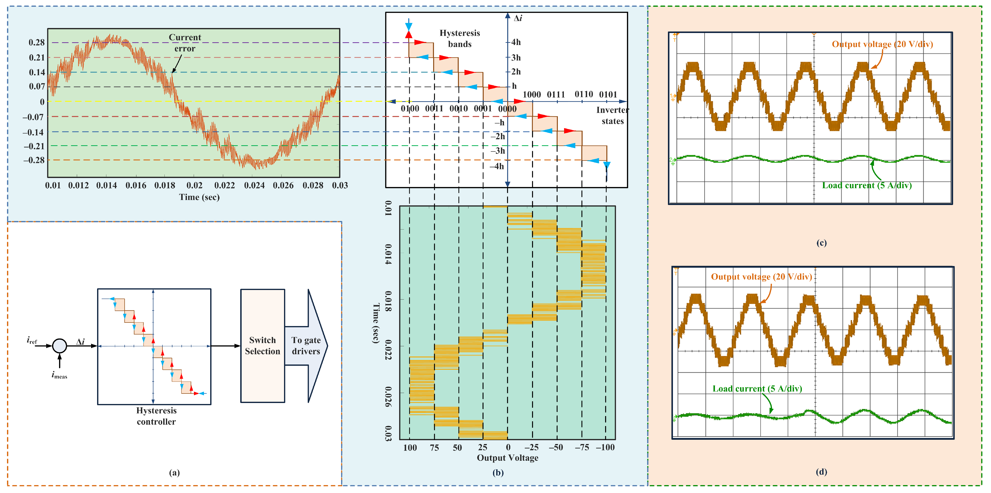
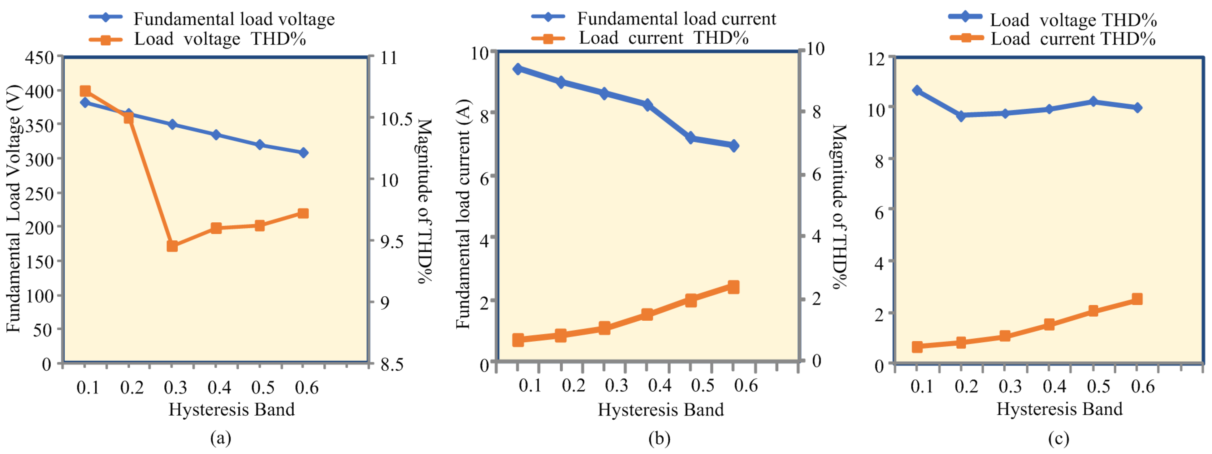
5. Hysteresis Control of DB9LI

Hysteresis current control technique is a control technique widely applied for converters and drives. There are various advantages of this technique like a good dynamic response, unconditional stability and wide bandwidth of command. However, this control is sensitive to noise as slight disturbance in the error will lead an undesired voltage level, which can lead to undesirable consequences, especially in applications like electric vehicles. Hysteresis is closed-loop control in which continuously load current is monitored. In DB9LI there is inheriting capacitors voltage balancing. But if in case balancing is required, then by proper PI control, it can be achieved. The load current error is compared with hysteresis bands to generate the firing signals for the inverter. This technique has been applied to two-level converter control and has shown its robustness and simplicity. Hysteresis in multilevel inverters is also becoming popular because of its undeniable advantages over other technologies.
The objective of multilevel current control is to trigger the switching signal by keeping the load current follow the reference under the specified hysteresis band. The multi-band hysteresis control technique uses symmetrical hysteresis bands called as upper and lower bands to control the firing of switches to the adjacent level. when the error current signal passes the inner border at level one and the output is increased or decreased by one level if the limit is crossed. The advancement in the voltage would cause the current error ( Δ i ) to change the direction opposite to the previous to keep it in band limit. The error may reach to the next boundary if the error has not changed the direction. When the next boundary level reaches the inverter would switch the next voltage level. This path is followed until the error current reverses its direction. The voltage applied at the positive and negative ends should be able to force the current to come back to the required limit. As it is seen in Figure 9, actual rated current (i) is sinusoidal, rated, reference current ( i r e f ) and the difference between load current and reference current is ( Δ i ) or current error. Eight bands (0 h), (−h →−2 h), (−2 h →−3 h), (−3 h 4 h), (0 → h), (h → 2 h), (2 h → 3 h) and (3 h → 4 h) of bandwidth about 2% to 5% rated load current is taken. For achieving nine-level voltage generation at the output, It is the necessary condition to maintain the capacitor voltage set point equal to V i n / 2 . Thus, the nine-level voltages are therefore obtained as given in Table 2. Figure 9 depicts that the current error ( Δ i ), is quantified into eight equal bands which results into the ten zones in the abscissa axis. The vertical axis is quantified into nine distinct values corresponding to the nine voltage levels at the output. The subsequent variation in the transition condition depends on the behavior of the current error. For instance, if the initial state is V 1 / 2 , the further reduction of the current error Δ i , below the value h causes a transition to state zero (0). Contrary to that, if the current error Δ i ,increases above the h value, then, an instantaneous transition to the state V 1 takes place. When the actual load current is lower than its reference, then the application of a positive voltage across the load results in rapprochement. Thus, the positive voltages are applied when the current error Δ i , which is the difference between actual load current and its reference, is negative. In contrast to that, the negative voltages are applied when the current error is positive. The nine states and their transition conditions are depicted in Figure 9.
In the Figure 10 the graphs shows the total harmonic distortion (THD) for the output voltage and current waveform. The variation of fundamental load current as well as the variation in percentage THD for different values of hysteresis band (h) is shown in Figure 10a. It can be observed that as the hysteresis bandwidth increases, magnitude of the fundamental load current decreases. Also, with the increase in the hysteresis band, the percentage THD in the load current increases in approximate proportion.The anomalous behavior of the load voltage THD variation with change in hysteresis band is being shown in the Figure 10b where, with the increase in hysteresis bandwidth, the load voltage THD first decreases, reaches a minimum value, experiences a slight increment and then with further increase in h decreases sharply. On the other hand, the value of fundamental load voltage exhibits a simple linearly decreasing pattern with the increase in hysteresis bandwidth. It can be readily observed that within the range of h from 0 to 0.6, the minimum percentage THD occurs when h is 0.2. So, from the % THD consideration, the best operating point is corresponding to h = 0.6.To understand the behavior of current and voltage THD for the wide range of hysteresis band. In the Figure 10c. clear insight is given to the variation of these parameters. In the fixed hysteresis band control switching frequency varies as the hysteresis band changes also the switching frequencies of all the switches is also different and varies with the bandwidth. The variation of THD percentage with voltage and current is taken by keeping the load value of 20 Ω & 20 mH. As we can see in the graph, the voltage THD% is maximum when the bandwidth is small that is 0.1 and minimum at h = 0.2 also it can be seen that the change in THD % is not much varying but the current THD % values are changing with little bit more slope. It has been changed from 0.5% at h = 0.1 to 2.23% at h = 0.6.

6. Conclusions

In this paper, a dual boost nine-level inverter (DB9LI) has been analyzed and implemented using different modulation strategies and hysteresis eight-band current control. For the modulation, low switching frequency (SHE and SHM) and high switching frequency (PWM) schemes were implemented. The DE based metaheuristic approach was employed to determine the angles of switching between the voltage levels for the SHE and SHM techniques. The angles produced were found to reduce the selected lower order harmonics and significantly reduce the overall harmonics. Further, the analysis and implementation of PWM techniques on the basis of different carrier waves was performed using triangular, quarter-sine, half-sine and sine carriers, and it was concluded that from the voltage THD point of view, the half-sine carrier exhibited superior performance and the sine carrier wave was found to be the least fit candidate. Lastly, the eight-band hysteresis control was applied on DB9LI, and through analysis it was concluded that the percentage voltage THD was found to be minimum when the hysteresis bandwidth (h) was equal to 0.3. The analysis and verification of these techniques on DB9LI was done in MATLAB/Simulink environment and validated on an experimental prototype.

Author Contributions

Conceptualization, D.U., S.A.K., M.A. and M.T.; Writing—original draft, D.U. and S.A.K.; Writing—review & editing, M.A., M.T., A.S., R.K.C. and M.J.R. All authors contributed collectively to the manuscript preparation. All authors have read and agreed to the published version of the manuscript.

Funding

This publication was made possible by the Collaborative Research Grant Scheme (CRGS) project sponsored by Capability Systems Centre, University of New South Wales-Canberra, Australia to the Department of Electrical Engineering, Aligarh Muslim University, India having project grant no: [CRGS/Mohd Tariq/02].

Acknowledgments

The authors also acknowledge the support provided by the Hardware-In-the-Loop (HIL) Lab, Department of Electrical Engineering, Aligarh Muslim University, India.

Conflicts of Interest

The authors declare no conflict of interest.

References

  1. Norambuena, M.; Kouro, S.; Dieckerhoff, S.; Rodríguez, J. Reduced Multilevel Converter: A Novel Multilevel Converter with Reduced Number of Active Switches. IEEE Trans. Ind. Electron. 2017, 65, 3636–3645. [Google Scholar] [CrossRef]
  2. Vahedi, H.; Shojaei, A.A.; Dessaint, L.A.; Al-Haddad, K. Reduced DC-Link Voltage Active Power Filter Using Modified PUC5 Converter. IEEE Trans. Power Electron. 2018, 33, 943–947. [Google Scholar] [CrossRef]
  3. Gontijo, G.; Wang, S.; Kerekes, T.; Teodorescu, R. New ac-ac modular multilevel converter solution for medium-voltage machine-drive applications: Modular multilevel series converter. Energies 2020, 13, 3664. [Google Scholar] [CrossRef]
  4. Rodriguez, J.; Bernet, S.; Steimer, P.K.; Lizama, I.E. A survey on neutral-point-clamped inverters. IEEE Trans. Ind. Electron. 2010, 57, 2219–2230. [Google Scholar] [CrossRef]
  5. Tackie, S.N.; Babaei, E. Modified topology for three-phase multilevel inverters based on a developed H-bridge inverter. Electronics 2020, 9, 1848. [Google Scholar] [CrossRef]
  6. Laali, S.; Babaei, E. Optimum Structures of Proposed New Cascaded Multilevel Inverter with Reduced Number of Components. IEEE Trans. Ind. Electron. 2015, 62, 6887–6895. [Google Scholar] [CrossRef]
  7. Malinowski, M.; Gopakumar, K.; Rodriguez, J.; Perez, M.A. A survey on cascaded multilevel inverters. IEEE Trans. Ind. Electron. 2010, 57, 2197–2206. [Google Scholar] [CrossRef]
  8. Lai, Y.; Shyu, F. New topology for hybrid multilevel inverter. In Proceedings of the 2002 International Conference on Power Electronics, Machines and Drives (Conf. Publ. No. 487), Sante Fe, NM, USA, 4–7 June 2002; pp. 1–6. [Google Scholar]
  9. Thamizharasan, S.; Baskaran, J.; Ramkumar, S.; Jeevananthan, S. Electrical Power and Energy Systems A new dual bridge multilevel dc-link inverter topology. Electr. Power Energy Syst. 2013, 45, 376–383. [Google Scholar] [CrossRef]
  10. Rech, C.; Pinheiro, J.R. Hybrid Multilevel Converters: Unified Analysis and Design Considerations. IEEE Trans. Ind. Electron. 2007, 54, 1092–1104. [Google Scholar] [CrossRef]
  11. Azimi, E.; Khodaparast, A.; Rostami, M.J.; Adabi, J.; Adabi, M.E.; Rezanejad, M.; Rodrigues, E.M.G.; Pouresmaeil, E. X-Type Step-Up Multi-Level Inverter with Reduced Component Count Based on Switched-Capacitor Concept. Electronics 2020, 9, 1987. [Google Scholar] [CrossRef]
  12. Ramkumar, S.; Kamaraj, V.; Thamizharasan, S.; Jeevananthan, S. A new series parallel switched multilevel dc-link inverter topology. Electr. Power Energy Syst. 2012, 36, 93–99. [Google Scholar] [CrossRef]
  13. Sato, Y.; Member, S.; Uno, M.; Nagata, H. Nonisolated Multiport Converters Based on Integration of PWM Converter and Phase-Shift Switched Capacitor Converter. IEEE Trans. Power Electron. 2020, 35, 455–470. [Google Scholar] [CrossRef]
  14. Gupta, K.K.; Ranjan, A.; Bhatnagar, P.; Sahu, L.K.; Jain, S. Multilevel Inverter Topologies With Reduced Device Count: A Review. IEEE Trans. Power Electron. 2016, 31, 135–151. [Google Scholar] [CrossRef]
  15. Zhang, C.; Gao, Z. A Novel Multilevel DC/AC Inverter Based on Three-Level Half Bridge with Voltage Vector Selecting Algorithm. IEEE Access 2019, 7, 88733–88742. [Google Scholar] [CrossRef]
  16. Dhanamjayulu, C.; Meikandasivam, S. Implementation and Comparison of Symmetric and Asymmetric Multilevel Inverters for Dynamic Loads. IEEE Access 2017, 6, 738–746. [Google Scholar] [CrossRef]
  17. Karthikeyan, D.; Vijayakumar, K.; Jagabar Sathik, M. Generalized cascaded symmetric and level doubling multilevel converter topology with reduced THD for photovoltaic applications. Electronics 2019, 8, 161. [Google Scholar] [CrossRef] [Green Version]
  18. Kang, J.W.; Hyun, S.W.; Ha, J.O.; Won, C.Y. Improved neutral-point voltage-shifting strategy for power balancing in cascaded NPC/H-bridge inverter. Electronics 2018, 7, 167. [Google Scholar] [CrossRef] [Green Version]
  19. Taghvaie, A.; Adabi, J.; Rezanejad, M. A Self-Balanced Step-Up Multilevel Inverter Based on Switched-Capacitor Structure. IEEE Trans. Power Electron. 2018, 33, 199–209. [Google Scholar] [CrossRef]
  20. Taghvaie, A.; Adabi, J.; Rezanejad, M. A Multilevel Inverter Structure based on Combination of Switched-Capacitors and DC Sources. IEEE Trans. Ind. Inform. 2017, 13, 2162–2171. [Google Scholar] [CrossRef]
  21. Vahedi, H.; Sharifzadeh, M.; Al-Haddad, K. Modified Seven-Level Pack U-Cell Inverter for Photovoltaic Applications. IEEE J. Emerg. Sel. Top. Power Electron. 2018, 6, 1508–1516. [Google Scholar] [CrossRef]
  22. Iqbal, A.; Meraj, M.; Tariq, M.; Lodi, K.A.; Maswood, A.I. Experimental Investigation and Comparative Evaluation of Standard Level Shifted Multi- Carrier Modulation Schemes with a Constraint GA Based SHE Techniques for Seven-Level. IEEE Access 2019, 7, 100605–100617. [Google Scholar] [CrossRef]
  23. Shojaei, A.A.; Najafi, B.; Vahedi, H. Standalone operation of modified seven-level packed U-Cell (MPUC) single-phase inverter. Electronics 2019, 8, 268. [Google Scholar] [CrossRef] [Green Version]
  24. Ounejjar, Y.; Al-Haddad, K.; Dessaint, L.A. A Novel Six-Band Hysteresis Control for the Packed U Cells Seven-Level Converter: Experimental Validation. IEEE Trans. Ind. Electron. 2012, 59, 3808–3816. [Google Scholar] [CrossRef]
  25. Shuvo, S.; Hossain, E.; Islam, T.; Akib, A.; Padmanaban, S.; Khan, M.Z.R. Design and Hardware Implementation Considerations of Modified Multilevel Cascaded H-Bridge Inverter for Photovoltaic System. IEEE Access 2019, 7, 16504–16524. [Google Scholar] [CrossRef]
  26. Sharifzadeh, M.; Al-Haddad, K. Packed E-Cell (PEC) Converter Topology Operation and Experimental Validation. IEEE Access 2019, 7, 93049–93061. [Google Scholar] [CrossRef]
  27. Sebaaly, F.; Sharifzadeh, M.; Kanaan, H.Y.; Al-haddad, K. Multilevel Switching Mode Operation of Finite Set Model Predictive Control for Grid-Connected Packed E-Cell (PEC) Inverter. IEEE Trans. Ind. Electron. 2020. [Google Scholar] [CrossRef]
  28. Babaei, E.; Kangarlu, M.F.; Mazgar, F.N. Symmetric and asymmetric multilevel inverter topologies with reduced switching devices. Electr. Power Syst. Res. 2012, 86, 122–130. [Google Scholar] [CrossRef]
  29. Sharifzadeh, M.; Vahedi, H.; Al-Haddad, K. New Constraint in SHE-PWM for Single-Phase Inverter Applications. IEEE Trans. Ind. Appl. 2018, 54, 4554–4562. [Google Scholar] [CrossRef]
  30. Al-Hitmi, M.; Ahmad, S.; Iqbal, A.; Padmanaban, S.; Ashraf, I. Selective Harmonic Elimination in a Wide Modulation Range using Modified Newton-Raphson and Pattern Generation Methods for a Multilevel Inverter. Energies 2018, 11, 458. [Google Scholar] [CrossRef] [Green Version]
  31. Lodi, K.A.; Azeem, A.; Tariq, M.; Ali, M.; Bharatiraja, C. Harmonic Minimization in Modified PUC-5 Inverter Using Genetic Algorithm. In Proceedings of the 2018 IEEE International Conference on Power Electronics, Drives and Energy Systems (PEDES), Chennai, India, 18–21 December 2018; pp. 1–6. [Google Scholar] [CrossRef]
  32. Luo, L.; Abdulkareem, S.S.; Rezvani, A.; Miveh, M.R.; Samad, S.; Aljojo, N.; Pazhoohesh, M. Optimal scheduling of a renewable based microgrid considering photovoltaic system and battery energy storage under uncertainty. J. Energy Storage 2020, 28, 101306. [Google Scholar] [CrossRef]
  33. Ali, M.; Iqbal, A.; Anees, M.A.; Khan, M.R.; Rahman, K.; Ayyub, M. Differential evolution-based pulse-width modulation technique for multiphase MC. IET Power Electron. 2019, 12, 2224–2235. [Google Scholar] [CrossRef]
  34. Shukla, A.; Ghosh, A.; Joshi, A. Hysteresis Modulation of Multilevel Inverters. IEEE Trans. Power Electron. 2011, 26, 1396–1409. [Google Scholar] [CrossRef]
  35. Sarkar, I.; Fernandes, B.G. Multi-carrier Based Hysteresis Current Control Technique For Five-Level Symmetric Cascaded Multilevel Converter. In Proceedings of the 2016 IEEE International Conference on Power Electronics, Drives and Energy Systems (PEDES), Trivandrum, India, 14–17 December 2016; pp. 1–6. [Google Scholar]
  36. Ounejjar, Y.; Al-Haddad, K. Multiband Hysteresis Controller Of The Novel Three Phase Seven-Level PUC-NPC Converter. In Proceedings of the 39th Annual Conference of the IEEE Industrial Electronics Society (IECON 2013), Vienna, Austria, 10–13 November 2013; pp. 6257–6262. [Google Scholar]
  37. Saeedian, M.; Pouresmaeil, E.; Samadaei, E.; Rodrigues, E.M.G.; Godina, R.; Marzband, M. An Innovative Dual-Boost Nine-Level Inverter with Low-Voltage Rating Switches. Energies 2019, 12, 207. [Google Scholar] [CrossRef] [Green Version]
  38. Siddique, M.D.; Iqbal, A.; Sathik, J.; Mekhilef, S.; Almakhles, D. Design and implementation of a new unity gain nine-level active neutral point clamped multilevel inverter topology. IET Power Electron. 2020, 13, 3204–3208. [Google Scholar] [CrossRef]
  39. Lee, S.S. Single-Stage Switched-Capacitor Module (S3CM) Topology for Cascaded Multilevel Inverter. IEEE Trans. Power Electron. 2018, 33, 8204–8207. [Google Scholar] [CrossRef] [Green Version]
  40. Nakagawa, Y.; Koizumi, H. A Boost-Type Nine-Level Switched Capacitor Inverter. IEEE Trans. Power Electron. 2019, 34, 6522–6532. [Google Scholar] [CrossRef]
  41. Barzegarkhoo, R.; Moradzadeh, M.; Zamiri, E.; Madadi Kojabadi, H.; Blaabjerg, F. A New Boost Switched-Capacitor Multilevel Converter with Reduced Circuit Devices. IEEE Trans. Power Electron. 2018, 33, 6738–6754. [Google Scholar] [CrossRef]
  42. Sathik, M.J.; Krishnasamy, V. Compact Switched Capacitor Multilevel Inverter (CSCMLI) with Self-Voltage Balancing and Boosting Ability. IEEE Trans. Power Electron. 2019, 34, 4009–4013. [Google Scholar] [CrossRef]
  43. Siddique, M.D.; Member, S.; Mekhilef, S.; Member, S.; Mohamed, N. A New Switched Capacitor 7L Inverter with Triple Voltage Gain and Low Voltage Stress. IEEE Trans. Circuits Syst. II Express Briefs 2020, 67, 1294–1298. [Google Scholar] [CrossRef]
  44. Rout, U.K.; Sahu, R.K.; Panda, S. Design and analysis of differential evolution algorithm based automatic generation control for interconnected power system. Ain Shams Eng. J. 2013, 4, 409–421. [Google Scholar] [CrossRef] [Green Version]
  45. Eltaeib, T.; Mahmood, A. Differential evolution: A survey and analysis. Appl. Sci. 2018, 8, 1945. [Google Scholar] [CrossRef] [Green Version]
Figure 1. (a) Circuit schematic and (b) Experimental Setup of of DB9LI.
Electronics 10 00207 g001
Figure 2. Voltage stress across various switches of DB9MLI (with respect to V i n ).
Electronics 10 00207 g002
Figure 3. (a) Flowchart of differential evolution (DE), (b) mutation, and (c) crossover.
Electronics 10 00207 g003
Figure 4. Simulation result, output voltage total harmonic distortion (THD), and experimental result of (a) Selective Harmonic Elimination (SHE) and (b) selective harmonic mitigation (SHM) pulse width modulation (PWM) schemes.
Electronics 10 00207 g004
Figure 5. Generation of switching pulses for sine-PWM schemes.
Electronics 10 00207 g005
Figure 6. Simulation of PWM techniques applied to DB9LI: (a) Sine–Triangle PWM, (b) Sine–Quarter-sine PWM, (c) Sine–Half-sine PWM and (d) Sine–Sine PWM.
Electronics 10 00207 g006
Figure 7. Experimental results of sine–triangle PWM applied to DB9LI: (a) No load voltage, (b) output voltage and load current at 60 Ω , 20 mH, (c) step load change at m a = 1 , (d) capacitor current, (e) capacitor voltage, and (f) step load change at m a = 0.7 .
Electronics 10 00207 g007
Figure 8. Comparison of (a) Voltage THD and (b) Current THD with PWM schemes.
Electronics 10 00207 g008
Figure 9. (a) Schematic of eight-band hysteresis control, (b) concept describing the generation of output voltage levels corresponding to the current error; and experimental results (c) at constant load and (d) with change in load.
Electronics 10 00207 g009
Figure 10. Variation in (a) fundamental voltage and its THD, (b) fundamental current and its THD, and (c) voltage and current THD.
Electronics 10 00207 g010
Table 1. Simulation and experimental parameters of DB9LI.
S. No.ParametersSimulation ValueExperimental ValueQuantity
1.DC Source Voltage100 V30 V1
2.Capacitors4700 μ F4700 μ F, 50 V2
3.Resistive Load30 Ω , 60 Ω 30 Ω , 60 Ω 2
4.Inductive Load20 mH20 mH1
5.Power frequency50 Hz50 Hz-
6.Switching frequency7 kHz7 kHz-
7.ControllerMATLAB/SimulinkTMS320F28379D1
Table 2. Switching States of DB9LI.
SwitchesSwitching Sequence
T 1 111100000
T 2 000011111
T 3 001110111
T 4 111011100
T 5 111110100
T 6 001011111
T 7 010101010
T 8 010101010
T 9 000001111
T 10 111110000
T 11 110000011
T 12 101010111
Levels2 V i n 1.5 V i n V i n 0.5 V i n 0−0.5 V i n V i n −1.5 V i n −2 V i n
Table 3. Comparison of DB9LI with other topologies.
Parameters[43][39][41][42][41]Investigated
Levels799999
Switches121212111012
DC sources111111
Capacitors223222
Boosting324222
TSV p u 5.35.5657.75.25
Table 4. Parameters of DE Algorithm.
S. No.ParameterValue
1.No. of variables4
2.Initial Population50
3.Mutation factor0.5
4.Iterations100
Publisher’s Note: MDPI stays neutral with regard to jurisdictional claims in published maps and institutional affiliations.

