Article

Design of Multi Standard Near Field Communication Outphasing Transmitter with Modulation Wave Shaping

1
STMicroelectronics d.o.o., Tehnološki Park 21, 1000 Ljubljana, Slovenia
2
Faculty of Electrical Engineering, University of Ljubljana, Tržaška Cesta 25, 1000 Ljubljana, Slovenia
*
Author to whom correspondence should be addressed.
Electronics 2021, 10(2), 188; https://doi.org/10.3390/electronics10020188

Submission received: 17 December 2020 / Revised: 7 January 2021 / Accepted: 11 January 2021 / Published: 15 January 2021
(This article belongs to the Special Issue VLSI Circuits & Systems Design)

Abstract

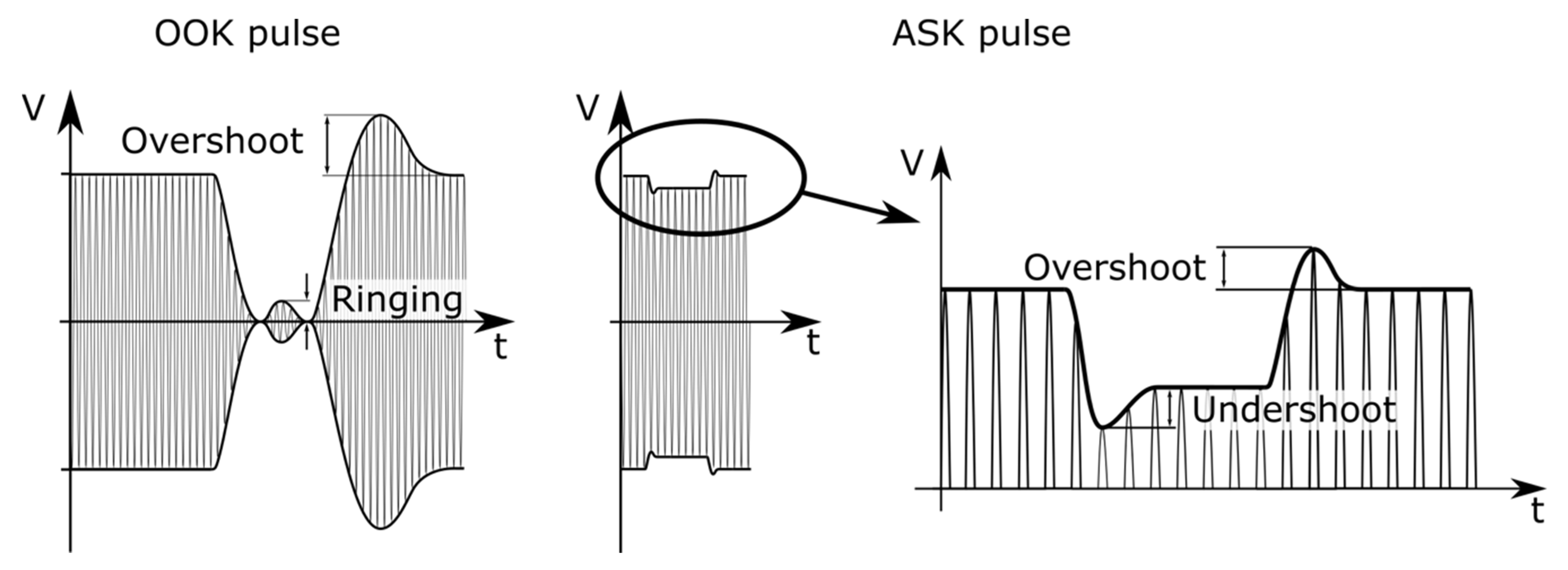
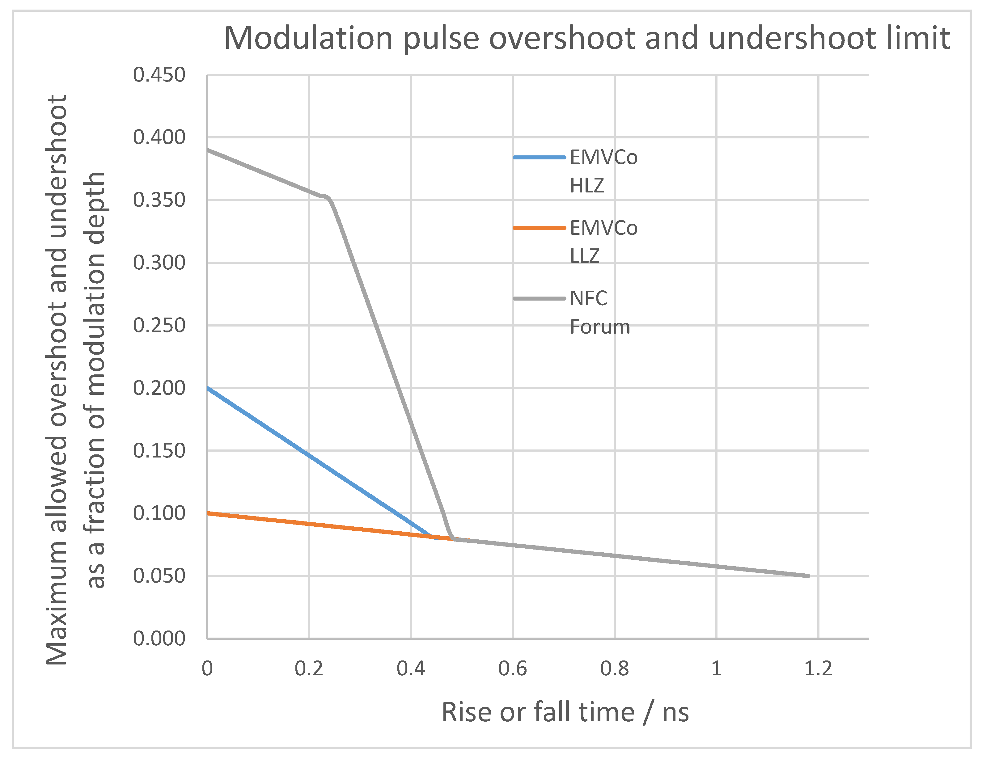
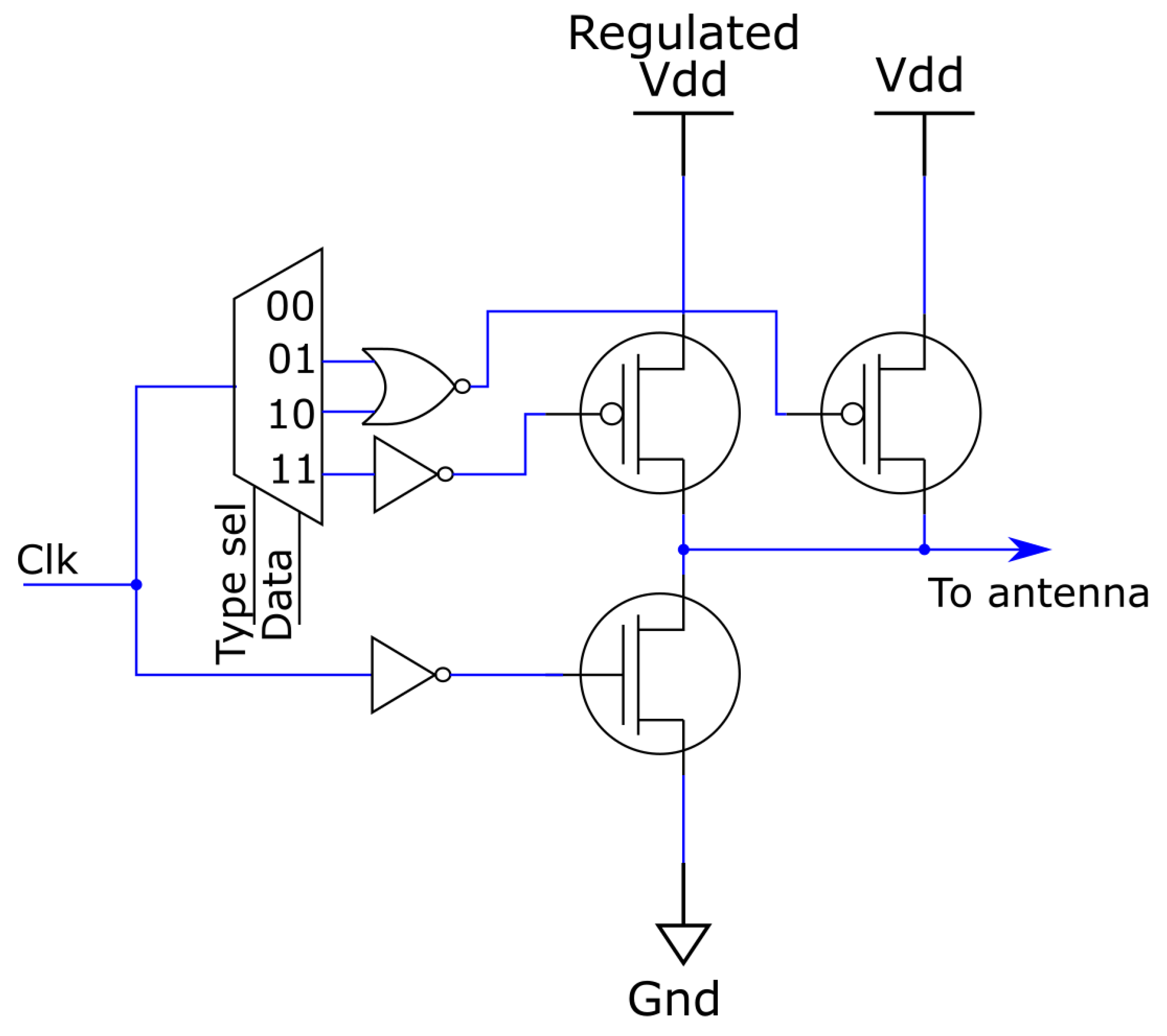
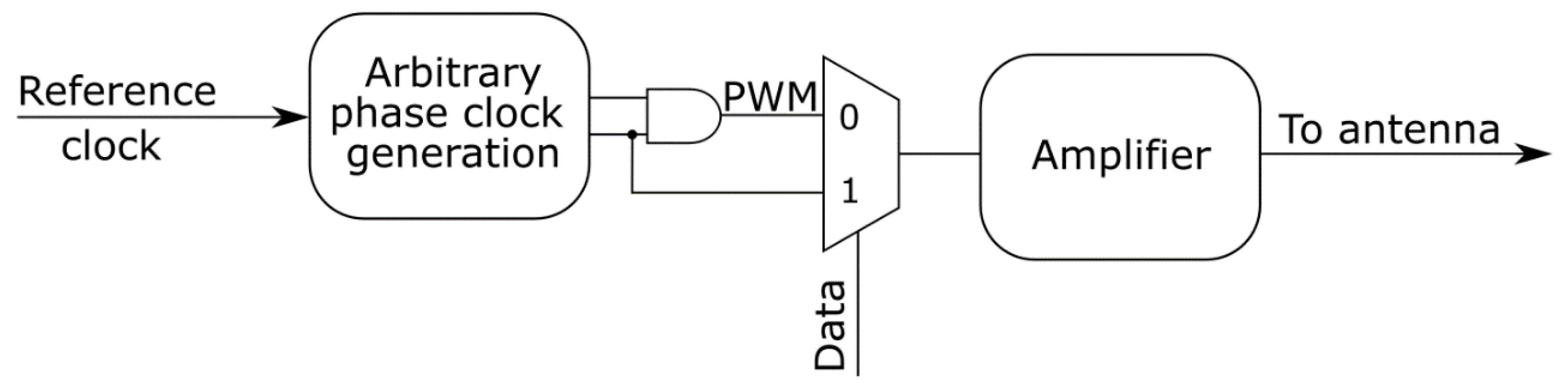
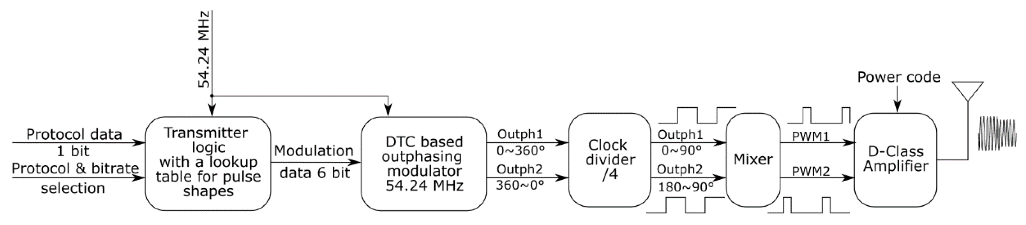
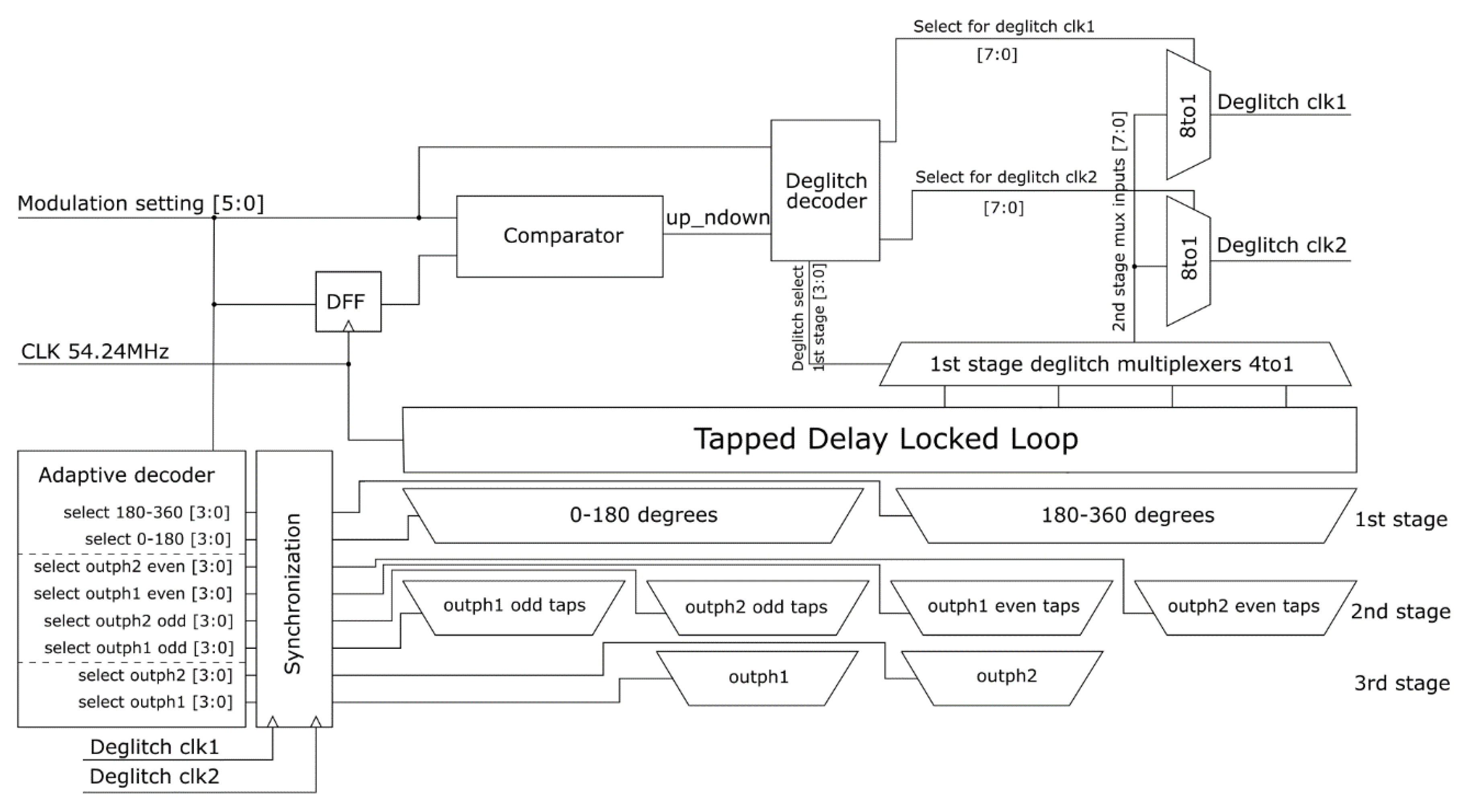
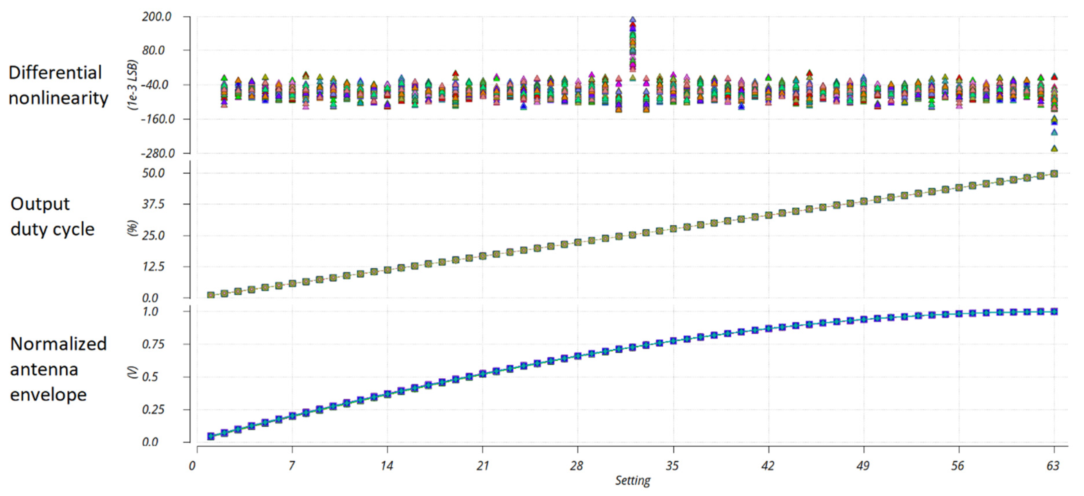
The aim of this work is to tackle the problem of modulation wave shaping in the field of near field communication (NFC) radio frequency identification (RFID). For this purpose, a high-efficiency transmitter circuit was developed to comply with the strict requirements of the newest EMVCo and NFC Forum specifications for pulse shapes. The proposed circuit uses an outphasing modulator that is based on a digital-to-time converter (DTC). The DTC based outphasing modulator supports amplitude shift keying (ASK) modulation, operates at four times the 13.56 MHz carrier frequency and is made fully differential in order to remove the parasitic phase modulation components. The accompanying transmitter logic includes lookup tables with programmable modulation pulse wave shapes. The modulator solution uses a 64-cell tapped current controlled fully differential delay locked loop (DLL), which produces a 360° delay at 54.24 MHz, and a glitch-free multiplexor to select the individual taps. The outphased output from the modulator is mixed to create an RF pulse width modulated (PWM) output, which drives the antenna. Additionally, this implementation is fully compatible with D-class amplifiers enabling high efficiency. A test circuit of the proposed differential multi-standard reader’s transmitter was simulated in 40 nm CMOS technology. Stricter pulse shape requirements were easily satisfied, while achieving an output linearity of 0.2 bits and maximum power consumption under 7.5 mW.
Keywords: RFID; EMVCO; NFC; outphasing; PWM; DLL; TX wave shaping RFID; EMVCO; NFC; outphasing; PWM; DLL; TX wave shaping