Article

Modeling Power GaN-HEMTs Using Standard MOSFET Equations and Parameters in SPICE

1
Queensland Micro- and Nanotechnology Centre, Griffith University, Brisbane, QLD 4111, Australia
2
Electronics Department, Graphic Era (Deemed to Be University), Dehradun, Uttarakhand 248002, India
*
Author to whom correspondence should be addressed.
Electronics 2021, 10(2), 130; https://doi.org/10.3390/electronics10020130
Submission received: 16 December 2020 / Revised: 2 January 2021 / Accepted: 6 January 2021 / Published: 9 January 2021
(This article belongs to the Section Power Electronics)

Abstract

:
The device library in the standard circuit simulator (SPICE) lacks a gallium nitride based high-electron-mobility-transistor (GaN-HEMT) model, required for the design and verification of power-electronic circuits. This paper shows that GaN-HEMTs can be modeled by selected equations from the standard MOSFET LEVEL 3 model in SPICE. A method is proposed for the extraction of SPICE parameters in these equations. The selected equations and the proposed parameter-extraction method are verified with measured static and dynamic characteristics of commercial GaN-HEMTs. Furthermore, a double pulse test is performed in LTSpice and compared to its manufacturer model to demonstrate the effectiveness of the MOSFET LEVEL 3 model. The advantage of the proposed approach to use the MOSFET LEVEL 3 model, in comparison to the alternative behavioral-based model provided by some manufacturers, is that users can apply the proposed method to adjust the parameters of the MOSFET LEVEL 3 model for the case of manufacturers who do not provide SPICE models for their HEMTs.

1. Introduction

Gallium nitride (GaN)-based high-electron-mobility transistors (HEMTs) are emerging as a promising power switching device for high-efficiency, high-density, and high-frequency power converters [1]. Compared to the Si counterparts, GaN-based power devices offer higher breakdown voltage and higher thermal conductivity [1]. These excellent properties enable GaN-based power devices to meet the high-performance requirements for modern power converters.
For any power-conversion application, the power circuit designers have to evaluate the impact of the power-semiconductor devices used in the circuits. From an optimization point-of-view, there is a need to reduce the number of hardware prototypes. Therefore, simulation tools are gaining more attention in the development of power electronic systems [2]. Many researchers are evaluating the high-power and high-frequency circuits with GaN-HEMT using various device models [1,2,3]. Hence, accurate modeling of GaN-HEMTs is an important research area for the simulation of power electronic systems. Various modeling approaches for GaN-HEMTs are available in the literature and are classified into four categories [1,3,4]: Behavioral models, semiphysics-based models, physics-based models, and numerical models. Numerical modeling requires detailed information regarding internal structure, device geometry, and material properties of the GaN-HEMT and uses complex simulation tools such as SILVACO, TCAD, et cetera [5,6]. The accuracy of numerical models is very good but complexity is very high and computation is very intensive [1]. The physics-based models involve solving semiconductor physics equations in order to obtain the electrical behavior of GaN-HEMTs [7,8,9,10,11]. However, these models are not suitable for power electronics simulation because of the complex parameter extraction and long computational time [1,4]. Semiphysics-based models are partly based on behavioral equations and partly on semiconductor physics [12,13,14,15]. The models are accurate, fast, and applicable to different devices from the same class even though some of their empirical parameters lack physical meaning [1]. A popular modeling approach is to fit mathematical equations to experimental data without any information about the physical mechanism of operation, which is an approach called behavioral modeling [16,17,18,19,20]. The major advantage of behavioral models is their computational efficiency [1,4]. However, when the operating conditions are changing, the accuracy of behavioral models is quite low [3]. Since, the exact information of internal parameters, device structure, device geometry, and material properties are unknown and very difficult to obtain by a power-electronics engineer, the numerical and physics-based models are unpractical [4]. The issues with the behavioral models are that they do not perform well in all operating conditions and cannot be adapted to different devices from the same class. Hence, for accuracy and computational speed, this paper utilizes semiphysics-based model developed in the Simulation Program with Integrated Circuit Emphasis (SPICE) for modeling GaN-HEMTs.
Among many simulation platforms that are used for designing and evaluating circuits, SPICE is widely used by researchers and manufacturers. Another reason for the popularity of SPICE is because almost all the semiconductor manufacturers provide free SPICE behavioral models for their discrete semiconductor devices. The standard SPICE library of devices was developed at the time when the focus was on bipolar-junction transistors (BJTs), junction field-effect transistors (JFETs), and metal-oxide-semiconductor field-effect transistors (MOSFETs). Because of that, it does not include a library model for the GaN-HEMTs. Given the need to simulate circuits with GaN-HEMTs, GaN manufacturers such as GaN Systems, Efficient Power Conversion Corporation (EPC), Transphorm, et cetera, provide behavioral-based SPICE models in the form of sub-circuits for their respective GaN-HEMTs. Furthermore, many researchers have proposed GaN-HEMT models that can be incorporated into SPICE [2,4,12,15,16,20]. However, these SPICE models are obscure and are not transparent. Furthermore, a large number of fitting parameters makes use of these models difficult. In addition, some of these models create convergence problems, require extensive computational time, and are not easily adaptable to other GaN-HEMTs. Endruschat et al. [2] investigated the possibility of using the MESFET equation in SPICE (Curtice model), but they showed that its use as a GaN-HEMT model required modification by the introduction of non-physical parameters. The modified Curtice equations turn into a behavioral model; they are analytical equations solved using tabular data obtained from either the measurements or datasheet. However, the discrete nature of the tabular data and the uneven arrays create convergence problems [21].
To address these problems, we show in this paper that the standard MOSFET LEVEL 3 model in SPICE can be utilized to model GaN-HEMTs. This is achieved by the following key contributions:
  • Selection of relevant equations from the quite complex set of equations comprising the MOSFET LEVEL 3 model in SPICE.
  • Development of a verified method to extract the initial values of all SPICE parameters in the selected equations, which is necessary to enable proper nonlinear fitting to measured characteristics of an arbitrary GaN-HEMT.
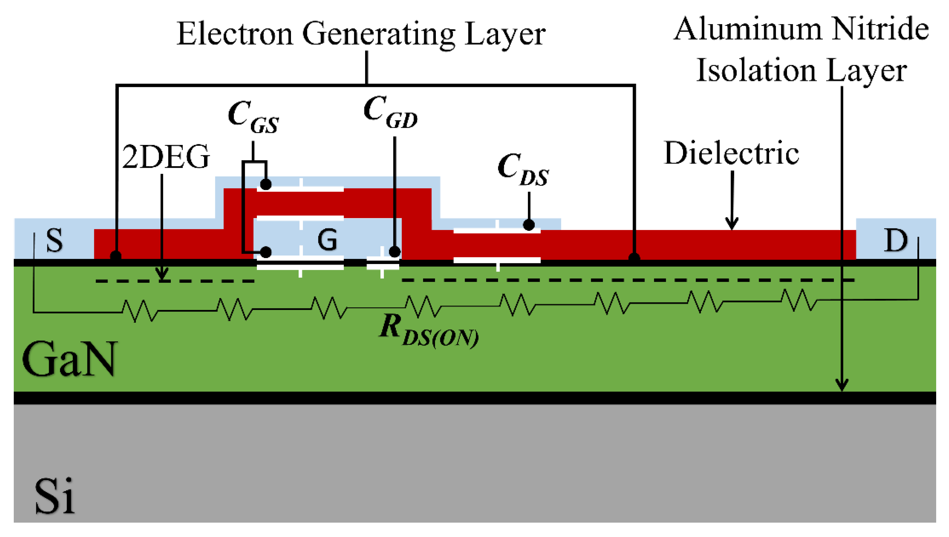
This paper is divided into the following sections: Section 2 will introduce the GaN structure studied in this paper. Section 3 will present the selection of static equations and the method for respective parameters extraction. Section 4 and Section 5 will verify the experimental static and dynamic characteristics, respectively. Section 6 will present the results of a double-pulse test (DPT) test to compare the effectiveness of the MOSFET LEVEL 3 model with the manufacturer model in LTSpice. Section 7 will conclude and foreshadow potential future work.

2. GaN Structure

The internal structure of a normally-off GaN-HEMT is shown in Figure 1 [22]. For HEMT fabrication on the silicon substrate, as is the case in the structure shown in Figure 1, aluminum nitride is used as a buffer layer to enable epitaxial growth of the active GaN layer. The formation of the two-dimensional electron gas (2-DEG) is achieved by the growth of a resistive AlGaN layer on top of the highly-resistive GaN layer. The transition from GaN to AlGaN creates polarization charge, which attracts mobile electrons that form the 2-DEG. To form a normally-off HEMT, which is required for power applications, the electrons under the gate are repelled by various techniques, such as embedding negative charge in the AlGaN layer and using gate materials with a suitable work function. Given that a positive gate voltage is needed to re-establish the 2-DEG under the gate, this region of the HEMT is analogous to a normally-off MOSFET. The gate-to-drain and gate-to-source regions are different from the MOSFET structure; however, they can be modeled as fixed drain and source resistances.
The switching ability of power devices depend on its parasitic capacitances, which are gate-to-source capacitance (CGS), gate-to-drain capacitance (CGD), and drain-to-source capacitance (CDS). The three parasitic capacitances, shown in Figure 1, are analogous to the parasitic capacitances in the MOSFET structure. An important quantitative difference is that the parasitic capacitances in HEMTs are much smaller, enabling operation at much higher switching frequencies. A major difference between GaN-HEMT and MOSFET is the lack of an intrinsic body diode. However, the intrinsic diode in MOSFET models can be easily eliminated by adopting zero values of its key parameters. Therefore, standard MOSFET equations can be applied to GaN-HEMTs.

3. Selection of Static Equations and Parameter Extraction

3.1. Selection of SPICE Equations

Modeling a GaN-HEMT requires mathematical equations for the drain current (ID) as a function of the applied gate-to-source (VGS) and drain-to-source (VDS) voltages. In SPICE, there are different sets of equations, referred to as model levels. LEVEL 1 is the simplest MOSFET model, which is based on the rudimentary device equations. Shah et al. [12] have used the equations of MOSFET LEVEL 1 to model GaN-HEMTs. However, their approach ignored the transfer characteristic for small VDS values, which in the case of any GaN-HEMT is impacted by the channel resistances outside the gate (these gate-to-source and gate-to-drain channel resistances do not exist in MOSFETs). In addition, the simulation accuracy of output characteristics is highly dependent on second-order effects, which are not included in [12]. The MOSFET LEVEL 2 model in SPICE includes second-order effects, but its equations are complex resulting in computational inefficiency and convergence issues. MOSFET LEVEL 3 is a much better choice, because its key equations are almost as simple as in MOSFET LEVEL 1 and as accurate as the complex equations in the MOSFET LEVEL 2 model. Therefore, the MOSFET LEVEL 3 model is utilized in this paper. In SPICE, a parameter labeled as LEVEL is assigned to MOSFET devices. By assigning LEVEL = 3, the SPICE LEVEL 3 model with the relevant equations and parameters is activated.
Equations (1) and (2), shown below, represent our selection from the rather complex MOSFET LEVEL 3 model, for the purpose of modeling GaN-HEMTs. The SPICE parameters that need to be specified to activate this selection are shown in the bold font. The list of these parameters is as follows: the transconductance parameter (KP), the threshold voltage (Vto), the channel length (L), the channel width (W), the drain resistance (Rd), the source resistance (Rs), the body-effect parameter (Gamma), the surface potential in strong inversion (Phi), and the mobility modulation constant (Theta). In this paper, we will also show that the subthreshold-current parameter (NFS) can be used to model the non-zero drain current for gate voltages below the threshold voltage. The default values of the remaining SPICE parameters ensure that all other equations are inactive [23].
I D = K P 1 + T h e t a ( V G S V t o ) W L ( V G S V t o ) ( V D S R s I D Rd I D ) [ 1 + Gamma 2 Phi ] ( V D S Rs I D Rd I D ) 2 2 Triode   Region
I D = KP 1 + Theta ( V G S Vto ) W L [ 2 Phi 2 ( 2 Phi + Gamma ) ] ( V G S Vto ) 2 ×   Saturation   Region

3.2. Methods for Extraction of Initial Values of the Selected Parameters

In principle, the values of equation parameters can be obtained by nonlinear fitting to experimental data. However, the convergence of nonlinear fitting entirely depends on the specified initial values of the equation parameters. More importantly, an inadequate choice of the initial values can lead to poor fitting. Hence, this paper proposes a method for extraction of the initial values of selected key parameters as the first step, followed by nonlinear fitting to adjust the values of all parameters in Equations (1) and (2).
The channel length and width, L and W, are the geometric-design parameters specific to the power device under test. For commercial power-semiconductor devices these values are undisclosed by the manufactures and are very hard to determine. However, for the purpose of circuit simulation, it is sufficient to set the value of W and L to 1 µm, which makes the ratio W/L = 1. That leaves the transconductance parameter KP as the active parameter whose value will determine the value of the drain current in response to the applied voltages. In addition to KP, the initial values of Vto, Rs, and Rd are also needed to enable successful nonlinear fitting. Therefore, the proposed method for the extraction of initial parameter values includes KP, Vto, Rs, and Rd. The values of the remaining parameters can be adjusted by nonlinear fitting using their typical or default values.

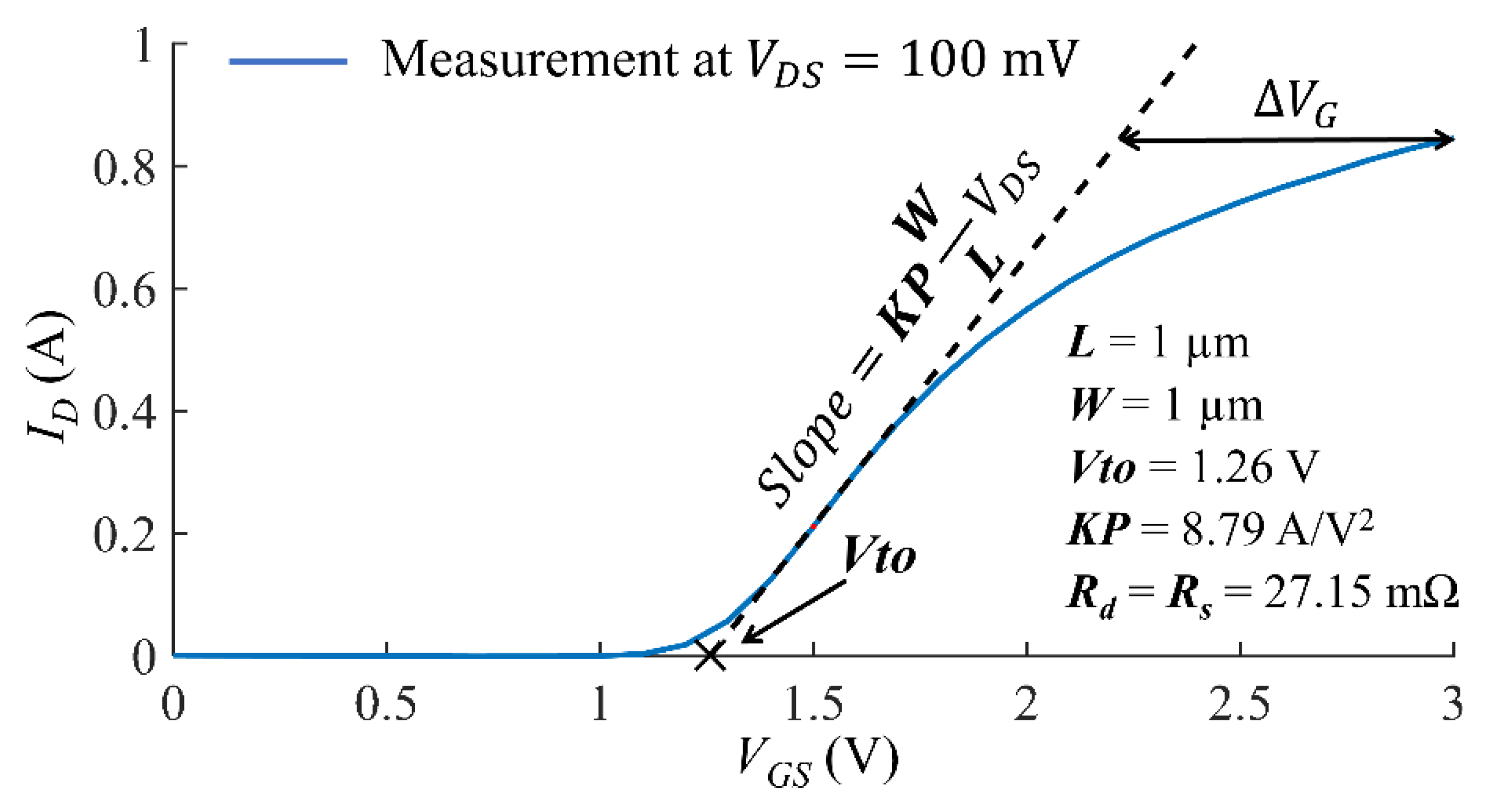
3.2.1. Extraction of KP, and Vto

The values of KP and Vto can be determined from measured transfer characteristic of the corresponding GaN-HEMT, biased in the linear region by a small VDS, such as VDS = 100 mV. To illustrate the extraction method, we chose a commercial 600 V GaN power transistor, GS66504B, manufactured by GaN Systems. The transfer characteristic of GS66504B was measured with an Agilent Power Device Analyzer (B1505A) and is shown in Figure 2. This transfer characteristic was measured at VDS = 100 mV to ensure that the quadratic term in (1) is negligible. In the linear section of the measured transfer characteristic, marked by the dashed line in Figure 2, the values of Theta(VGS-Vto), RsID, and RdID are negligible, simplifying (1) to the following linear form:
I D = KP ( W / L ) ( V G S Vto ) V D S
Equation (3) shows that the intersection between the extrapolated linear section of the measured transfer characteristic and the VGS axis that corresponds to Vto = 1.26 V. The slope of the linear section is 0.879 A/V, which corresponds to KP = 8.79 A/V2 for the specific case of VDS = 100 mV and W = L = 1 µm.

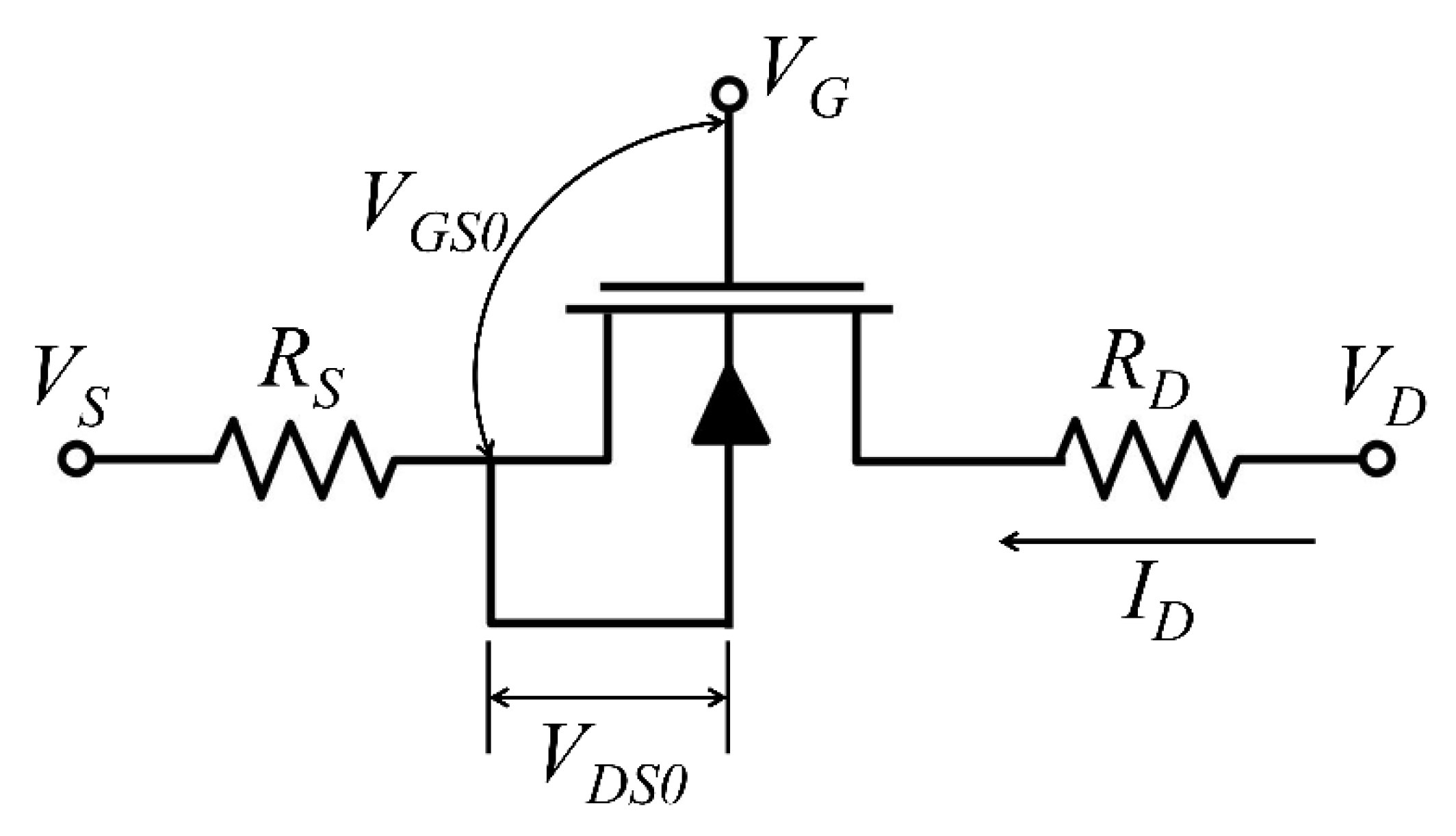
3.2.2. Extraction of Rs, and Rd

As Figure 2 shows, the measured transfer characteristic deviates from the linear dependence (the dashed line) for higher VGS and ID values, mainly due to the impact of the channel resistances outside the gate. MOSFET LEVEL 3 model has embedded source and drain resistances, Rs and Rd, which we can use to model the impact of gate-to-source and gate-to-drain channel resistances in HEMTs as shown in Figure 3. Assuming that the dashed line in Figure 2 corresponds to the HEMT channel under the gate, we can model this section of the channel by the linear equation:
I D = β ( V G S 0 Vto ) V D S 0
where, β = KP(W/L), VDS0 = VDS − (Rs + Rd) ID, and VGS0 = VGSRsID. From Equation (4), VGS0 can be expressed as:
V G S 0 = ( I D / β V D S 0 ) + Vto
For smaller ID values, where the solid and dashed lines overlap, (Rs + Rd) ID is negligible and VGS0 = VGS. However, for larger ID values, (Rs + Rd) ID is not negligible and a larger VGS is required to achieve the same ID. According to Equation (3), the measured value of VGS is given by
V G S = ( I D / β V D S ) + Vto
The difference ΔVG = VGS0VGS, which is illustrated in Figure 2, can be obtained from (5) and (6) as:
Δ V G = I D β [ 1 V D S ( Rs + Rd ) I D 1 V D S ]
Rs + Rd = V D S I D 1 ( I D / V D S ) + β Δ V G
Practically, a sufficiently high ID should be selected for the determination of Rs + Rd, because a sufficiently large ΔVG is needed to avoid a large error in the determined value for Rs + Rd. For the specific data shown in Figure 2, ΔVG = 0.8 V, VDS = 100 mV, ID = 0.84 A, and consequently Rs + Rd is obtained as 54.3 mΩ. For simplification of the model we assume equal drain and source resistances, which are Rs = Rd = 27.15 mΩ.

3.2.3. Typical Initial Values for Gamma, Phi, Theta, and NFS

Two parameters, Gamma and Phi, impact the drain current in the triode and saturation regions. The complete MOSFET LEVEL 3 equations in SPICE use Gamma and Phi to model second-order effects that we do not need in the case of HEMT modeling. As can be seen from the square brackets in Equations (1) and (2), it is sufficient to adjust the value of only one of these parameters. From semiconductor physics, we know that the value of Phi is set by the energy gap of the material. For the case of GaN, we can set Phi = 2 V, which leaves Gamma to be determined by the nonlinear fitting. For this purpose, the default value in SPICE, which is Gamma = 0, can be used as the initial value.
The default value for the parameter Theta in SPICE is also Theta = 0. This is sufficient as the initial value for the nonlinear fitting, which will adjust the final value of Theta to improve the fitting of both the transfer and the output characteristics. Finally, note that we can specify the parameter NFS to fit the subthreshold current on the transfer characteristic. The typical value of this parameter is 1011 cm−2. However, in the triode and saturation region, the NFS does not affect the ID as can be seen from Equations (1) and (2). Hence, the value of this parameter can be adjusted in SPICE simulation after the non-linear fitting is completed.

3.3. Non-Linear Fitting

Using the set values of W = L = 1 µm and Phi = 2 V, along with the initial values obtained in the previous sub-section (KP = 8.79 A/V2, Vto = 1.26 V, Rs = Rd = 27.15 mΩ) and the default values Theta = 0, and Gamma = 0, non-linear fitting is applied to Equations (1) and (2) to obtain the MOSFET LEVEL 3 parameters for GS66504B. The obtained fitted parameters are typed directly into SPICE and are verified by the experimental transfer and output characteristics as described in the next section. Note that, without NFS, the drain current calculated by SPICE will be zero for VGS < Vto. Hence, in order to fit the sub-threshold region for GS66504B, the value of NFS can be determined by running SPICE simulations with tried numbers around its typical value of 1011 cm−2.

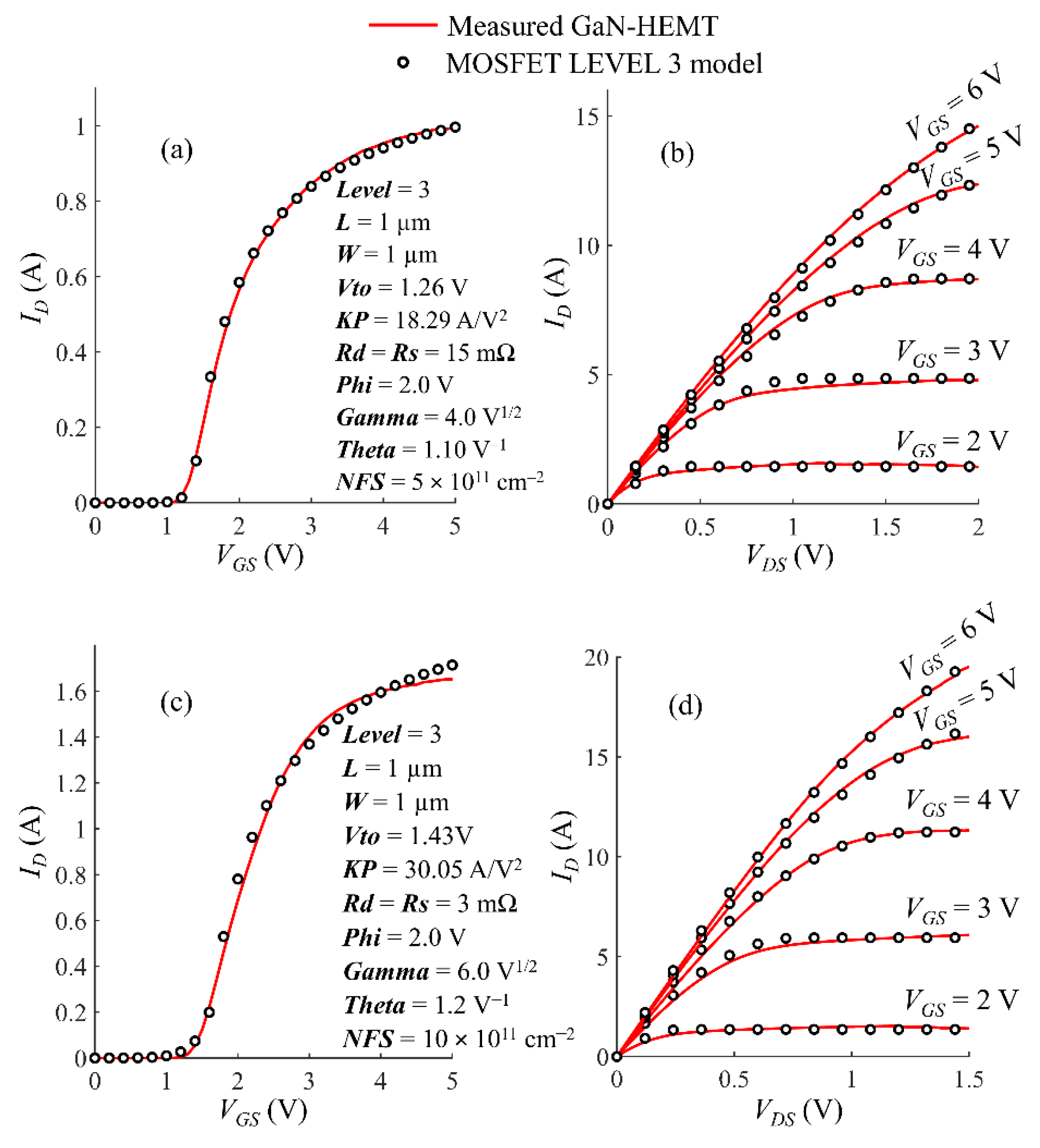
4. Experimental Verification of the Static Characteristics

In addition to GS66504B GaN-HEMT, we have also selected a 650 V GaN transistor GS66506T to demonstrate the effectiveness of the selected MOSFET LEVEL 3 equations and the proposed parameter-extraction method. Putting the fitted values of the selected parameters directly into SPICE, the simulated transfer and output characteristics for both GS66504B and GS66506T are compared with the measured results in Figure 4. It is evident that SPICE simulations are in very good agreement with the measured results, which demonstrates that the selected MOSFET LEVEL 3 equations in SPICE can be used to model GaN-HEMTs. Precise modeling in the linear region of the output characteristics, shown in Figure 4b,d, is the most significant, as it corresponds to the operation of HEMTs as switches in on mode and thus, determines the on-state resistance.

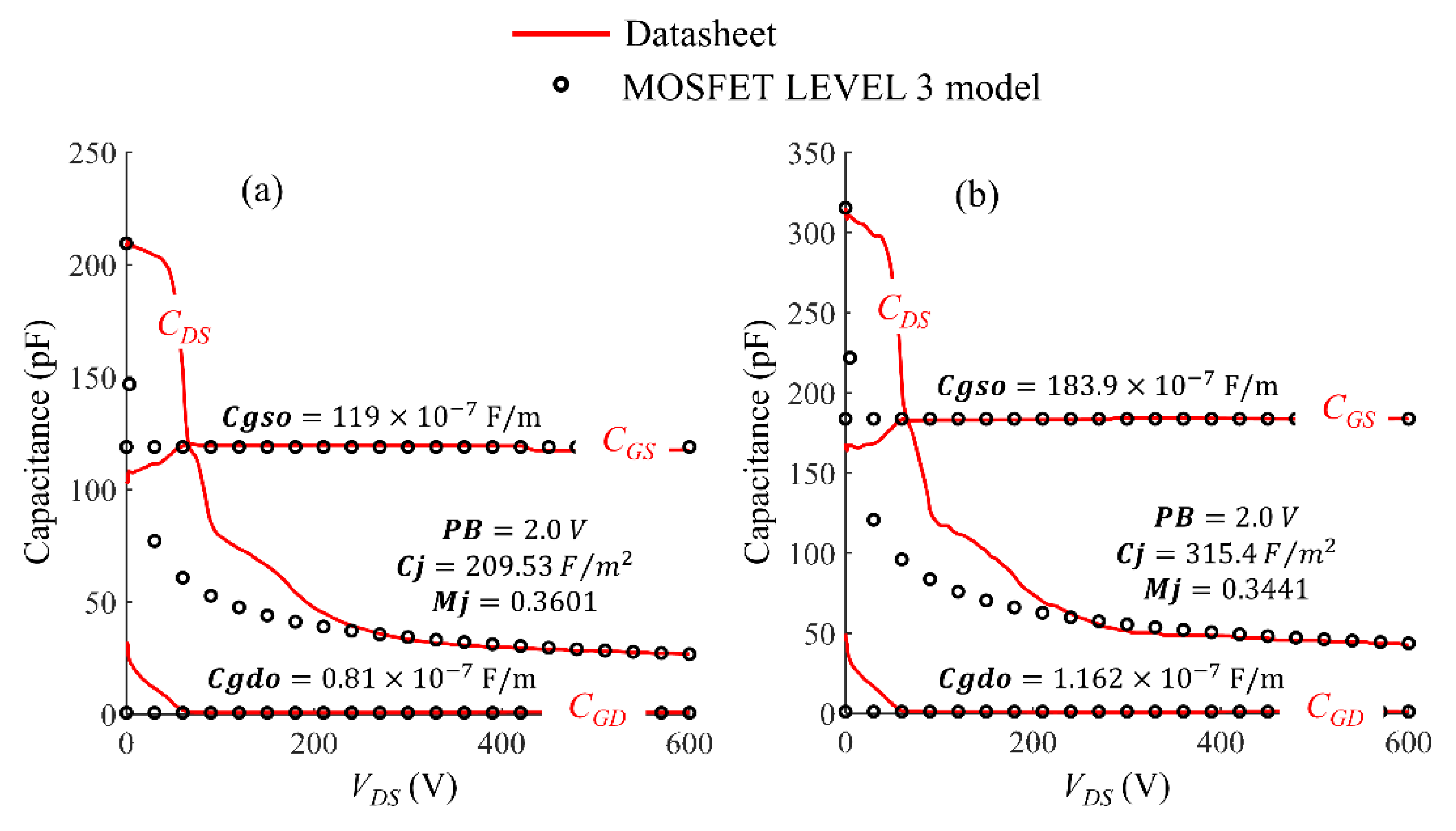
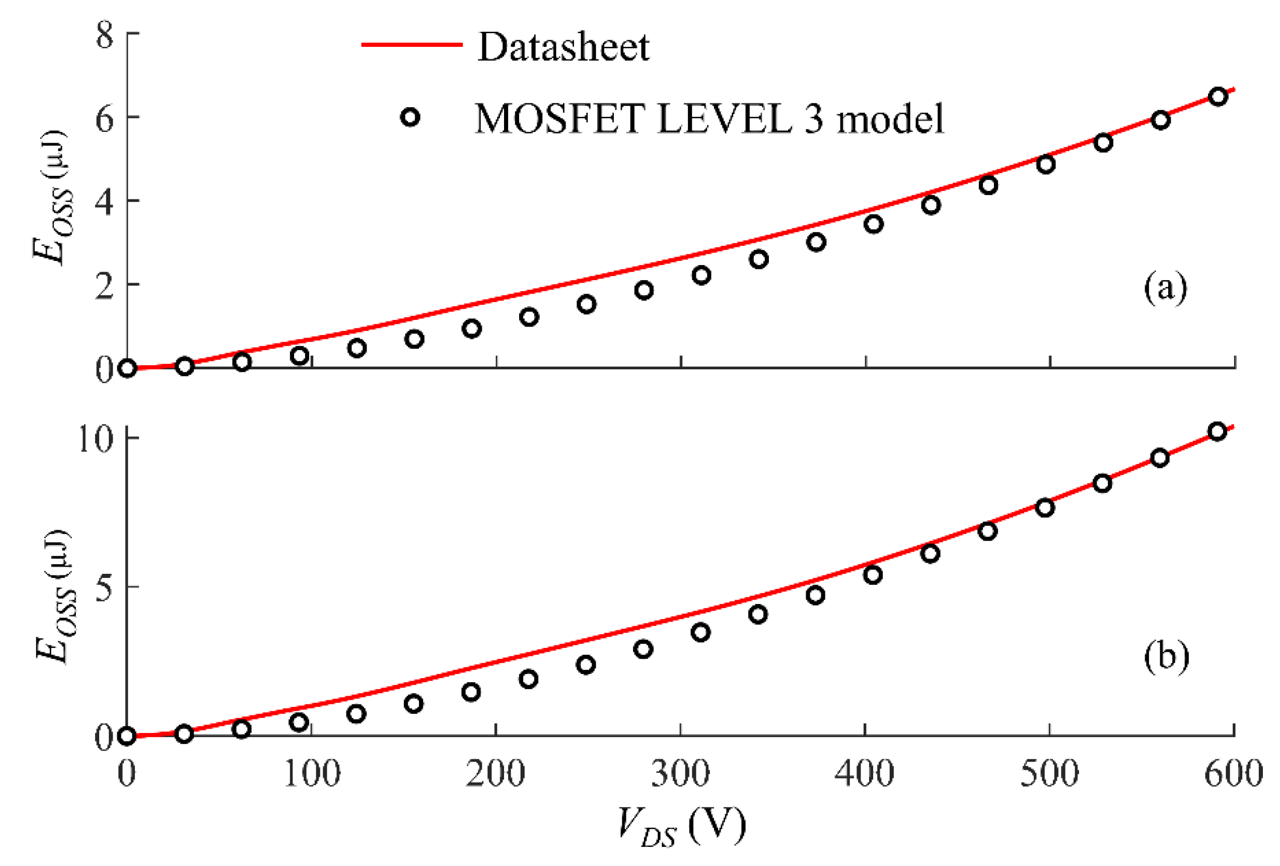
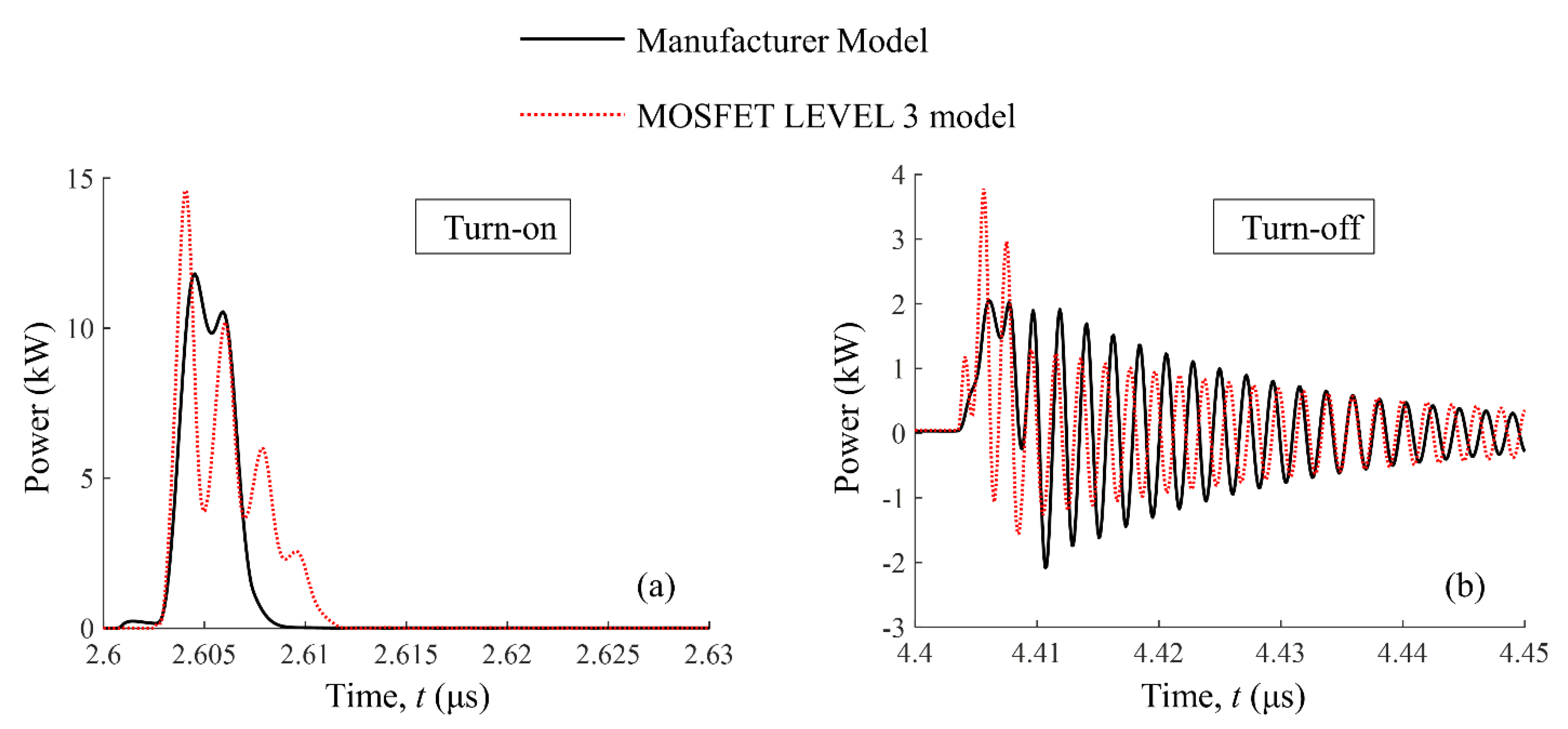
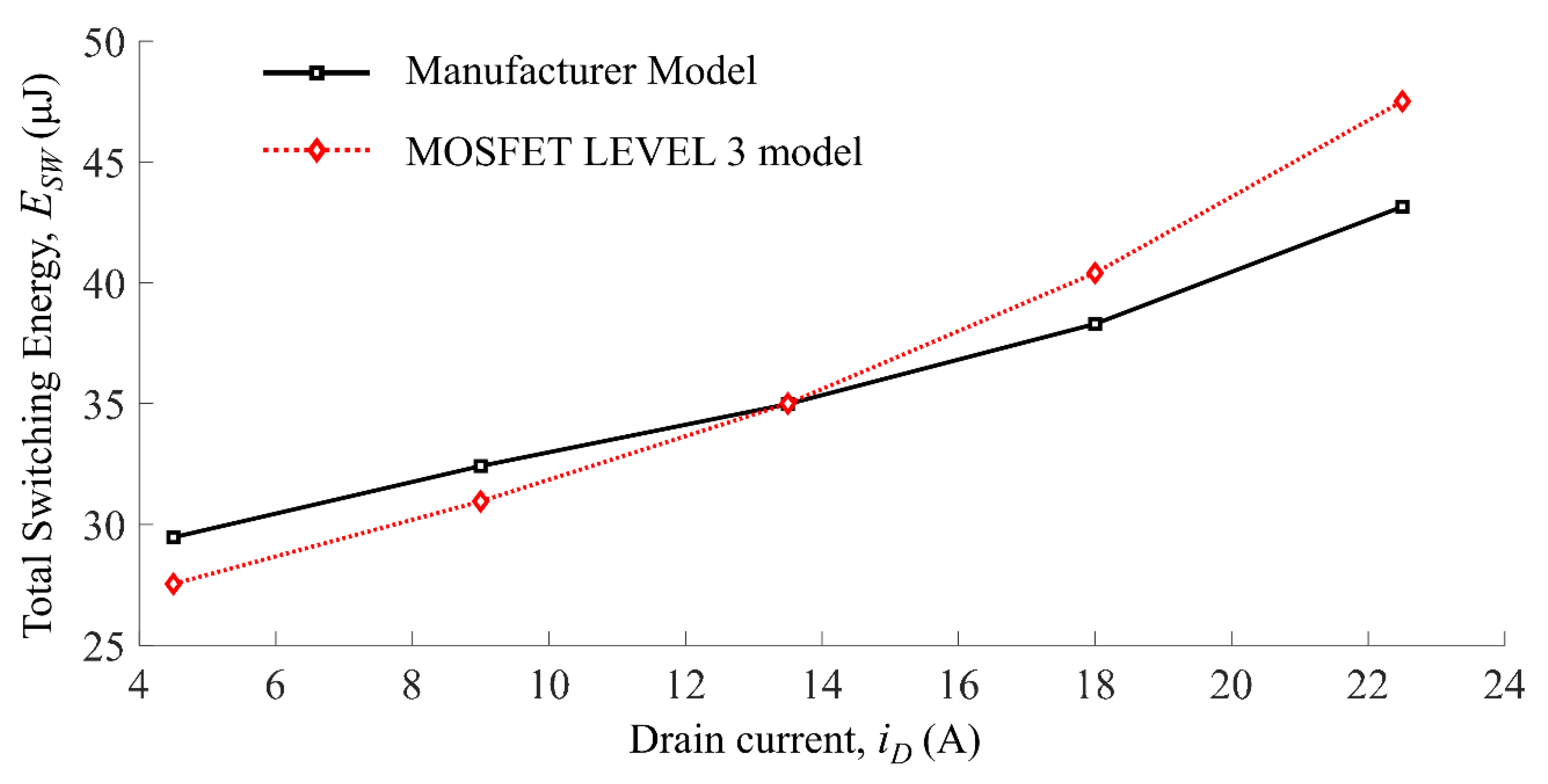
5. Modeling Dynamic Characteristics and Experimental Verification

The dynamic characteristics of GaN-HEMTs are determined by their inherent voltage-dependent parasitic capacitances. For the designers of power-conversion circuits, the capacitance of utmost interest is the output capacitance, COSS = CDS + CGD. Hence, modeling of CDS and CGD is crucial. The desired individual capacitance data from the datasheet is extracted using the grabit.m command in MATLAB and is shown in Figure 5.
The MOSFET LEVEL 3 model includes voltage-independent gate-to-source and gate-to-drain overlap capacitances, through Cgso and Cgdo as the respective parameters. By observing the datasheets of many GaN-HEMTs, it can be perceived that the CGS and CGD are fairly constant for most of the voltage ranges; hence the voltage-independent parameters Cgso and Cgdo can be used to model these capacitances. Note that Cgso and Cgdo are defined as capacitances per unit of the channel width. Therefore, extracting the values of Cgso and Cgdo can be achieved by taking the values of CGS and CGD at the maximum VDS.
The MOSFET LEVEL 3 model also contains a diode model for the MOSFET P‒N junction, which can be utilized to model the non-linear CDS for GaN-HEMTs. The diode model with relevant SPICE parameters is given by
C D S ( v D S ) = Cj [ 1 + ( v D S / PB ) ] M j
where, Cj is the zero-bias capacitance per unit area, PB is the built-in voltage, and Mj is the grading coefficient. To obtain the values of these SPICE parameters requires non-linear fitting. For this purpose, the CDS value from the datasheet at VDS = 0 V, should be divided by W × L and used as the initial value of Cj. The initial value of PB can be set at 2 V (similar to Phi) and the initial value of Mj can be set at 0.5 (typical value for one-sided abrupt P‒N junctions and Schottky diodes).
The modeled capacitances were compared to the extracted capacitance for both GaN-HEMTs in Figure 5. Good agreement is achieved at higher voltages, but there is a discrepancy between the simulated and datasheet CDS curves at lower voltages due to the internal physics of HEMTs.
The suitability of the capacitance modeling can be verified by comparing simulated and actual energy stored in the output capacitance (EOSS). This energy is stored while the GaN-HEMT is turning-off and the same energy is dissipated while the GaN-HEMT is turning-on. As high-frequency converters with GaN-HEMTs always require soft-switching, the EOSS curve is crucial for achieving this condition. The EOSS curve can be calculated from the respective COSS curve as:
E O S S = 0 V D S C O S S ( v D S ) × v D S d v D S
The EOSS curve calculated from Equation (10) for MOSFET LEVEL 3 modeling is compared to the datasheet and is shown in Figure 6. The results show that the proposed model is adequate for simple and fast simulation of HEMTs in power-electronic circuits.

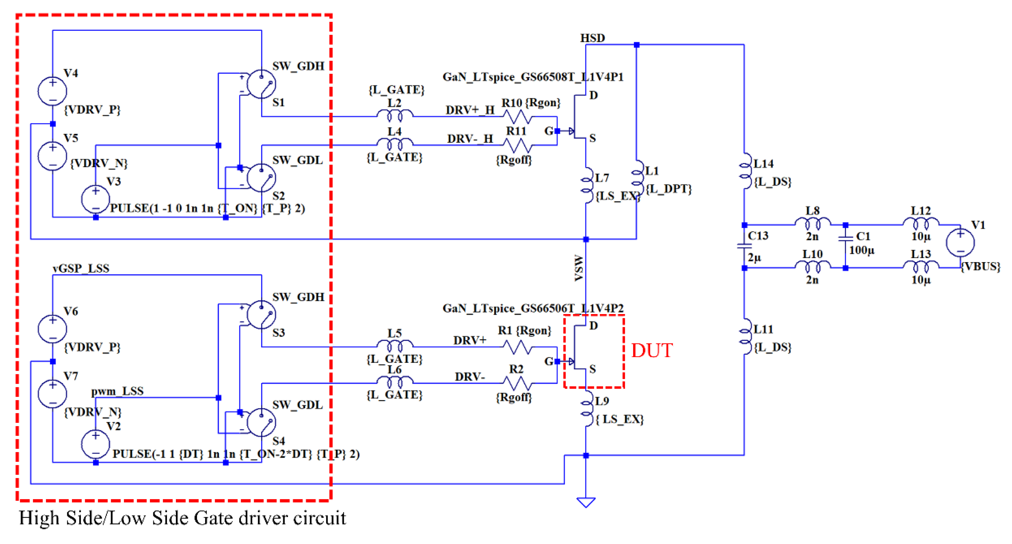
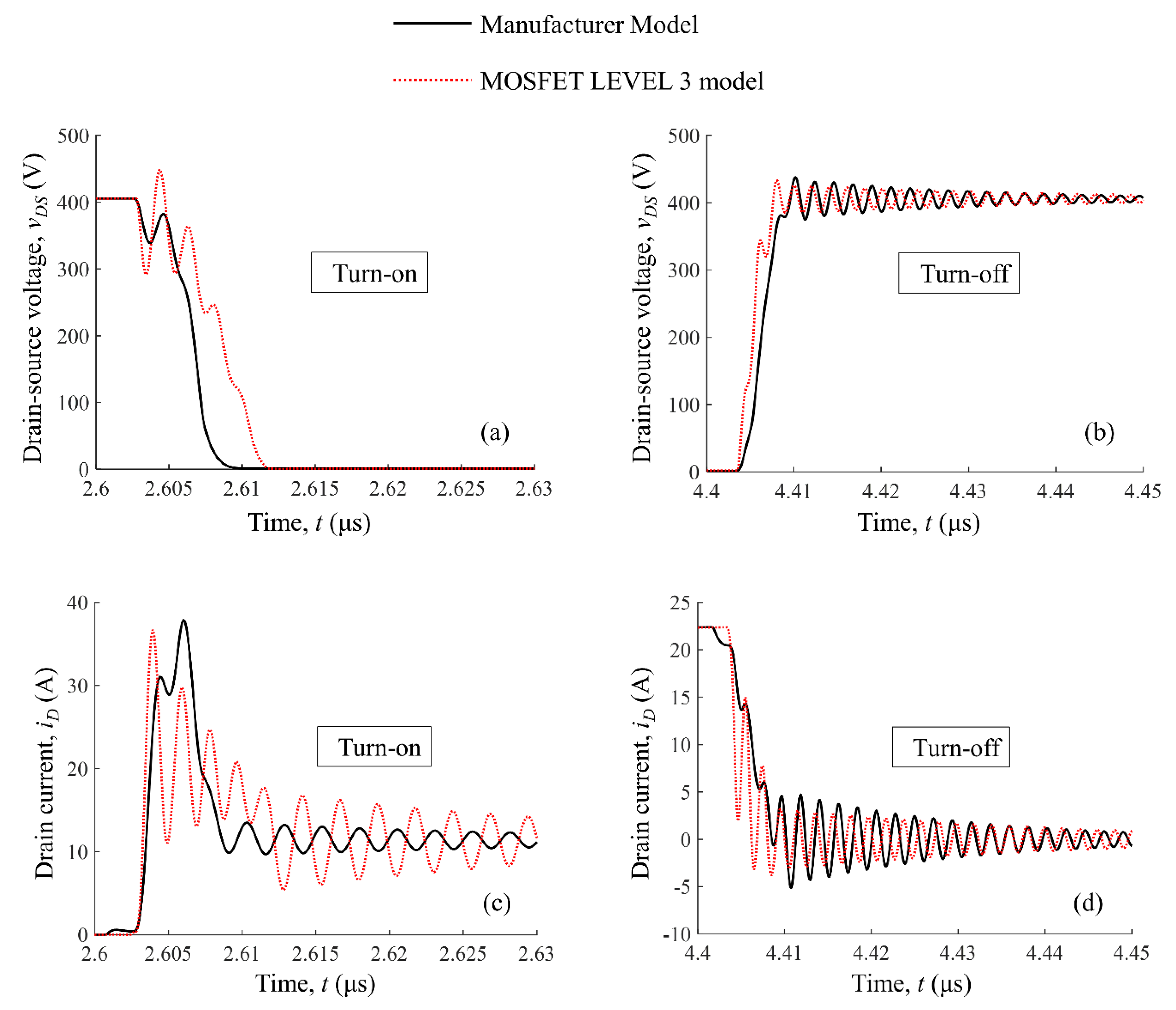
6. Model Validation by LTSpice Simulation

For power applications, a good way to validate the dynamic characteristics is to check how the developed model behaves under switching conditions. The manufacturer of GS66506T, GaN Systems, provides their own developed LTSpice model to be used for simulation purposes (the model is shown in Appendix A). Moreover, GaN Systems has developed a half-bridge double-pulse test (DPT) in LTSpice to evaluate the switching performance of their developed models in comparison to experimental measurements. As shown in the application notes [24], the manufacturer model is in good agreement with the experimental switching conditions. Hence, an identical double-pulse test platform developed by GaN Systems is used in this paper to verify the switching characteristics of the developed MOSFET LEVEL 3 model. Since LTSpice shares the same core libraries as any other SPICE version, the MOSFET LEVEL 3 model can be used in LTSpice simulation with adequately set parameter values, as shown in Appendix B. It is worth noting that two more parameters, namely, gate resistance (RG) and drain-to-source shunt resistance (RDS), are added while converting SPICE to LTSpice models to avoid convergence problem in LTSpice. The addition of these parameters does not have much effect on the electrical characteristics of the modeled GaN-HEMT. The value of RG is directly taken from the GS66506T datasheet as 1.1 Ω. The RDS is theoretically infinite; hence a very high value of 1 MΩ is used in the model. The DPT test bench in LTSpice is shown in Figure 7. The parameters of the DPT circuit along with their values are given in Table 1. The switching waveforms of the DPT circuit with both the manufacturer’s and MOSFET LEVEL 3 models as the device under test (DUT) are shown in Figure 8.
Figure 8a,b shows the results with an operating DC bus voltage of 400 V and Figure 8c,d shows the results with an operating switching current of 22.5 A. Despite the simplicity of MOSFET LEVEL 3 model, the turn-off transients shows satisfactory agreement with the manufacturer model, whereas a bigger difference can be seen in Figure 8a,c during turn-on transients for both operating points. This deviation during the turn-on interval is most likely caused by the mismatch of modeled CDS and CGD at lower voltages. In addition, the MOSFET LEVEL 3 model does not include any parasitic inductances, which results in more pronounced oscillations as seen in Figure 8. However, for power applications, the power distributions during switching intervals are more relevant. The turn-on and turn-off power losses using the MOSFET LEVEL 3 model and manufacturer model for the two operating points are shown in Figure 9. Furthermore, the total energy losses during switching transients are presented in Table 2.
Figure 9 and Table 2 demonstrate the effectiveness of the simple MOSFET LEVEL 3 model approach in comparison to the complex manufacturer model. Despite the observed deviation in the switching waveforms shown in Figure 8, the switching energy losses for the full current rating calculated from both models are quite close. In order to further evaluate the switching performance of the MOSFET LEVEL 3 model, the drain current was varied keeping the dc bus voltage constant and the comparison to the manufacturer model is shown in Figure 10. As can be seen, the simple MOSFET LEVEL 3 model provides adequate results in comparison to the complex manufacturer model. The observed variation between both curves in Figure 10 is acceptable in terms of designing power circuits, whereas the availability, transparency, and simplicity of the MOSFET LEVEL 3 model enables fast and effective simulations during the design of practical power-switching circuits.

7. Conclusions

This paper demonstrates that standard MOSFET equations, available in the SPICE circuit simulator, can be used to model commercial GaN-HEMTs. A set of equations from the available MOSFET LEVEL 3 equations in SPICE has been selected and a method for the extraction of the related SPICE parameters has been proposed. The validity of this approach, including the proposed parameter-extraction techniques, is verified by demonstrating an adequate match between simulated and measured static and dynamic characteristics. Furthermore, a DPT is performed for one of the GaN-HEMTs and is compared to its manufacturer model. It is demonstrated that the simple MOSFET LEVEL 3 model provides adequate results in terms of total switching energy losses. The transparency of the MOSFET LEVEL 3 model is further helpful in adapting to any GaN-HEMTs which is quite difficult in the manufacturer model. Due to the simplicity of this approach and the familiarity of circuit designs with the standard MOSFET SPICE model, this approach is ideally suited for the analysis and design of circuits with GaN-HEMTs. Future work may include an improvement of modeling of voltage-dependent capacitances to obtain switching energy losses as close as possible to the complex manufacturer model while keeping the model simple and transparent.

Author Contributions

Conceptualization, U.J. and S.D.; methodology, U.J., S.D., and F.M.-Y.; software, U.J.; validation, U.J., S.D., F.M.-Y., H.A.M., P.P., and M.C; formal analysis, U.J. and S.D.; investigation, U.J., S.D., F.M.-Y., H.A.M., and P.P; resources, S.D. and F.M.-Y.; data curation, U.J.; writing—original draft preparation, U.J. and S.D.; writing—review and editing, U.J., S.D., F.M.-Y., H.A.M., P.P., and M.C.; visualization, U.J., S.D.; supervision, S.D., F.M.-Y. and H.A.M.; project administration, S.D.; funding acquisition, S.D. and F.M.-Y. All authors have read and agreed to the published version of the manuscript.

Funding

This research was funded by the Innovative Manufacturing Cooperative Research Centre (IMCRC), and BlueGlass as the industry partner, grant number 220132.

Data Availability Statement

Data is contained within the article.

Acknowledgments

The authors would like to acknowledge the Innovative Manufacturing Cooperative Research Centre (IMCRC) for providing a PhD scholarship to the first author. We also acknowledge the School of Engineering and Built Environments (EBE) of Griffith University for funding this project. This work was performed in part at the Queensland node of the Australian National Fabrication Facility, a company established under the National Collaborative Research Infrastructure Strategy to provide nano- and micro-fabrication facilities for Australia’s researchers.

Conflicts of Interest

The authors declare no conflict of interest.

Appendix A

** GaN Systems Manufacturer model for GS66506T
*****************************************************************
.subckt GaN_LTspice_GS66506T_L1V4P2 gatein drainin sourcein
.param sf = 0.73
.param rTC = −0.004 gan_res = {44.75e−3} metal_res = {3.2e−3} gtc = 2.83 sh_s = 0.05263 sh_d = 0.94376
.param cur = 0.099 x0_0 = 1.1 x0_1 = 1.1 x0_2 = 1.0 thr = 1.61 itc = 0.42 atc = 90.8
rd drainin drain {sh_d * (metal_res/2.0 *(1-1*rTc*(Temp-25)) + gan_res*PWR((Temp + 273)/298,gtc))/sf }
rs sourcein source {sh_s * (metal_res/2.0 *(1-1*rTc*(Temp-25)) + gan_res*PWR((Temp + 273)/298,gtc))/sf }
rg gatein gate {1.0 * sf}
Rcsdconv drain source {4000Meg}
Rcgsconv gate source {4000Meg}
Rcgdconv gate drain {4000Meg}
bswitch drain2 source2 I = (if(v(drain2,source2) > 0,
+(cur*(-(Temp-25)*itc + atc)*log(1.0 + exp(26*(v(gate,source2)-thr)))*
+v(drain2,source2)/(1 + max(x0_0 + x0_1 *(v(gate,source2) + x0_2),0.2) *v(drain2,source2))),
+(-cur*(-(Temp-25)*itc + atc)*log(1.0 + exp(26*(v(gate,drain2)-thr)))*
+ v(source2, drain2)/(1 + max(x0_0 + x0_1*(v(gate,drain2) + x0_2),0.2)*v(source2,drain2))))) * sf
R_drain2 drain2 drain {(1e−4)}
R_source2 source2 source {(1e−4)}
C_GS gate source {228.3e−12 * sf}
C_GS1 gate source Q = sf * (−0.9431e−12*(1-1./(1 + exp(0.0177*(-v(drain, source) + 300.03))))
+ −0.4182e−10*(1-1./(1 + exp(0.0700*(-v(drain, source) + 33.3)))) + −0.5657e−10*(1-1./(1 + exp(0.277*(-v(drain, source) + 1.1))))
+ -(−0.435*90.48e−12*(1-1./(1 + exp(0.06*(-v(drain, source) + 1.1))))
+ −0.435*0.54e−10*(1-1./(1 + exp(0.9*(-v(drain, source) + 2.1))))))*x
C_GS2 gate source Q = 0.464*2.23e−010*log(1 + exp(6.5*(x-1.45))) * sf
C_GD gate drain {0.6e−012 * sf}
C_GD1 gate drain Q = 0.444*4.6e−10*log(1 + exp(0.277*(x + 1.1))) * sf + 0.444*13.2e−10*log(1 + exp(0.070*(x + 33.3))) * sf + 0.444*1.2e−10*log(1 + exp(0.0177*(x + 300.03))) * sf
C_SD source drain {0.8e−010 * sf}
C_SD1 source drain Q = 0.444*4.4e−9*log(1 + exp(.15*(x + 68))) * sf
+ 0.444*6.56e−9*log(1 + exp(.03*(x + 180))) * sf
.ends
*$

Appendix B

** MOSFET LEVEL 3 model for GS66506T
*****************************************************************
* Node 1 -> Drain
* Node 2 -> Gate
* Node 3 -> Source
.SUBCKT GS66506T 1 2 3
M2 9 7 8 8 MM L = 1U W = 1U
RS 8 3 3m
RD 9 1 3m
RG 2 7 1.1
RDS 3 1 1e6
.MODEL MM NMOS Level = 3
+Gamma = 6.0
+Theta = 1.20
+Phi = 2.0
+Kp = 30.05
+Vto = 1.43
+NFS = 10e11
+Cgso = 184e−7
+Cgdo = 1.162e−7
*Modeling drain-source-capacitance
D1 3 1 MD
.MODEL MD D
+CJO = 315.4e−12
+VJ = 2.0
+M = 0.3441
.ENDS GS66506T

References

  1. Mantooth, H.A.; Peng, K.; Santi, E.; Hudgins, J.L. Modeling of Wide Bandgap Power Semiconductor Devices—Part I. IEEE Trans. Electron Devices 2015, 62, 423–433. [Google Scholar] [CrossRef]
  2. Endruschat, A.; Novak, C.; Gerstner, H.; Heckel, T.; Joffe, C.; März, M. A Universal SPICE Field-Effect Transistor Model Applied on SiC and GaN Transistors. IEEE Trans. Power Electron. 2019, 34, 9131–9145. [Google Scholar] [CrossRef]
  3. Santi, E.; Peng, K.; Mantooth, H.A.; Hudgins, J.L. Modeling of Wide-Bandgap Power Semiconductor Devices—Part II. IEEE Trans. Electron Devices 2015, 62, 434–444. [Google Scholar] [CrossRef]
  4. Li, H.; Zhao, X.; Su, W.; Sun, K.; You, X.; Zheng, T.Q. Nonsegmented PSpice Circuit Model of GaN HEMT With Simulation Convergence Consideration. IEEE Trans. Ind. Electron. 2017, 64, 8992–9000. [Google Scholar] [CrossRef]
  5. Strauss, S.; Erlebach, A.; Cilento, T.; Marcon, D.; Stoffels, S.; Bakeroot, B. TCAD methodology for simulation of GaN-HEMT power devices. In Proceedings of the IEEE 26th International Symposium on Power Semiconductor Devices & IC’s (ISPSD), Waikoloa, HI, USA, 15–19 June 2014; pp. 257–260. [Google Scholar] [CrossRef]
  6. Huang, H.; Liang, Y.C.; Samudra, G.S. Theoretical calculation and efficient simulations of power semiconductor AlGaN/GaN HEMTs. In Proceedings of the IEEE International Conference on Electron Devices and Solid State Circuit (EDSSC), Bangkok, Thailand, 3–5 December 2012; pp. 1–4. [Google Scholar] [CrossRef]
  7. Waldron, J.; Chow, T.P. Physics-based analytical model for high-voltage bidirectional GaN transistors using lateral GaN power HEMT. In Proceedings of the 25th International Symposium on Power Semiconductor Devices & IC’s (ISPSD), Kanazawa, Japan, 26–30 May 2013; pp. 213–216. [Google Scholar] [CrossRef]
  8. Syamal, B.; Zhou, X.; Chiah, S.B.; Jesudas, A.M.; Arulkumaran, S.; Ng, G.I. A Comprehensive Compact Model for GaN HEMTs, Including Quasi-Steady-State and Transient Trap-Charge Effects. IEEE Trans. Electron Devices 2016, 63, 1478–1485. [Google Scholar] [CrossRef]
  9. Li, M.; Wang, Y. 2-d analytical model for current -voltage characteristics and transconductance of algan/gan modfets. IEEE Trans. Electron Devices 2008, 55, 261–267. [Google Scholar] [CrossRef]
  10. Krantia, A.; Haldarb, S.; Gupta, R.S. An accurate charge control model for spontaneous and piezoelectric polarization dependent two-dimensional electron gas sheet charge density of lattice-mismatched algan/GaN hemts. Solid State Electron. 2002, 46, 621–630. [Google Scholar] [CrossRef]
  11. Yu, T.-H.; Brennan, K.F. Theoretical study of a GaN-AlGaN high electron mobility transistor including a nonlinear polarization model. IEEE Trans. Electron Devices 2003, 50, 315–323. [Google Scholar] [CrossRef]
  12. Shah, K.; Shenai, K. Simple and Accurate Circuit Simulation Model for Gallium Nitride Power Transistors. IEEE Trans. Electron Devices 2012, 59, 2735–2741. [Google Scholar] [CrossRef]
  13. Aghdam, G.H. Model characterization and performance evaluation of GaN FET in DC-DC POL regulators. In Proceedings of the 2015 IEEE International Telecommunications Energy Conference (INTELEC), Osaka, Japan, 18–22 October 2015; pp. 1–4. [Google Scholar] [CrossRef]
  14. Huang, X.; Li, Q.; Liu, Z.; Lee, F.C. Analytical loss model of high voltage GaN hemtin cascode configuration. IEEE Trans. Power Electron. 2014, 29, 2208–2219. [Google Scholar] [CrossRef]
  15. DasGupta, N.; DasGupta, A. A new SPICE MOSFET Level 3-like model of HEMT’s for circuit simulation. IEEE Trans. Electron Devices 1998, 45, 1494–1500. [Google Scholar] [CrossRef]
  16. Peng, K.; Eskandari, S.; Santi, E. Characterization and Modeling of a Gallium Nitride Power HEMT. IEEE Trans. Ind. Appl. 2016, 52, 4965–4975. [Google Scholar] [CrossRef]
  17. Bouchour, A.M.; Dherbécourt, P.; Echeverri, A.; Oualkadi, A.E.; Latry, O. Modeling of Power GaN HEMT for Switching Circuits Applications Using Levenberg-Marquardt Algorithm. In Proceedings of the International Symposium on Advanced Electrical and Communication Technologies (ISAECT), Rabat, Morocco, 21–23 November 2018; pp. 1–6. [Google Scholar] [CrossRef]
  18. Xie, R.; Wang, H.; Tang, G.; Yang, X.; Chen, K.J. An analytical model for false turn-on evaluation of high-voltage enhancement-mode GaN transistor in bridge-leg configuration. IEEE Trans. Power Electron. 2016, 32, 6416–6433. [Google Scholar] [CrossRef]
  19. Hari, N.; Ramasamy, S.; Ahsan, M.; Haider, J.; Rodrigues, E.M.G. An RF Approach to Modelling Gallium Nitride Power Devices Using Parasitic Extraction. Electronics 2020, 9, 2007. [Google Scholar] [CrossRef]
  20. Islam, S.S.; Anwar, A.F.M. SPICE model of AlGaN/GaN HEMTs and simulation of VCO and power amplifier. In Proceedings of the IEEE Lester Eastman Conference on High Performance Devices, Troy, NY, USA, 4–6 August 2004; pp. 229–235. [Google Scholar] [CrossRef]
  21. Zeltser, I.; Ben-Yaakov, S. On SPICE Simulation of Voltage-Dependent Capacitors. IEEE Trans. Power Electron. 2018, 33, 3703–3710. [Google Scholar] [CrossRef]
  22. Colino, S.; Beach, R. Fundamentals of Gallium Nitride Power Transistors; Efficient Power Conversion Corp.: El Segundo, CA, USA, 2009; Application Note. [Google Scholar]
  23. Dimitrijev, S. MOSFET. Principles of Semiconductor Devices, 2nd ed.; Oxford University Press: New York, NY, USA, 2012; pp. 312–316. [Google Scholar]
  24. GaN Systems. Available online: https://gansystems.com/wp-content/uploads/2018/05/GN008-GaN_Switching_Loss_Simulation_LTspice_20180523.pdf (accessed on 1 October 2020).
Figure 1. Internal cross-sectional structure of a gallium nitride based high-electron-mobility-transistor (GaN-HEMT).
Electronics 10 00130 g001
Figure 2. Extraction of KP, Vto, Rs, and Rd from measured transfer characteristic of GS66504B GaN-HEMT.
Electronics 10 00130 g002
Figure 3. Equivalent circuit consisting of source and drain resistance for modeling GaN-HEMT.
Electronics 10 00130 g003
Figure 4. Verification of MOSFET LEVEL 3 model for GS66504B using measured (a) transfer characteristics and (b) output characteristics. Verification of MOSFET LEVEL 3 model for GS66506T using measured (c) transfer characteristics and (d) output characteristics.
Electronics 10 00130 g004
Figure 5. Verification of dynamic characteristics of MOSFET LEVEL 3 model for (a) GS66504B and (b) GS66506T.
Electronics 10 00130 g005
Figure 6. Energy stored in the output capacitance for (a) GS66504B and (b) GS66506T.
Electronics 10 00130 g006
Figure 7. Double-pulse test circuit in LTSpice simulation.
Electronics 10 00130 g007
Figure 8. Simulated switching waveform obtained with the MOSFET LEVEL 3 model in comparison to the manufacturer model; (a,c) are showing drain-to-source voltage and drain current waveforms for the turn-on interval, whereas (b,d) are showing drain-to-source voltage and drain current waveforms for the turn-off interval.
Electronics 10 00130 g008
Figure 9. Simulated power comparison between manufacturer model and the MOSFET LEVEL 3 model during (a) turn-on interval and (b) turn-off interval.
Electronics 10 00130 g009
Figure 10. Comparison of total switching energy losses for different drain currents.
Electronics 10 00130 g010
Table 1. Parameters of the double-pulse test (DPT) circuit used for LTSpice simulation.
S. No.ParametersValue
SymbolDescription
1VBUSDC bus voltage400 V
2ISWSwitching current22.5 A
3RGONTurn-on gate resistor10 Ω
4RGOFFTurn-off gate resistor2 Ω
5VDRV_PTurn-on gate voltage6 V
6VDRV_NTurn-off gate voltage2 V
7DTDead time100 ns
8T_ONTurn-on period2 μs
9T_PTotal period2.5 μs
10L_DPTSwitching current inductance64 μH
11L_GATEGate inductance1 nH
12LS_EXExternal source inductance10 pH
13L_DSPower loop inductance1 nH
Table 2. Energy losses during switching transients.
Energy   Losses   E = t 1 t 2 ( v D S    ×    i D )    d t Manufacturer ModelMOSFET LEVEL 3 Model
EON35.92 μJ42.50 μJ
EOFF7.23 μJ5.05 μJ
ESW = EON + EOFF43.15 μJ47.55 μJ
Publisher’s Note: MDPI stays neutral with regard to jurisdictional claims in published maps and institutional affiliations.

