Article

AC Current Ripple Harmonic Pollution in Three-Phase Four-Leg Active Front-End AC/DC Converter for On-Board EV Chargers

Department of Electrical, Electronic, and Information Engineering, University of Bologna, 40136 Bologna, Italy
*
Author to whom correspondence should be addressed.
Electronics 2021, 10(2), 116; https://doi.org/10.3390/electronics10020116
Submission received: 30 November 2020 / Revised: 31 December 2020 / Accepted: 1 January 2021 / Published: 7 January 2021
(This article belongs to the Section Electrical and Autonomous Vehicles)

Abstract

:
Three-phase four-leg voltage-source converters have been considered for some recent projects in smart grids and in the automotive industry, projects such as on-board electric vehicles (EVs) chargers, thanks to their built-in ability to handle unbalanced AC currents through the 4th wire (neutral). Although conventional carrier-based modulations (CBMs) and space vector modulations (SVMs) have been commonly applied and extensively studied for three-phase four-leg voltage-source converters, very little has been reported concerning their pollution impact on AC grid in terms of switching ripple currents. This paper introduces a thorough analytical derivation of peak-to-peak and RMS values of the AC current ripple under balanced and unbalanced working conditions, in the case of three-phase four-leg converters with uncoupled AC-link inductors. The proposed mathematical approach covers both phase and neutral currents. All analytical findings have been applied to two industry recognized CBM methods, namely sinusoidal pulse-width modulation (PWM) and centered PWM (equivalent to SVM). The derived equations are effective, simple, and ready-to-use for accurate AC current ripple calculations. At the same time, the proposed equations and diagrams can be successfully adopted to design the conversion system basing on the grid codes in terms of current ripple (or total harmonic distortion (THD)/total demand distortion (TDD)) restrictions, enabling the sizing of AC-link inductors and the determination of the proper switching frequency for the given operating conditions. The analytical developments have been thoroughly verified by numerical simulations in MATLAB/Simulink and by extensive experimental tests.

1. Introduction

Three-phase four-wire voltage-source converters (VSCs) are becoming increasingly popular in different power applications, such as grid-connected generation systems [1,2], shunt active power filters [3], active front-end rectifiers [4], renewable energy sources, and electric drives [5] applications. Moreover, this kind of topology has started to be widely adopted as active front-end of dual stage electric vehicle (EV) battery on-board chargers (OBCs) in order to enable vehicle-to-grid (V2G), vehicle-for-grid (V4G) and vehicle-to-X (V2X) services [6,7]. The growing interest in this converter structure is mainly due to its capability to support bidirectional power flow and its built-in feature to absorb/inject unbalanced three-phase currents. The latter property is useful to compensate unbalanced loads in local weak grids, functioning as a power conditioner. Different topologies can be found in the literature: split capacitor with [8] and without [9,10] neutral inductor, four-leg with [11] and without [6] neutral inductor, and independently controlled neutral module [12,13].
The most adopted modulation strategies to control three-phase four-wire converters are carrier-based pulse-width modulation (CBPWM) [14] and space vector modulation (SVM) [15]. They have been broadly employed thanks to their simple implementation, fixed switching frequency, and well-known harmonic spectrum [16,17]. These features assist the evaluation of the switching losses, which allows the converter design to be more accurate.
The modulation technique directly affects different converters’ characteristics, particularly the AC current ripple propagating on the grid supply in the case of an OBC. The determination of the current ripple is crucial for a proper design of a power electronic-based conversion system in terms of reactive components (AC grid filters), losses, and its overall efficiency evaluation. Moreover, AC current ripple minimization can lead to an increase in the efficiency and reliability of the whole EV charger. However, prior to the aforementioned design steps, the AC current ripple must be well examined, deriving its complete mathematical formulation. An exhaustive study of the peak-to-peak current ripple as a function of the modulation index has been provided for three-phase three-leg PWM converters [18]. Moreover, there is a comparative study of the peak-to-peak current ripple for two-level and multilevel PWM converters [19]. The importance of the current ripple distribution over a fundamental period (i.e., the ripple envelope) has been highlighted in different papers [20,21]. The knowledge of current ripple distribution allows estimating many operational features of the converter, such as the switching ripple average, peak, RMS, and the zero-crossing intervals, leading to a more precise compensation of the dead-time effects in VSC schemes [21].
Researchers from the cited studies have mainly focused their attention on the peak-to-peak current ripple for three-phase three-leg PWM converters. Concerning three-phase four-leg VSCs, the maximum AC current ripple has been already examined and compared with the case of three-leg converters [6]. However, the analysis has not been extended to the neutral current ripple, no analytical expression of the envelops has been provided, and current ripple RMS has not been carried out. A general method to design the neutral line inductor has been proposed for the same topology [22]. The peak-to-peak current ripple and its maximum value were calculated analytically; however, only the sinusoidal PWM (SPWM) has been considered [23]. Different works have examined the four-leg topology with the aim to achieve higher working efficiency. For example, a new carrier-based PWM technique has been presented [24]. It is based on an injection of the opposite median voltage as a zero-sequence voltage, leading to a loss reduction in the three-phase four-wire converter. Hou et al. adopted the multicarrier PWM with the aim to reduce the common mode voltage and current [25]. Mandrioli et al. performed an exhaustive analytical description of the phase and neutral current ripple characteristics in three-phase four-leg grid-connected inverters without neutral line inductor for the most popular discontinuous PWM (DPWM) [26].
To the best of the authors’ knowledge, no works so far have provided a complete AC phase and neutral current ripple analysis for three-phase four-leg VSCs applying either sinusoidal or centered PWMs under balanced and unbalanced modulating conditions, apart from the analysis for SPWM [23]. Moreover, in the same paper, the significance of secondary AC current ripple was highlighted. Its accounting permits one to obtain an accurate expression for RMS value of phase current ripple. The aim of this paper is to extend the analysis introduced by Viatkin et al. [23] that has been done only for SPWM, and to present a complete mathematical formulation of envelopes and RMS values of AC current switching ripple when a general PWM strategy is adopted. In this way, the given expressions in a generic form might be exploited for a PWM technique with any abstract injection. The AC current ripple examination has been performed for the four-leg VSC architecture with interface inductors placed solely in phases (three inductor arrangement). Other popular three-phase four-wire VSI configurations (e.g., mentioned above) are outside the scope of this paper. The theoretical findings are validated through both numerical simulations and experiments. The achieved results show an adequate match with the analytical developments.
The significant contributions of this paper are: (1) complete mathematical analysis of the AC current ripple (defining primary and secondary envelops) for four-leg VSC in the case of general PWM with particular attention on the SPWM and centered PWM (CPWM, equivalent to SVM); (2) development of straightforward mathematical equations for peak and peak-to-peak profiles of the phase and neutral current ripples under balanced and unbalanced working conditions; (3) formation of simple, highly accurate expressions for the RMS evaluation of the phase and neutral current ripples under balanced operation; (4) comparative examination of the AC current ripple between SPWM and CPWM in the four-leg architecture, as well as with their analogies from a three-leg VSC.
All analytical equations have been derived in a short and well-defined form as functions either modulation index or modulation index and phase angle. They are especially handy for converter design processes, providing an accurate result without the need to run heavy repetitive numerical simulations. For instance, having knowledge about input design parameters, such as DC voltage level, switching frequency, modulation method, and restricted current ripple characteristics (peak-to-peak or/and RMS values) one can easily size the ac interfacing inductors. Alternatively, bearing in mind the design parameters of a power converter, one can compute TDD or THD at a specific operating point to check the compliance with the associated standard.
The paper is organized as follows. The basic assumptions and the adopted modulation principle are introduced in Section 2. The analysis of the phase current ripple and the evaluation of RMS values for both balanced and unbalanced cases is presented in Section 3. Similar investigation for the neutral is introduced in Section 4 and experimental results are given in Section 5. Comparison and detailed interpretation of obtained results is reported in Section 6. Finally, the overall significance of current study is highlighted in Section 7.

2. Basic Assumptions and Modulation Principle

2.1. Converter Model and Current Ripple Definition

The investigated front-end converter configuration for OBC consists of four identical legs, each of them made up of two switches, as shown in Figure 1. The AC phase terminals are linked to grid by three magnetically independent inductors (L). The middle point (n) of the fourth leg is directly linked with the common neutral point of the supply grid.
Referring to Figure 1, v x represents generic converter’s instantaneous phase voltage, and i x is the instantaneous phase current. Both v x and i x can be written in terms of spectral components as:
{ v x ( t ) = v ¯ x ( t ) + v ^ x ( t ) i x ( t ) = i ¯ x ( t ) + i ^ x ( t )
where v ¯ x and i ¯ x are the fundamental (low-frequency) components (i.e., averaged over a switching period Tsw), and v ^ x and i ^ x are the switching (high-frequency) ripple components.
It is easy to demonstrate that the drop in resistive voltage due to current ripple i ^ x flow is negligible in comparison with the voltage ripple component v ^ x (the latter has an amplitude in the order of Vdc):
v ^ x ( t ) L d i ^ x ( t ) d t
As commonly accepted, the instantaneous current ripple can be computed by replacing Equation (1) in Equation (2) and integrating over any generic period (t), leading to:
i ^ x ( t ) i ^ x ( 0 ) 1 L 0 t v ^ x ( t ) d t = 1 L 0 t [ v x ( t ) v ¯ x ( t ) ] d t
The magnitude of the peak-to-peak current ripple over a switching period Tsw can be defined as:
i ^ x , p p ( t ) = max { i ^ x ( t ) } 0 T s w min { i ^ x ( t ) } 0 T s w
The converter voltage v x , which is the voltage between converters’ terminals x and n, is expressed as:
v x ( t ) = V d c [ g x ( t ) g n ( t ) ]
where gx and gn are converter pole voltages normalized by Vdc in phase leg x and neutral leg n, respectively. Objectively, the three converters’ voltages correspond to AC voltages of three H-bridges sharing one of the two legs (i.e., the 4th leg). Therefore, these voltages can be treated as independent of each other.

2.2. Carrier-Based Pulse-Width Modulation

In this subsection, the mathematical representation of a generic carrier-based pulse-width modulation is reported. Although the presented equations are valid for a large number of well-known PWM-based techniques, in this paper the attention has been paid to the most employed strategies, namely SPWM and CPWM (equivalent to SVM). Therefore, all supporting figures are depicted with reference to these two modulation methods.
For four-leg PWM converters, the three modulating signals u x * are composed by the sinusoidal phase reference voltages normalized by Vdc (ux) and an additive common mode signal γ(t) (if any), while the modulating signal un, for the 4th leg, is solely given by the common mode signal γ(t) (if any, otherwise 0):
{ u x * ( t ) = u x ( t ) + γ ( t ) = m x cos ( ϑ x ) + γ ( t )     u n ( t ) = γ ( t )
being x the phase index (a, b, c); ϑx = ωt + φx, where φx is the phase angles, ω the fundamental angular frequency; and mx the modulation index defined as
m x = 2 V x V d c
where Vx is the RMS value of the reference phase voltage. In the case of balanced modulation (with or without injection) ma = mb = mc = m, and ϑa = ϑ = ωt, ϑb = ϑ 2π/3, ϑc = ϑ + 2π/3. The carrier range is ± 0.5. Therefore, linear modulation range for SPWM is limited to m = [0, 0.5] and for CPWM is m = [0, 1/√3].
In case of SPWM, the common mode signal γ(t) is zero:
γ ( t ) = 0
In case of CPWM, the common mode signal γ(t) is:
γ ( t ) = 1 2 [ m a x ( u a , u b , u c ) + m i n ( u a , u b , u c ) ]
In balanced condition and thanks to the half-wave symmetry, Equation (9) can be shortened to:
γ ( m , ϑ ) = m 2 cos ( ϑ + π 3 ) , 0 ϑ π 3  
A generic PWM pattern is depicted in Figure 2. The modulating signals ( u a * , u b * , u c * , and u n ) within an arbitrary switching period are also illustrated. Here, it is convenient to calculate the switching time slots (t0, t1, and t2) for the falling carrier edge with reference to the half of a switching period. Due to symmetry of the triangular carrier, these time intervals are identical to their counterparts for positive carrier slope. The depicted quantities (phase voltage and current) in Figure 2 are made with the reference to phase a when the corresponding modulating signal is positive.
By assuming the switching period small enough to consider the modulating signals constant within it, the time intervals can be calculated as:
{ t 0 = T s w 2 ( 1 2 u x * ( t ) ) = T s w 2 ( 1 2 u x ( t ) γ ( t ) ) t 1 = T s w 2 ( u x * ( t ) u n ( t ) ) = T s w 2 u x ( t ) t 2 = T s w 2 ( 1 2 + u n ( t ) ) = T s w 2 ( 1 2 + γ ( t ) )
Independently from the injection, the average converter voltage over the switching period is given by:
v ¯ x ( t ) = V d c [ u x * ( t ) u n ( t ) ] = V d c u x ( t )
By introducing Equations (12) and (5) in Equation (1), the ripple voltage component can be written as:
v ^ x ( t ) = V d c [ g x ( t ) g n ( t ) ] V d c u x ( t )

3. Analysis of Phase Currents Ripple

3.1. Phase Current Ripple Waveform

To determine the current (switching) ripple, only intervals t0 and t2 can be considered. By introducing Equations (11) and (12) into Equation (3) and simplifying, one can eventually obtain the two local extrema of the current ripple in phase x (for ux(t) ≥ 0) as:
i ^ x , p k ( t ) =   t 2 L V d c u x ( t ) = V d c 2 L f s w u x ( t ) ( 1 2 + γ ( t ) )
i ^ x , p k ( t ) = t 0 L V d c u x ( t ) = V d c 2 L f s w u x ( t ) ( u x ( t ) + γ ( t ) 1 2 )
where i ^ x , p k and i ^ x , p k are “primary” and “secondary” envelopes of current ripple, respectively.
To represent the envelopes of current ripple in the whole range of phase angle ϑx [0, 2π], the primary and secondary current ripple envelopes can be rewritten as:
i ^ x , p k ( t ) = ± V d c 2 L f s w [ 1 2 | u x ( t ) | + γ ( t ) u x ( t ) ]
i ^ x , p k ( t ) = ± V d c 2 L f s w [ 1 2 | u x ( t ) | u x ( t ) [ u x ( t ) + γ ( t ) ] ]
Equations (16) and (17) can be normalized by the factor of Vdc/(2Lfsw), obtaining the general normalized current ripple envelopes:
{ r ^ x , p k ( t ) = ± [ 1 2 | u x ( t ) | + γ ( t ) u x ( t ) ]   r ^ x , p k ( t ) = ± [ 1 2 | u x ( t ) | u x ( t ) [ u x ( t ) + γ ( t ) ] ]
It must be noted that Equation (18) is valid for any phase x and under any balanced or unbalanced working conditions, for any type of common-mode injection in the modulating signals.
The normalized primary and secondary current ripple envelopes can be formed for SPWM by replacing Equations (6) and (8) in Equation (18) leading to:
{ r ^ x , p k ( m x , ϑ x ) = ± m x 2   | cos ( ϑ x ) | r ^ x , p k ( m x , ϑ x ) = ± m x | cos ( ϑ x ) | [ 1 2 m x | cos ( ϑ x ) | ]
The normalized primary and secondary current ripple envelopes can be specified for balanced CPWM by replacing Equations (6) and (10) in Equation (18), considering ma = mb = mc = m, the ripple profile periodicity over π, and the symmetry at 0 and π /2:
r ^ x , p k ( m , ϑ ) = ± m 2 cos ( ϑ ) + { m 2 [ 1 4 cos ( 2 ϑ + π 3 ) + 1 8 ] ,   0 ϑ π 3 + m 2 1 2 cos 2 ( ϑ ) ,   π 3 ϑ π 2
r ^ x , p k ( m , ϑ ) = ± m 2 cos ( ϑ ) + { + m 2 [ 3 4 cos ( 2 ϑ + 5 π 3 ) 3 8 ] ,   0 ϑ π 3 m 2 3 2 cos 2 ( ϑ ) ,   π 3 ϑ π 2
Here it should be clarified that one could derive a general formulation of Equations (20) and (21), similarly to Equation (19), valid for any arbitrary operating case, either balanced or unbalanced. However, those equations appear quite bulky to be presented; therefore, some simplification, specified above, has been introduced to short the notation.
It is also worth noticing to show that AC current ripple functions given by Equation (18) are independent from power factor and the direction of power flow. In this context, the formulation of AC current ripple characteristics is independent from the possible operating modes of the OBC front-end converter (either G2V or V2G). Therefore, without losing generality and for simplicity, characteristics of AC current ripple are here analyzed based on the circuit illustrated in Figure 3. In this arrangement, the four-leg front-end converter is supplied by a constant DC source (Vdc) and linked with an RLC circuit. This circuit emulates a unity power factor grid connection (V2G mode) through three AC-link inductors (L). The middle point (n) of the fourth leg is directly coupled with the common neutral point (o) of the load, as previously explained. The implemented RLC passive circuit provides an opportunity to focus solely on switching current ripples with open-loop AC voltage regulation, without the need of a closed-loop current controller. As a result, a wide range of unbalanced modulation cases can be studied simply by varying characteristics of modulating signals.
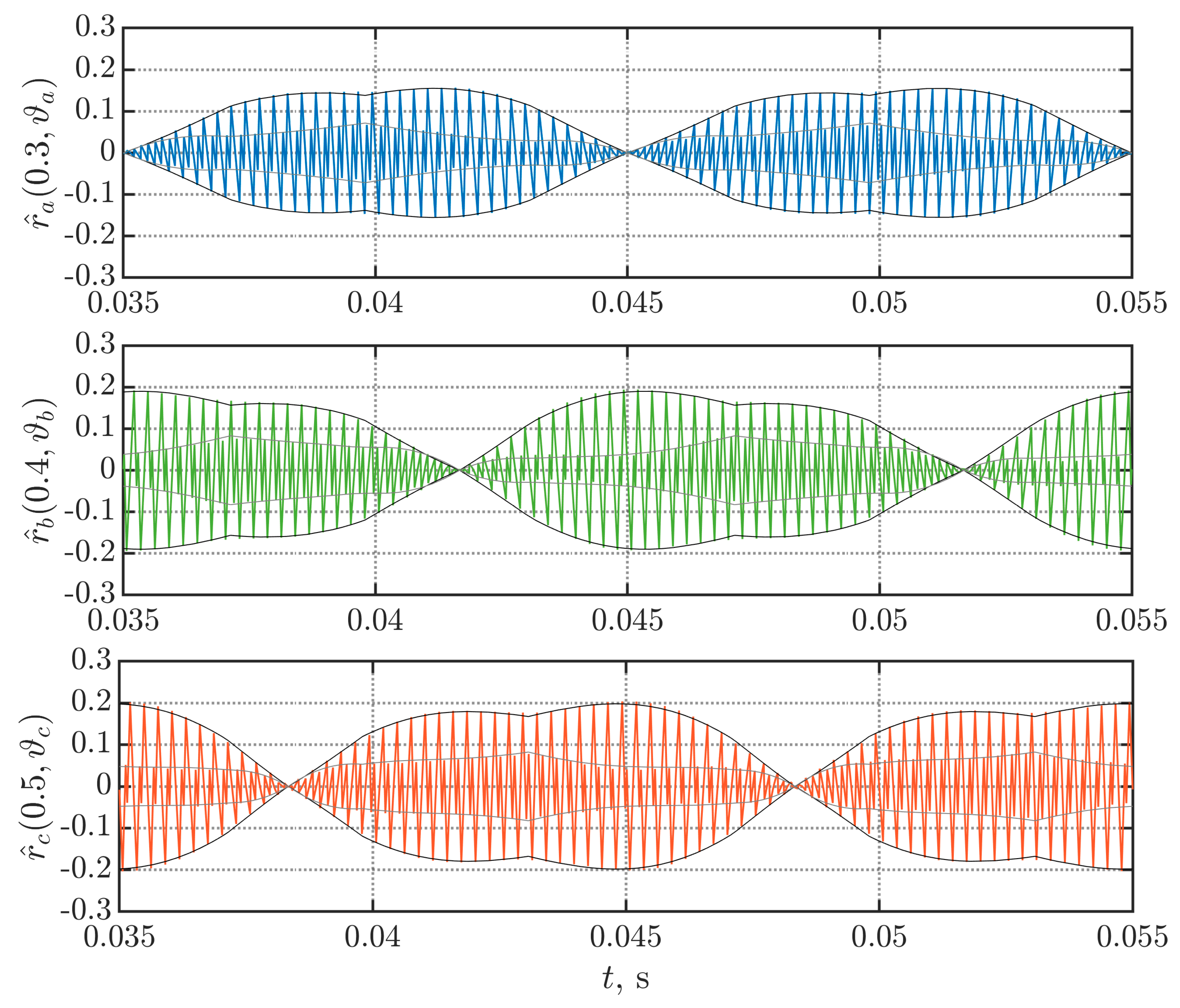
To prove the validity of Equations (18)–(21), Figure 4, Figure 5 and Figure 6 present simulation results for phase currents and normalized phase current ripples in the case of magnitude unbalance (ma = 0.3, mb = 0.4, mc = 0.5). The aforementioned set of modulation indices has been chosen arbitrarily, and it is used throughout the whole paper for the purpose of fair comparison. However, it should be pointed out that the derived equations are equally valid for any set of modulation indices within the modulation range. Simulation parameters are given in Table 1. As can be observed, the current ripple envelopes have properly bounded the actual values obtained by the simulation for both examined PWM strategies.
By considering positive and negative half-waves of the ripple envelope, the primary and secondary normalized peak-to-peak current ripples can be calculated as follows:
{ r ^ x , p p ( m x , ϑ x ) =   2 | r ^ x , p k ( m x , ϑ x ) | r ^ x , p p ( m x , ϑ x ) =   2 | r ^ x , p k ( m x , ϑ x ) |
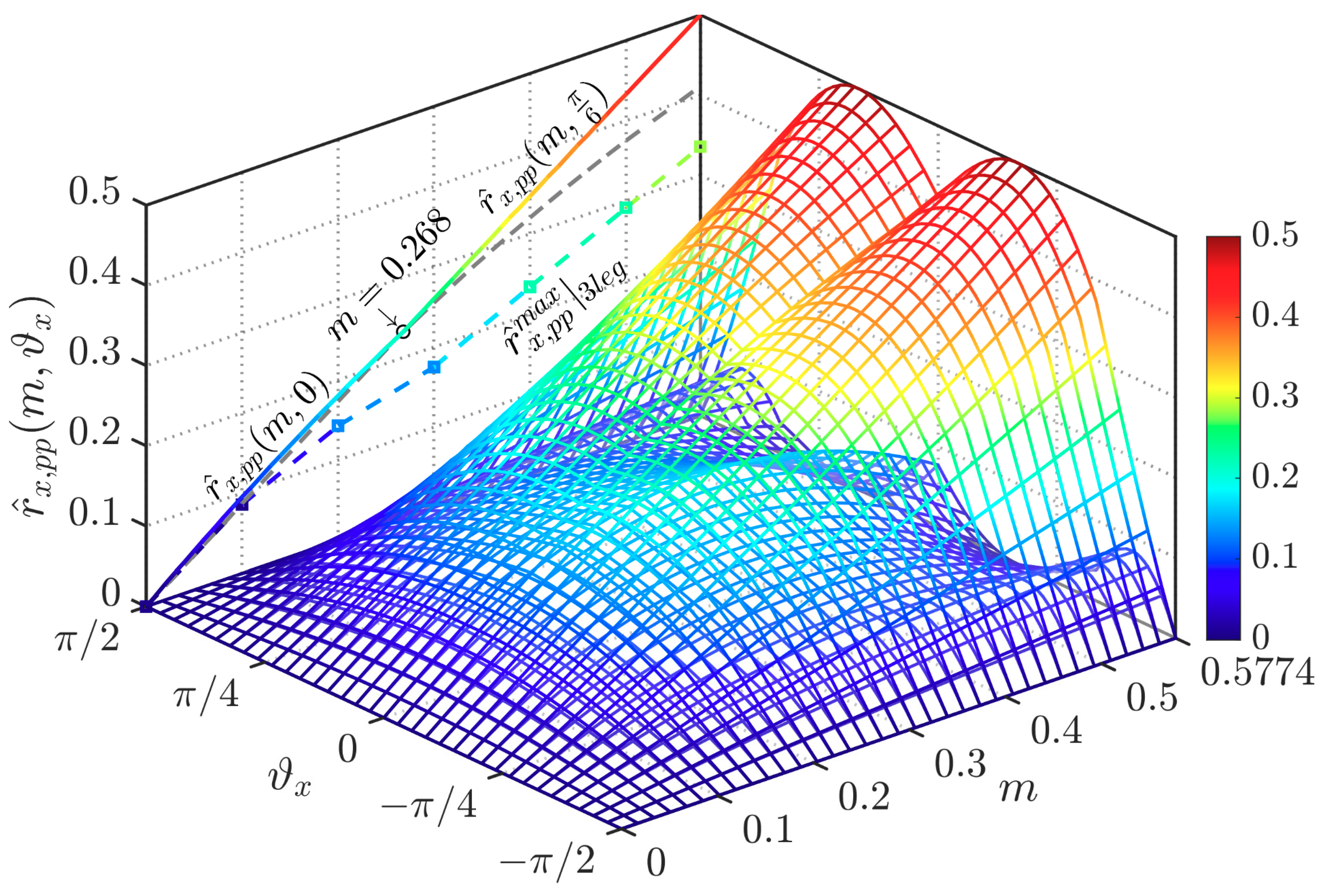
By introducing Equations (19)–(21) into Equation (22), the primary and secondary normalized peak-to-peak current ripples can be determined and depicted in Figure 7 and Figure 8 for SPWM and CPWM, respectively.
It should be noted that Equation (19) is valid under both balanced and unbalanced working conditions (Figure 7). However, Equations (20) and (21) are only valid under the balanced case (Figure 8).
In Figure 7, the colored solid-trace projection on the left-hand side plane represents the maximum of peak-to-peak current ripple in the whole range of modulation index for SPWM (occurs at ϑ = 0). However, the maximum of peak-to-peak current ripple has two local maxima within the range of modulation index in the case of CPWM, as shown in Figure 8 by the colored solid trace. It can be noted that the maxima occur at ϑ = 0 within m = [0, 2–√3] and at ϑ = π /6 for m = [2–√3, 1/√3]. The dashed gray line shows how those maxima functions propagate in the rest of the modulation range. As visible, the maximum of the peak-to-peak current ripple depends only on the primary peak-to-peak current ripple. Furthermore, both plots include the maximum peak-to-peak current ripples for the three-leg counterparts (colored dashed lines with markers), for the sake of comparison.

3.2. Phase Current Ripple RMS

The RMS of the phase current ripple can be effectively determined on the base of primary and secondary ripple envelopes Equations (14) and (15). In particular, with reference to the half switching period Tsw/2 (see Figure 2), the instantaneous current ripple can be expressed by the composition of its average (DC) and its alternate (AC) components:
i ^ x ( t ) = i ^ x d c ( t ) + i ^ x a c ( t )
The RMS value of the average component over the switching period corresponds to the average component itself, and it can be easily determined basing on the ripple envelopes as:
I ^ x d c ( t ) | T s w = i ^ x , p k ( t ) + i ^ x , p k ( t ) 2 = V d c 2 L f s w u x ( t ) u x ( t ) + 2   γ ( t ) 2
Since the alternate component consists of a triangular waveform ranging between the two evaluated extrema in Equations (14) and (15), its RMS on the switching period can be calculated by taking into account its crest factor √3 as:
I ^ x a c ( t ) | T s w = i ^ x , p k ( t ) i ^ x , p k ( t ) 2 3 = V d c 2 L f s w u x ( t ) 1 u x ( t ) 2 3
It should be noticed that the alternate component Equation (25) does not depend on the common-mode signal injection.
Given that DC and AC components are orthogonal, and due to the symmetry of the current ripple in the fundamental period, the total RMS of current ripple can be obtained by combining the current ripple RMS components Equations (24) and (25). By integrating over the phase angle interval [0, π/2], it leads to:
I ^ x = 2 π 0 π 2 { [ I ^ x d c ( ϑ ) | T s w ] 2 + [ I ^ x a c ( ϑ ) | T s w ] 2 } d ϑ
The RMS value of current ripple for SPWM can be found by introducing Equations (8), (24) and (25) into Equation (26) as:
I ^ x ( m x ) | S P W M = V d c 2 L f s w   m x 2 6 1 16 3 π m x + 3   m x 2
Similarly, considering Equation (9) and setting ma = mb = mc = m, the RMS in the case of balanced CPWM can be computed by:
I ^ x ( m ) | C P W M = V d c 2 L f s w   m 2 6 1 16 3 π m + ( 9 2 27 3 8 π ) m 2
Both Equations (27) and (28) can be normalized in similar way as Equation (18), giving:
R ^ x ( m x ) | S P W M = m x 2 6 1 16 3 π m x + 3   m x 2
R ^ x ( m ) | C P W M m 2 6 1 16 3 π m + 2.6   m 2
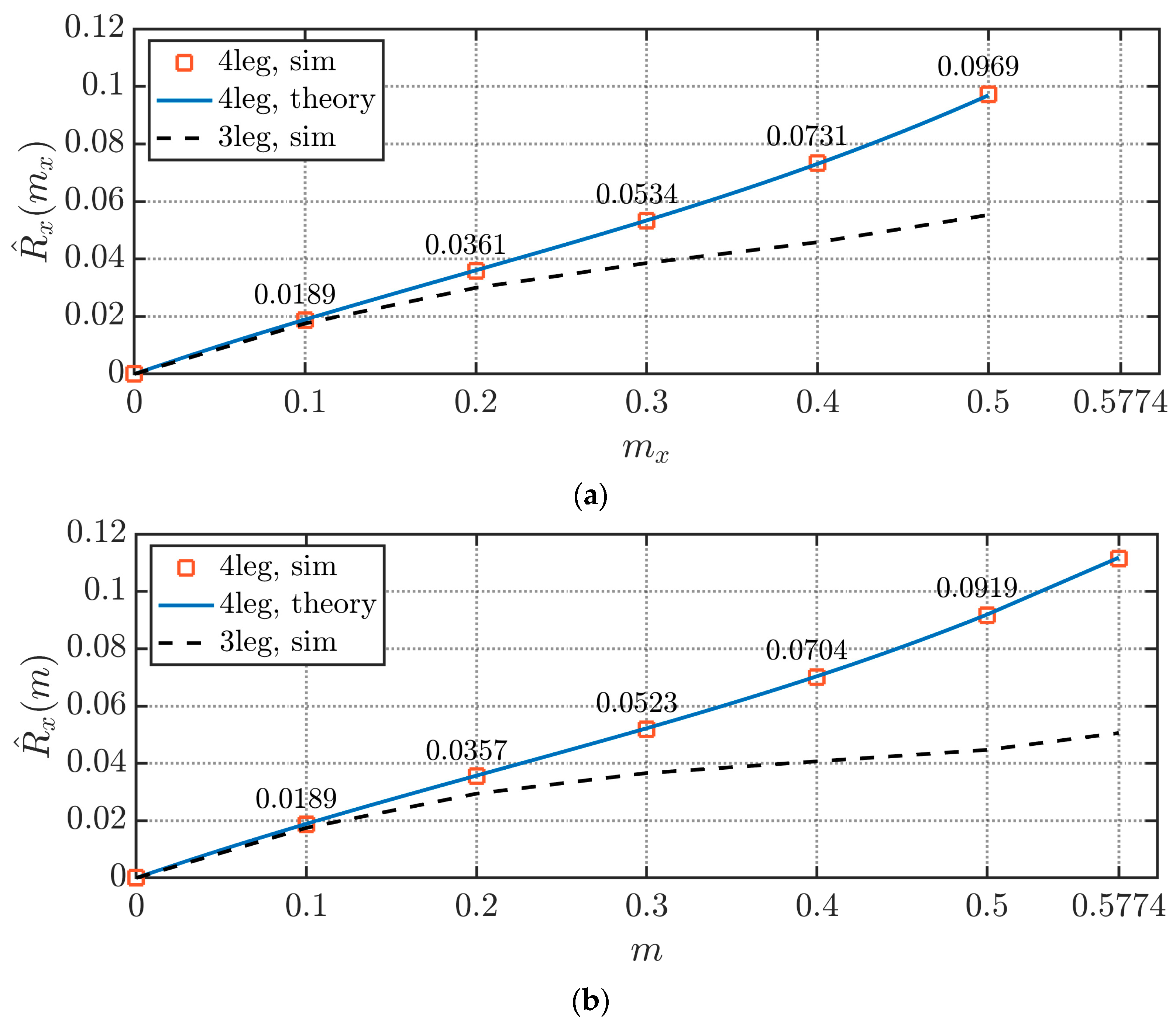
By comparing Equations (29) and (30), it is possible to conclude that CPWM has slightly lower RMS current ripple with regard to SPWM, in the whole modulating index range (the coefficient of m2 in Equation (30) is 2.6 in comparison with 3.0 in Equation (29). This slightly superior performance is more noticeable for high values of mx as shown in Figure 9.
Figure 9 shows a good matching between the normalized current ripple RMS calculated by Equations (29) and (30) and the corresponding values obtained by simulations respectively for SPWM (Figure 9a) and CPWM (Figure 9b). In addition, Figure 9 also illustrates a comparison of the normalized current ripple RMS as a function of modulation index between four- and three-leg three-phase (dashed line) VSCs. In the legend of these plots, “4leg” stands for four-leg converter configuration, while “3leg” stands for its three-legged counterpart (three-leg VSC), employing the two modulating schemes described above (SPWM and CPWM). It should be noted that, for each phase, the current ripple RMS is almost the same for the four-leg VSC with respect to the three-leg VSC within low-value modulation indices (m < 0.1), but it becomes almost the double for high modulation indices. As expected, in terms of phase currents ripple, there is an evident drawback when employing the four-leg converter instead of the three-leg converter in the case of balanced working conditions. Therefore, in this case, the 4th leg should be disabled to achieve three-leg three wires operations, with reduced phase currents ripple.
Viatkin et al. have proposed a current ripple RMS approximated formulation (in the case of SPWM only) based on the sole primary ripple envelope [23]. Although this practice provides simpler formulations, it gives place to an inevitable current ripple RMS overestimation. This is due to approximating the piecewise current ripple waveform with a triangular waveform without considering the contribution attributable to the secondary ripple envelope as performed in the previous developments.

4. Analysis of Neutral Current Ripple

4.1. Neutral Current Ripple Waveform

The total current in the neutral wire is simply obtained by adding the three phase currents. The fundamental current component in the neutral is zero when modulation/load is balanced, while it differs from zero in case of unbalanced modulation/load. Independently from the presence of the fundamental component, the current ripple component is circulating in the neutral wire, despite the balanced or unbalanced modulation/load. As it was previously discussed in Section 2.2, Figure 2 evidently demonstrates that the primary peaks of the phase current ripples always take place concurrently, i.e., at the commutation instant of the 4th leg, regardless of phase modulating signals ux. Thus, the primary peaks of phase current ripples overlap each other. Taking into consideration this fact, and applying Kirchhoff’s law, the envelope of normalized current ripple in the neutral wire can be simply found as:
r ^ n , p k = x = a , b , c r ^ x , p k ( m x , ϑ x )
By introducing Equation (18) into (31) and considering that, due to the current ripple envelope symmetry, the peak-to-peak value of the ripple can be found as the double of its absolute peak value, it gives:
r ^ n , p p = | u a ( t ) | + | u b ( t ) | + | u c ( t ) | + γ ( t ) [ u a ( t ) + u b ( t ) + u c ( t ) ]
In balanced, three-phase systems (ma = mb = mc = m) with generic common-mode injection γ(t), the second term of the right-hand side becomes zero, simplifying Equation (32) as:
r ^ n , p p = | u a ( t ) | + | u b ( t ) | + | u c ( t ) |
It should be highlighted that in Equation (33), the peak-to-peak neutral current ripple becomes independent on the common mode injection γ(t); therefore, the same equation is valid for both considered modulations strategies (SPWM and CPWM) for a balanced system. In case of SPWM, Equation (33) is still valid, even under unbalanced operations, because γ(t) = 0.
In order to check the accuracy of Equations (32) and (33), Figure 10 and Figure 11 present the results of numerical simulations for the neutral current. Figure 10 depicts the neutral currents (brown traces) along with their primary envelopes (black traces) for SPWM (Figure 10a) and CPWM (Figure 10b) under magnitude unbalance (ma = 0.3, mb = 0.4, mc = 0.5). Correspondingly, Figure 11 shows the normalized peak neutral current ripples with the envelopes. Simulations have been performed on the basis of the system parameters given in Table 1.
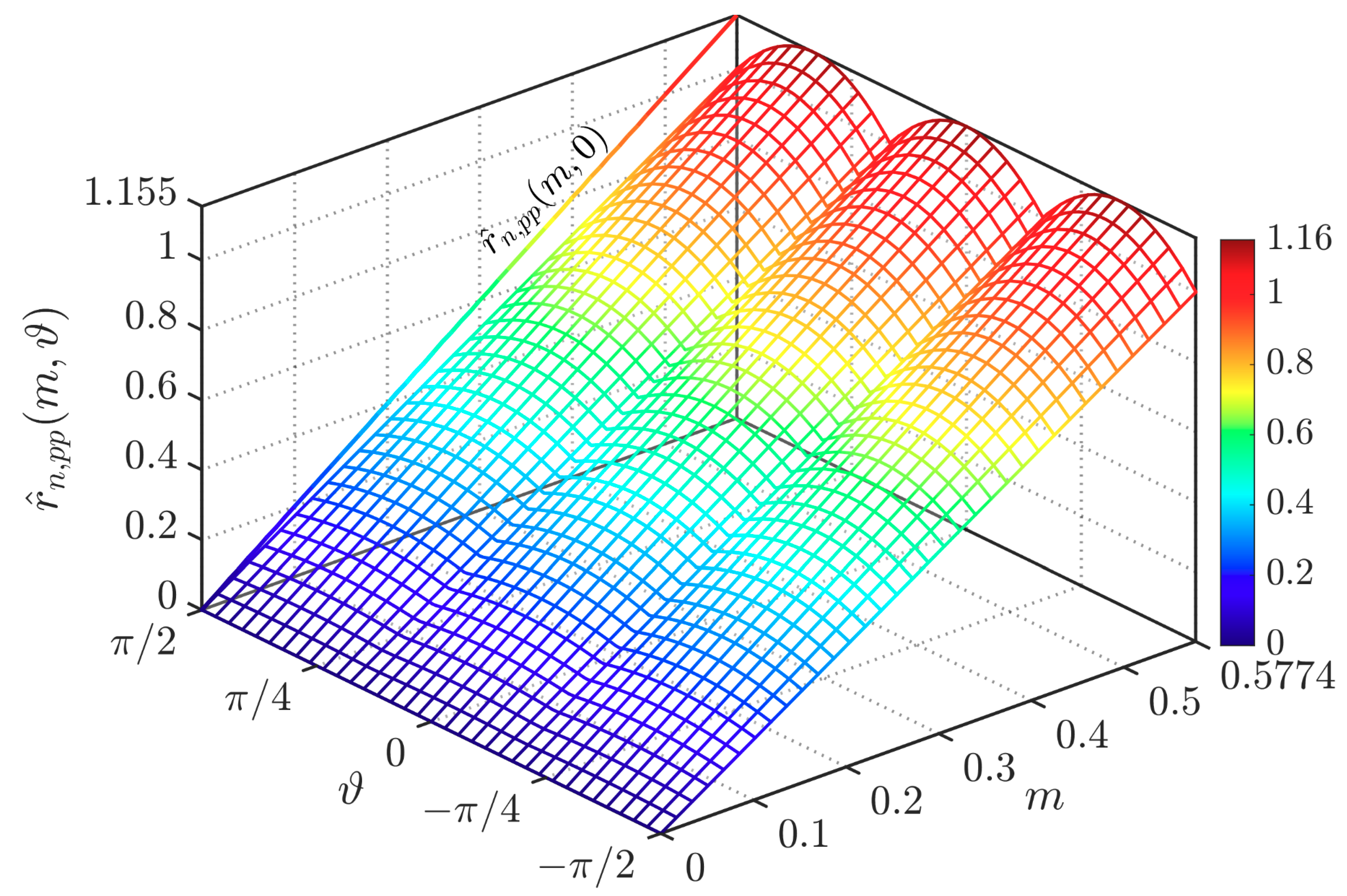
Figure 12 presents the normalized peak-to-peak neutral ripple in balanced working condition, for both SPWM and CPWM, within modulation ranges [0, 0.5] and [0, 1/√3], respectively. The maximum of normalized peak-to-peak neutral current ripple, represented by a colored solid projection on the left-hand side plane, can be found at phase angle ϑ = 0 ± hπ/3, where h is an integer number.

4.2. Neutral Current Ripple RMS

As mentioned in Section 2, due to the fact that the neutral current depends on the phase variables (ma, mb, mc, φa, φb, and φc), a generic analytical evaluation of the current ripple RMS, for all possible unbalanced cases, is cumbersome. Furthermore, for the most grid-tied applications, calculations under unbalanced modulation do not have practical use because general converter voltage unbalances are often in the order of a few percent for both magnitude and phase. Therefore, the findings of this subsection refer to balanced case (ma = mb = mc = m) only. In this case, three time slots for the neutral current ripple can be introduced, as shown in Figure 13:
{ t n 1 = T s w 2 ( u a * ( t ) u n ( t ) ) = T s w 2 u a ( t ) t n 2 = T s w 2 ( u n ( t ) u b * ( t ) ) = T s w 2 u b ( t ) t n 3 = T s w 2 ( u b * ( t ) u c * ( t ) ) = T s w 2 ( u b ( t ) u c ( t ) )
Because γ(t) does not appear in Equation (34), the following analysis is valid for any type of common-mode injection.
The voltage v ^ n depicted in Figure 13 has more than two levels. Consequently, it is not possible to extrapolate neutral current ripple în as a single triangular waveform. For this reason, the calculation of its RMS cannot be as straight as for the phase current ripple. On the other hand, în profile has a linear piecewise shape, having three distinctive intervals in each half of a switching period. The current ripple in these intervals has a sawtooth-like waveform. Therefore, it can be examined within each interval separately, adopting the same approach already introduced for the phase ripple RMS. The RMS value of neutral current ripple Înk over each k-th interval can be written as:
I ^ n ( t ) | k = [ I ^ n d c ( t ) | k ] 2 + [ I ^ n a c ( t ) | k ] 2
According to Figure 13, Equation (35) can be explicitly written as:
I ^ n ( t ) | k = { I ^ n ( t ) | 1 = V d c L ( t n 1 2 ) 2 + ( t n 1 2 3 ) 2 I ^ n ( t ) | 2 = V d c L ( t n 1 t n 2 ) 2 + ( t n 2 2 3 ) 2 I ^ n ( t ) | 3 = V d c L ( t n 3 2 ) 2 + ( t n 3 2 3 ) 2
Thanks to the half-wave symmetry of the neutral current ripple within the switching period Tsw, its RMS can be computed basing on Equation (36) as:
I ^ n ( t ) | T s w = 2 T s w k = 1 3 t n k [ I ^ n ( t ) | k ] 2
Finally, taking advantage of the neutral ripple current symmetry (in balanced cases only), the total neutral ripple RMS is obtained by integrating Equation (37) as:
I ^ n ( m ) = 6 π 0 π 6 [ I ^ n ( ϑ ) | T s w ] 2 d ϑ = V d c 2 L f s w m 3 2 3 2 π
Similarly to previous developments, the normalization of Equation (38) leads to:
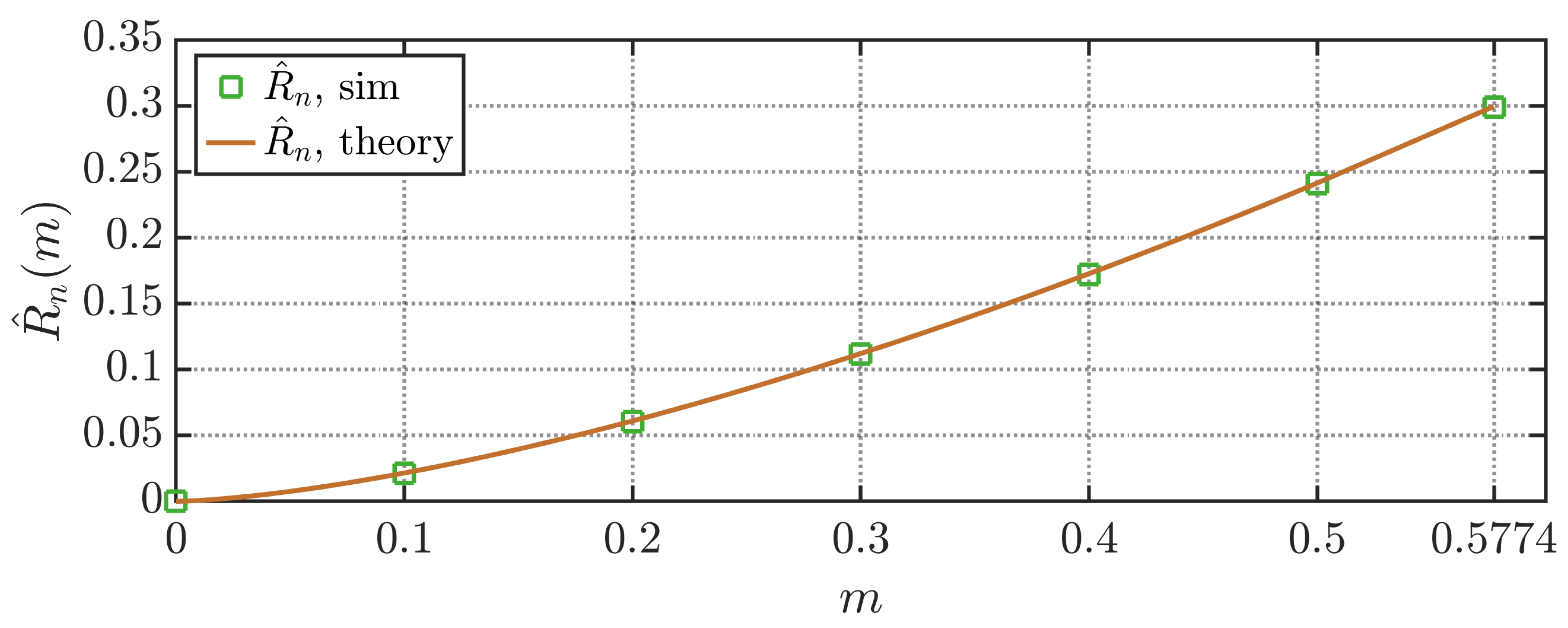
R ^ n ( m ) = m 3 2 3 2 π
Figure 14 illustrates simulation results of the neutral current RMS for several modulation indices (green squares) and its analytical evaluation (brown trace) given by Equation (39). A good match can be observed among them.

5. Experimental Results

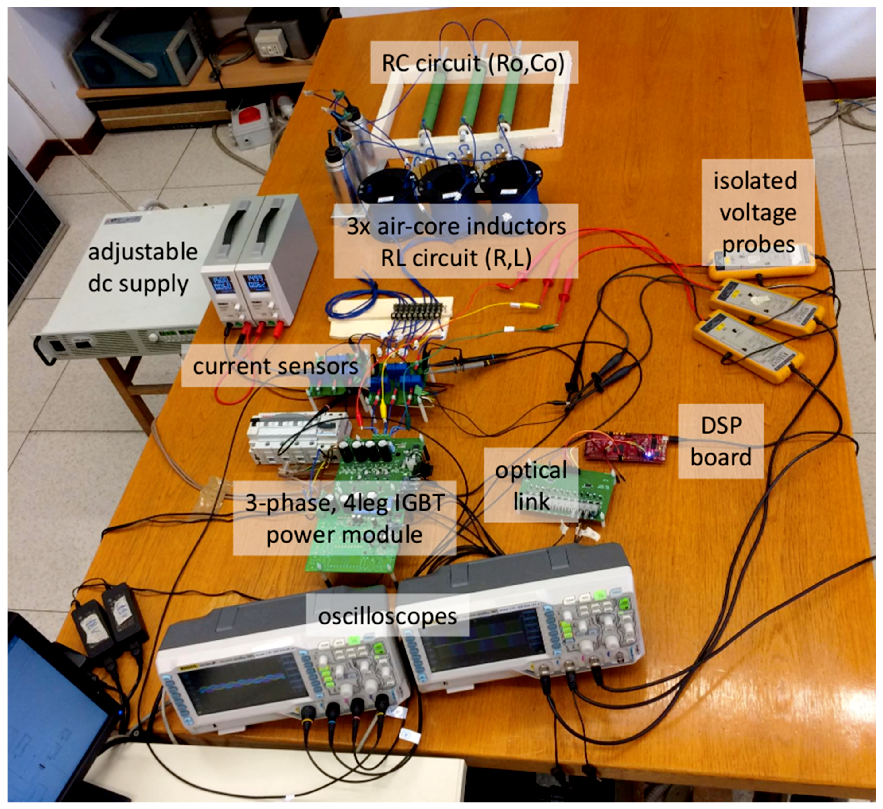
Theoretical findings have been verified by experimental tests carried out with the setup shown in Figure 15, considering the same circuit configuration depicted in Figure 3. The main parts of the setup consist of an adjustable DC supply (GEN100-33, TDK- Lambda), a four-leg VSC, formed by two IGBT-based power modules (PS22A76, Mitsubishi Electric), three air-core inductors, representing series RL circuit, three parallel RC circuits, composed by the parallel connection of an AC-link capacitor and a resistor per each phase, current sensors (LA 55-P, LEM), isolated differential voltage probes (TA057, Pico), and DSP microcontroller board (TMS320 F28379D, Texas Instruments). The main setup parameters are given in Table 1.
The converter’s AC side is linked with the combined RLC circuit having unity power factor at 50 Hz and emulating a grid connection. The power module is driven by the DSP board via intermediate optical links. The modulating signals for the PWM technique are generated by DSP board, controlled in real-time by MATLAB/Simulink.
The measured currents and voltages were initially acquired and processed as a set of sampled datapoints via two digital oscilloscopes (DS1054Z, Rigol). The sampling frequency for all scope channels has been fixed at 5 MHz. The results visualization was accomplished via MATLAB. No signal’s filtering has been applied.
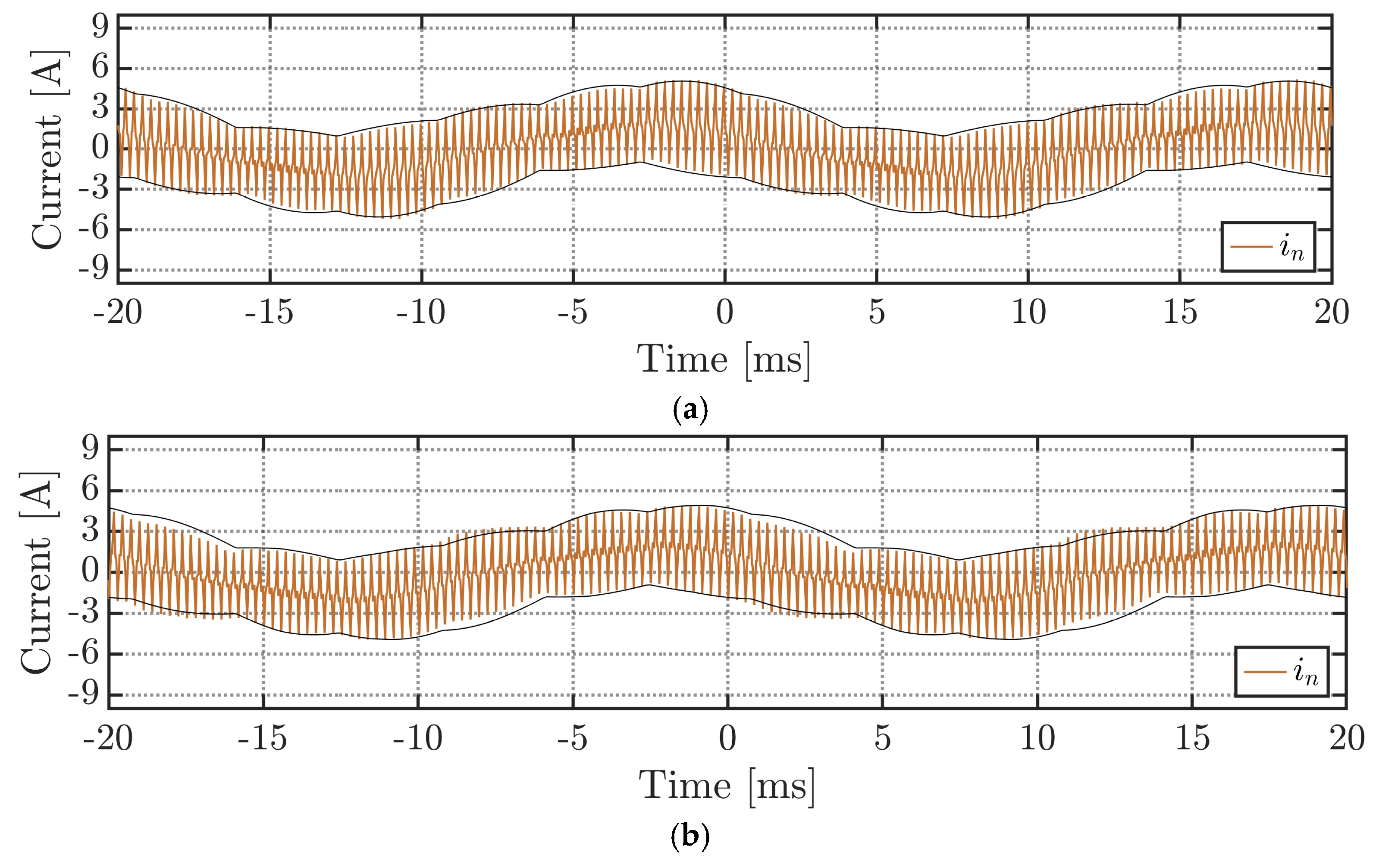
Figure 16 depicts measured phase currents with their analytical primary (black) and secondary (gray) envelopes for the previously simulated case study (modulation index unbalance ma = 0.3, mb = 0.4, and mc = 0.5), which has been analyzed in Section 3 (reference to Figure 4). The instantaneous neutral currents for sinusoidal PWM (Figure 17a) and centered PWM (Figure 17b), along with their envelopes, are shown in Figure 17.
Figure 18 displays RMS values of the phase and neutral switching current ripples for both modulation methods. The first thing that must be noted is a good correlation between analytically calculated Equations (27), (28) and (38) and experimentally obtained values at specific moduation indices. Furthermore, in Figure 18 one may notice that experimentally acquired RMS values of the neutral current ripple for CPWM overlap the corresponding counterparts from SPWM. Finally, a modest improvement of RMS phase current ripple can be seen in case of CPWM for upper modulation region [0.3, 0.5] in comparison with SPWM.

6. Discussion

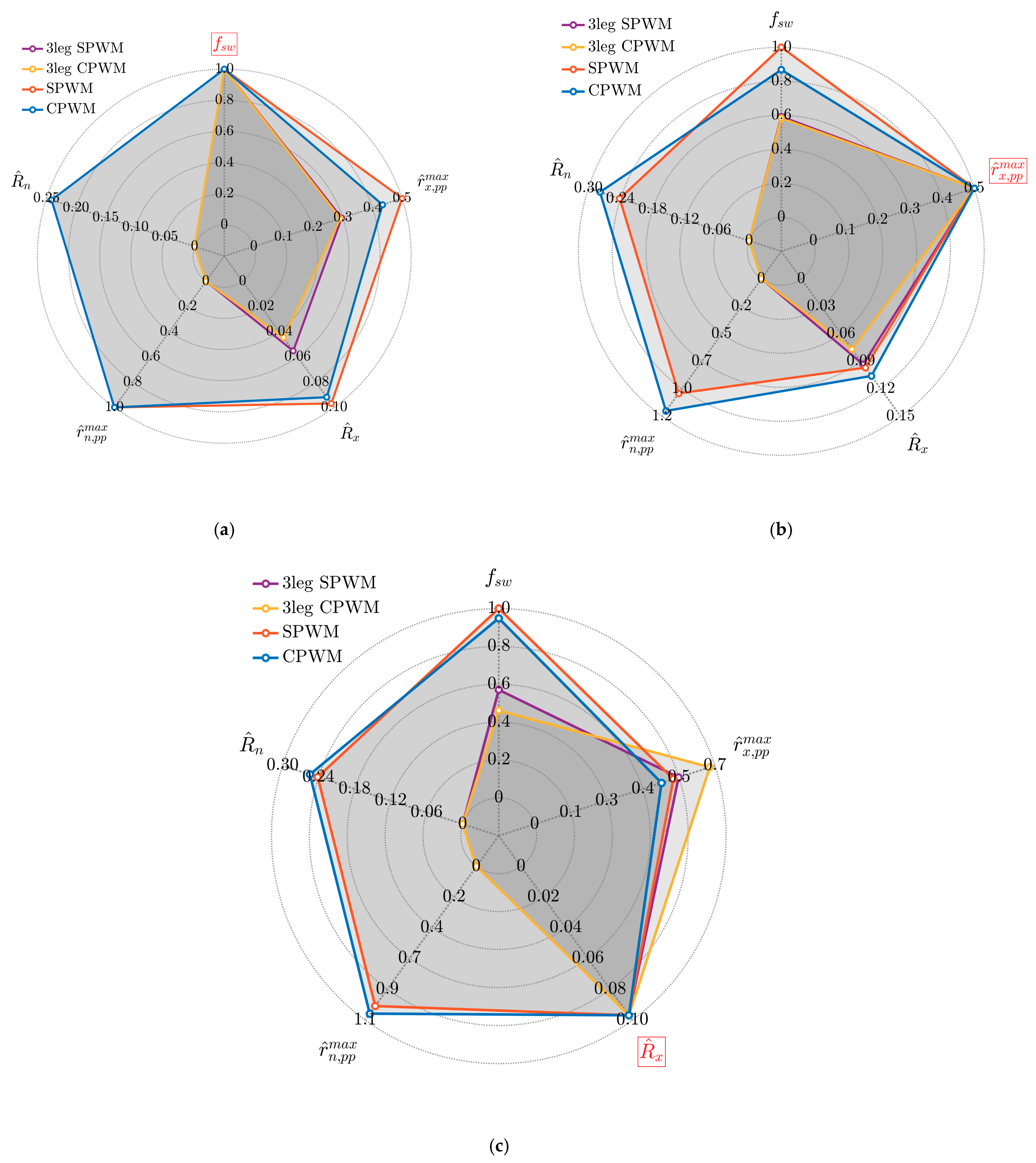
The findings presented above demonstrate, in a rather scattered way, the differences in AC-current-ripple-related performance between a typical three-leg voltage source converter and its four-leg counterpart. Figure 19 summarizes the properties of the AC current ripple and gives a little more insight about how these characteristics correlate with each other. In the legend of these subplots, “3leg” stands for a three-leg VSC that employs two modulating schemes, namely SPWM and CPWM (SVM). Similarly, the other two traces represent characteristics for a four-leg voltage source converter (by default the abbreviation “4leg” was omitted for shorter notation) also in the case of examined modulation strategies (SPWM and CPWM). In this case, the considered VSC topologies and modulation techniques are compared in terms of five characteristics, namely switching frequency, maximum normalized peak-to-peak values of phase and neutral switching current ripples, and normalized RMS values of phase and neutral switching current ripples. As it was shown above, peak-to-peak and RMS values of AC current ripple are inversely proportional to switching frequency, thus, it is possible to derive their formulation as a function of switching frequency. In this instance, by varying switching frequency, it is possible to fix AC current ripple properties at a certain level among compared topologies/modulation strategies to highlight their capabilities. For fair comparison, the operating point was chosen at m = 0.5 (balanced case) because this modulation index is common for both of the compared modulations, although CPWM in this sense has an additional advantage of an increased modulation range. In addition, Figure 19 presents only three subcases with either fixed switching frequency, maximum normalized peak-to-peak value of phase current ripple, or normalized RMS value of phase current ripple. That has been made mainly because the characteristics of neutral current ripple are independent from the common mode injection introduced into a modulating signal, as long as the modulation is balanced and due to the fact that, in a three-leg VSC, these values are zero, given that the neutral wire missing.
Figure 19a illustrates the measures at the fixed, identical switching frequency, which is exactly the case presented above. It is quite evident from this subplot that while operating in a balanced three-phase mode, the 4th leg of a four-leg VSC should be disconnected from the rest of the circuit because it causes not only additive power losses in the neutral wire but also excessive losses and an overall worsened harmonic pollution in the phases. Another interesting point that draws attention is that unlike the difference in phase current ripple characteristics between SPWM and CPWM in case of a three-leg VSC, this variance has quite opposite behavior. In other words, passing from operation with SPWM to CPWM, the peak-to-peak value of phase current ripple will be reduced greater in comparison to its associated RMS value.
By fixing the values of maximum normalized peak-to-peak phase current ripple and its RMS counterpart at their common maximum levels, the subplots given in Figure 19b,c can be obtained. It is interesting to notice that, having the same peak-to-peak values of phase current ripple in both modulation cases (SPWM and CPWM) for a four-leg VSC, the switching frequency in the CPWM case can be cut down by 13.25%. On the other hand, having fixed their RMS values at the same level, this switching frequency reduction is just 5.14%. Making a similar comparison between the three-leg and the four-leg topologies, a significant lessening of switching frequency can be achieved. For instance, in the case of identical peak-to-peak values of phase current ripple, this reduction could attain 40.8% for SPWM and 28.5% for CPWM. Likewise, with a matching RMS value of phase current ripple, switching frequency can be decreased by 42.9% for SPWM and 48.7% for CPWM. In addition, because peak-to-peak and RMS values of AC current ripple have the same dependency from both the phase inductance value and the switching frequency, the same percentage reduction on the inductance can be seen if the inductance value is considered instead of the switching frequency.
Overall, it was shown that the behavior and efficiency of a four-leg VSC can be optimized not only by selecting the most favorable modulation strategy but also by disconnecting the 4th (neutral) leg in balanced three-phase operational mode if the specific application permits to do so.

7. Conclusions

This paper provided a detailed analysis of the main characteristics of the AC current switching ripple for a three-phase, four-leg voltage source converter. This configuration that can be used as the front-end stage of an OBCs in order to get bidirectional power flow (G2V and V2G) and unbalanced charging or discharging grid currents to balance local loads. In particular, the peak-to-peak current ripple has been analytically derived in the whole fundamental period as a function of modulating signals for a generic carrier-based PWM technique.
The analysis has been focused to sinusoidal PWM and centered PWM, obtaining expressions for the peak-to-peak current ripples as a function of modulation index and phase angle. In addition, based on the evaluated peak-to-peak value, the current ripple RMS has been determined as well. The achieved mathematical formulation covers both phase and neutral currents under balanced and unbalanced working conditions. The RMS values of phase and neutral current ripples, given by derived equations along with results from numerical simulations, have been compared for CPWM and SPWM. This comparison, firstly, validates high precision and applicability of the obtained theoretical expressions and, secondly, illustrates a slight advantage of CPWM over SPWM in terms of AC current ripple in three-phase four-leg VSCs. It has also been proven that the common mode injection of the CPWM does not affect the neutral current envelop with respect to the SPWM. Moreover, a comparison with similar characteristics of the three-phase three-leg VSC has been provided as a reference. The significant advantage of three-leg VSCs usage in balanced working conditions over their four-leg counterparts has been demonstrated. Experimental results have been provided to validate the derived AC current ripple equations, with very good accuracy.
The proposed equations and diagrams can be successfully adopted to design the four-leg AC/DC converter basing on the grid codes. In particular, given the current ripple and/or the current THD/TDD restrictions, the AC-link inductors can be properly sized, and the proper switching frequency can be established for the given operating conditions.

Author Contributions

Conceptualization, A.V., R.M., M.H., M.R. and G.G.; methodology, A.V., R.M., M.H., M.R. and G.G.; software, A.V. and R.M.; validation, A.V., R.M. and M.H.; formal analysis, A.V., R.M., M.H. and G.G.; investigation, A.V., R.M. and M.H.; resources, A.V., R.M. and M.H.; data curation, A.V. and R.M.; writing—original draft preparation, A.V., R.M. and M.H.; writing—review and editing, A.V., R.M., M.H., M.R. and G.G.; visualization, A.V. and R.M.; supervision, M.R. and G.G. All authors have read and agreed to the published version of the manuscript.

Funding

This research received no external funding.

Institutional Review Board Statement

Not applicable.

Informed Consent Statement

Not applicable.

Data Availability Statement

Data presented in this study are available in the article.

Conflicts of Interest

The authors declare no conflict of interest.

Nomenclature

xIndex for phases a, b, c, and neutral n, used as a subscript
v x , i x Converter’s instantaneous voltage and current
v ¯ x , i ¯ x Low-frequency components of instantaneous voltage and current (averaged over the switching period)
v ^ x , i ^ x High-frequency (switching frequency) ripple components of instantaneous voltage and current
u x * Modulating signals
γCommon-mode injection
mxModulation index (normalized by dc-link voltage Vdc)
ϑxPhase power angle
i ^ x , p k , i ^ x , p p Primary peak (pk) and primary peak-to-peak (pp) current ripple wrapping envelopes
r ^ x , p k , r ^ x , p p Normalized primary peak (pk) and primary peak-to-peak (pp) current ripple wrapping envelopes
i ^ x , p k , i ^ x , p p Secondary peak (pk) and secondary peak-to-peak (pp) current ripple wrapping envelopes
r ^ x , p k , r ^ x , p p Normalized secondary peak (pk) and secondary peak-to-peak (pp) current ripple wrapping envelopes
I ^ x Total current ripple RMS
R ^ x Normalized total current ripple RMS

References

  1. De Freitas Takami, M.H.; da Silva, S.A.O.; Sampaio, L.P. Dynamic performance comparison involving grid-connected PV systems operating with active power-line conditioning and subjected to sudden solar irradiation changes. IET Renew. Power Gener. 2019, 13, 587–597. [Google Scholar] [CrossRef]
  2. Carrasco, G.; Silva, C.A.; Pena, R.; Cardenas, R. Control of a Four-Leg Converter for the Operation of a DFIG Feeding Stand-Alone Unbalanced Loads. IEEE Trans. Ind. Electron. 2015, 62, 4630–4640. [Google Scholar] [CrossRef]
  3. Khadkikar, V.; Chandra, A.; Singh, B. Digital signal processor implementation and performance evaluation of split capacitor, four-leg and three H-bridge-based three-phase four-wire shunt active filters. IET Power Electron. 2011, 4, 463–470. [Google Scholar] [CrossRef]
  4. Yaramasu, V.; Rivera, M.; Wu, B.; Rodriguez, J. Model Predictive Current Control of Two-Level Four-Leg Inverters—Part I: Concept, Algorithm, and Simulation Analysis. IEEE Trans. Power Electron. 2013, 28, 3459–3468. [Google Scholar] [CrossRef]
  5. Li, A.; Jiang, D.; Kong, W.; Qu, R. Four-Leg Converter for Reluctance Machine With DC-Biased Sinusoidal Winding Current. IEEE Trans. Power Electron. 2019, 34, 4569–4580. [Google Scholar] [CrossRef]
  6. Viatkin, A.; Hammami, M.; Grandi, G.; Ricco, M. Analysis of a Three-Phase Four-Leg Front-End Converter for EV Chargers with Balanced and Unbalanced Grid Currents. In Proceedings of the IECON 2019—45th Annual Conference of the IEEE Industrial Electronics Society, Lisbon, Portugal, 14–17 October 2019; pp. 3442–3449. [Google Scholar]
  7. Fu, Y.; Li, Y.; Huang, Y.; Lu, X.; Zou, K.; Chen, C.; Bai, H. Imbalanced Load Regulation Based on Virtual Resistance of A Three-Phase Four-Wire Inverter for EV Vehicle-to-Home Applications. IEEE Trans. Transp. Electrif. 2019, 5, 162–173. [Google Scholar] [CrossRef]
  8. Lin, Z.; Ruan, X.; Jia, L.; Zhao, W.; Liu, H.; Rao, P. Optimized Design of the Neutral Inductor and Filter Inductors in Three-Phase Four-Wire Inverter with Split DC-Link Capacitors. IEEE Trans. Power Electron. 2019, 34, 247–262. [Google Scholar] [CrossRef]
  9. Hammami, M.; Ricco, M.; Viatkin, A.; Mandrioli, R.; Grandi, G. Evaluation of AC Current Ripple in case of Split-Capacitor Three-Phase Four Wires Inverters. In Proceedings of the 2020 6th IEEE International Energy Conference (ENERGYCon), Gammarth, Tunisia, 28 September–1 October 2020; pp. 128–132. [Google Scholar]
  10. Hammami, M.; Mandrioli, R.; Viatkin, A.; Ricco, M.; Grandi, G. Analysis of Input Voltage Switching Ripple in Three-Phase Four-Wire Split Capacitor PWM Inverters. Energies 2020, 13, 5076. [Google Scholar] [CrossRef]
  11. Hintz, A.; Prasanna, R.; Rajashekara, K. Comparative Study of Three-phase Grid Connected Inverter Sharing Unbalanced Three-phase and/or Single-phase systems. In Proceedings of the 2015 IEEE Energy Conversion Congress and Exposition (ECCE), Montreal, QC, Canada, 20–24 September 2015; pp. 6491–6496. [Google Scholar]
  12. Zhao, W.; Ruan, X.; Yang, D.; Chen, X.; Jia, L. Neutral Point Voltage Ripple Suppression for a Three-Phase Four-Wire Inverter with an Independently Controlled Neutral Module. IEEE Trans. Ind. Electron. 2017, 64, 2608–2619. [Google Scholar] [CrossRef]
  13. Fu, Y.; Li, Y.; Huang, Y.; Bai, H.; Zou, K.; Lu, X.; Chen, C. Design Methodology of a Three-Phase Four-Wire EV Charger Operated at the Autonomous Mode. IEEE Trans. Transp. Electrif. 2019, 5, 1169–1181. [Google Scholar] [CrossRef]
  14. Wong, M.C.; Zhao, Z.Y.; Han, Y.D.; Zhao, L.B. Three-dimensional pulse-width modulation technique in three-level power inverters for three-phase four-wired system. IEEE Trans. Power Electron. 2011, 16, 418–427. [Google Scholar] [CrossRef] [Green Version]
  15. Golwala, H.; Chudamani, R. New Three-Dimensional Space Vector-Based Switching Signal Generation Technique without Null Vectors and with Reduced Switching Losses for a Grid-Connected Four-Leg Inverter. IEEE Trans. Power Electron. 2016, 31, 1026–1035. [Google Scholar] [CrossRef]
  16. Kim, J.H.; Sul, S.K. A Carrier-Based PWM Method for Three-Phase Four-Leg Voltage Source Converters. IEEE Trans. Power Electron. 2004, 19, 66–75. [Google Scholar] [CrossRef]
  17. Hava, A.M.; Kerkman, R.J.; Lipo, T.A. Carrier-based PWM-VSI overmodulation strategies: Analysis, comparison, and design. IEEE Trans. Power Electron. 1998, 13, 674–689. [Google Scholar] [CrossRef] [Green Version]
  18. Grandi, G.; Loncarski, J. Evaluation of current ripple amplitude in three-phase PWM voltage source inverters. In Proceedings of the 2013 International Conference-Workshop Compatibility and Power Electronics, Ljubljana, Slovenia, 5–7 June 2013; pp. 156–161. [Google Scholar]
  19. Grandi, G.; Loncarski, J.; Dordevic, O. Analysis and Comparison of Peak-to-Peak Current Ripple in Two-Level and Multilevel PWM Inverters. IEEE Trans. Ind. Electron. 2015, 62, 2721–2730. [Google Scholar] [CrossRef]
  20. Jiang, D.; Wang, F. Study of analytical current ripple of three-phase PWM converter. In Proceedings of the 2012 Twenty-Seventh Annual IEEE Applied Power Electronics Conference and Exposition (APEC), Orlando, FL, USA, 5–9 February 2020; pp. 1568–1575. [Google Scholar]
  21. Grandi, G.; Loncarski, J.; Seebacher, R. Effects of current ripple on dead-time distortion in three-phase voltage source inverters. In Proceedings of the 2012 IEEE International Energy Conference and Exhibition (ENERGYCON), Florence, Italy, 9–12 September 2012; pp. 207–212. [Google Scholar]
  22. Cai, W.; Shen, Y.; Xiao, X.; Wang, W.; Zhang, W.; Li, K.; Zhang, C.; Zhao, Z. Design of the Neutral Line Inductor for Three-phase Four-leg Inverters. In Proceedings of the 2019 IEEE Sustainable Power and Energy Conference (iSPEC), Beijing, China, 21–23 November 2019; pp. 2455–2460. [Google Scholar]
  23. Viatkin, A.; Mandrioli, R.; Hammami, M.; Ricco, M.; Grandi, G. Theoretical Analysis of the AC Current Ripple in Three-Phase Four-Leg Sinusoidal PWM Inverters. In Proceedings of the 2020 IEEE 29th International Symposium on Industrial Electronics (ISIE), Delft, Netherlands, 17–19 June 2020; pp. 796–801. [Google Scholar]
  24. Bouarfa, A.; Bodson, M.; Fadel, M. An optimization formulation of converter control and its general solution for the four-leg Two-level inverter. IEEE Trans. Control. Syst. Technol. 2018, 26, 1901–1908. [Google Scholar] [CrossRef]
  25. Hou, C.; Wang, P.; Chen, C.; Chang, C. Common Mode Voltage Reduction in Four-Leg Inverter with Multicarrier PWM Scheme. In Proceedings of the 2019 10th International Conference on Power Electronics and ECCE Asia (ICPE 2019—ECCE Asia), Busan, Korea, 27–30 May 2019; pp. 3223–3228. [Google Scholar]
  26. Mandrioli, R.; Viatkin, A.; Hammami, M.; Ricco, M.; Grandi, G. A Comprehensive AC Current Ripple Analysis and Performance Enhancement via Discontinuous PWM in Three-Phase Four-Leg Grid-Connected Inverters. Energies 2020, 13, 4352. [Google Scholar] [CrossRef]
Figure 1. On-board charger with a four-leg three-phase front-end converter.
Electronics 10 00116 g001
Figure 2. Modulating signals of corresponding legs in four-leg VSC (top), AC terminal voltage (middle), and phase A current (bottom) in one switching period in the case of a generic pulse-width modulation (PWM) pattern.
Electronics 10 00116 g002
Figure 3. Circuit scheme of a four-leg, three-phase VSC supplying unity power factor load emulating the AC grid (AC-link inductors are independent).
Electronics 10 00116 g003
Figure 4. Phase currents in the case of modulation index unbalance (ma = 0.3, mb = 0.4, mc = 0.5) with primary (black) and secondary (gray) current ripple envelopes for sinusoidal PWM (a) and centered PWM (b).
Electronics 10 00116 g004
Figure 5. Normalized phase current ripples in case of modulation index unbalance (ma = 0.3, mb = 0.4, mc = 0.5) with primary (black) and secondary (gray) envelopes for sinusoidal PWM.
Electronics 10 00116 g005
Figure 6. Normalized phase current ripples in case of modulation index unbalance (ma = 0.3, mb = 0.4, mc = 0.5) with primary (black) and secondary (gray) envelopes for centered PWM.
Electronics 10 00116 g006
Figure 7. Normalized primary (upper) and secondary (lower) peak-to-peak phase current ripples in case of SPWM.
Electronics 10 00116 g007
Figure 8. Normalized primary (upper) and secondary (lower) peak-to-peak phase current ripples in case of CPWM.
Electronics 10 00116 g008
Figure 9. Normalized RMS value of phase current ripple in case of SPWM (a) and CPWM (b), also compared to three legs converter (dashed lines).
Electronics 10 00116 g009
Figure 10. Neutral currents with modulation index unbalance (ma = 0.3, mb = 0.4, mc = 0.5) with their primary (black) current ripple envelopes in case of SPWM (a) and CPWM (b).
Electronics 10 00116 g010aElectronics 10 00116 g010b
Figure 11. Normalized current ripples with modulation index unbalance (ma = 0.3, mb = 0.4, mc = 0.5) with their primary (black) current ripple envelopes in case of SPWM (a) and CPWM (b).
Electronics 10 00116 g011
Figure 12. Normalized, peak-to-peak neutral current ripple in case of both SPWM and CPWM (up to m = 0.5 in case of SPMW).
Electronics 10 00116 g012
Figure 13. Sum of the instantaneous AC terminal voltages vn(t) (top) and neutral current ripple în(t) (bottom) in one switching period for a generic PWM method.
Electronics 10 00116 g013
Figure 14. Normalized RMS value of neutral current ripple in case of both SPWM and CPWM (up to m = 0.5 in case of SPMW).
Electronics 10 00116 g014
Figure 15. View of the laboratory experimental setup (ref. to Figure 3).
Electronics 10 00116 g015
Figure 16. Instantaneous phase currents for a magnitude unbalanced case with their primary (black) and secondary (gray) current ripple envelopes for SPWM (a) and CPWM (b) modulation strategies.
Electronics 10 00116 g016
Figure 17. Instantaneous neutral currents for a phase magnitude unbalanced case with their primary (black) current ripple envelopes for SPWM (a) and CPWM (b) modulation strategies.
Electronics 10 00116 g017
Figure 18. Normalized RMS value of phase and neutral switching current ripple in case of SPWM and CPWM.
Electronics 10 00116 g018
Figure 19. Kiviat (radar) diagrams depicting current-ripple-related performances for compared converter topologies and corresponding modulation techniques @ m = 0.5 and identical fixed metrics: (a) switching frequency, (b) maximum, normalized, peak-to-peak phase switching current ripple, (c) normalized RMS value of phase switching current ripple.
Electronics 10 00116 g019
Table 1. Experimental setup circuital parameters.
ParameterValue
Rated DC voltage, Vdc (V)100
AC-link inductor parameters: L (mH), R (Ω)1.73, 0.727
Passive load parameters: Co (μF), Ro (Ω)45, 6.6
Power factor (@ 50 Hz)1
Switching frequency, fsw (kHz)3.6
Publisher’s Note: MDPI stays neutral with regard to jurisdictional claims in published maps and institutional affiliations.