Article

Load-Independent Voltage Balancing of Multi-Level Flying Capacitor Converters in Quasi-2-Level Operation

1
Power Electronic Systems Laboratory, ETH Zürich, 8092 Zurich, Switzerland
2
Centro de Electrónica Industrial, Universidad Politécnica de Madrid, 28006 Madrid, Spain
*
Author to whom correspondence should be addressed.
Electronics 2021, 10(19), 2414; https://doi.org/10.3390/electronics10192414
Submission received: 31 August 2021 / Revised: 22 September 2021 / Accepted: 28 September 2021 / Published: 2 October 2021
(This article belongs to the Section Power Electronics)

Abstract

:
Quasi-2-level (Q2L) operation of multi-level bridge-legs, especially of flying-capacitor converters (FCC), is an interesting option for realizing single-cell power conversion in applications whose system voltages exceed the ratings of available power semiconductors. To ensure equal voltage sharing among a Q2L-FCC’s switches, the voltages of a Q2L-FCC’s minimized flying capacitors (FCs) must always be balanced. Thus, we propose a concept for load-independent FC voltage balancing: For non-zero load current, we use a model predictive control (MPC) approach to identify the commutation sequence of the individual switches within a Q2L transition that minimizes the FC or cell voltage errors. In case of zero load current, we employ a novel MPC-based approach using cell multiple switching (CMS), i.e., the insertion of additional zero-current commutations within a Q2L transition, to exchange charge between the FCs via the charging currents of the switches’ parasitic capacitances. Experiments with a 5-level FCC half-bridge demonstrator confirm the validity of the derived models and verify the performance of the proposed load-independent balancing concept.

1. Introduction

Stringent efficiency requirements for the supply of high-power DC applications such as hyperscale data centers [1,2,3,4] and high-power electric vehicle (EV) charging stations [5,6,7,8] drive the interest in direct power electronic interfaces between a medium-voltage (MV) AC grid and a low-voltage (LV) DC bus. Such flexible isolation and voltage-scaling MVAC-LVDC interfaces are commonly referred to as solid-state transformers (SSTs) [2,3,9,10]. Given the typical MV grid voltage levels of 6.6 kV rms line-to-line (3.8 kV line-to-neutral) in Europe [2] and 4.16 kV rms line-to-line (2.4 kV line-to-neutral) in the USA [3,9], clearly either latest technology wide-bandgap (WBG) power semiconductors with extreme blocking voltage ratings of up to 15 kV [11,12,13,14] or, alternatively, multi-cell topologies employing production-grade LV power semiconductors (e.g., 1.2 kV–3.3 kV SiC MOSFETs or SI IGBTs) are necessary.
Even though multi-cell SSTs can achieve a high conversion performance by configuring the cells in an input-series/output-parallel (ISOP) fashion, they are highly complex due to the typically high number of sub-units, the required communication system, and ultimately, the high component count. Therefore, recently the research focus has shifted to single-cell SST realizations, i.e., 2- or 3-level topologies enabled by new 6.5 kV–15 kV SiC MOSFETs or IGBTs [2,15]. However, the availability of these HV transistors is limited (mainly engineering samples), and prices remain high despite strong activity towards commercialization and manufacturing [16].
Alternatively, bridge-legs for single-cell SSTs can be realized with a series connection of semiconductors [17,18], super-cascode configurations [19,20], or multi-level converter structures, i.e., modular multi-level converter (MMC) [21,22,23,24,25] and flying capacitor converter (FCC) structures [18,26,27,28]. However, due to unavoidable differences (manufacturing tolerances etc.) of the semiconductor and gate driver properties, direct series connections of semiconductors require additional circuitry, i.e., (lossy) snubbers, to ensure equal transient and stationary blocking voltage sharing. The super-cascode approach [19,20] employs a series connection of several HV SiC (normally-on) JFETs and a LV Si (normally-off) MOSFET for initiating turn-on and turn-off. Similarly, it requires a passive network that is adapted to the parasitic capacitances of the SiC JFETs to ensure proper operation with balanced blocking voltages. Furthermore, only a few suppliers of MV SiC JFETs exist. The main drawbacks of an MMC topology are the high total chip area usage, the high number of gate drivers, and the presence of branch inductors. Finally, an FCC half-bridge (HB) features several advantages such as reduced switching losses (snubberless, on the contrary to direct series connection) and robust voltage balancing without additional chip area and gate drivers (compared to an MMC HB). However, conventional multi-level operation of MMC and FCC bridge-legs, while resulting in low harmonic content of the generated output voltage, requires a relatively large total volume of the flying capacitors (FCs).
The large capacitor volumes required for the MMC and FCC can be reduced by employing a quasi-2-level modulation scheme (Q2L-MMC, Q2L-FCC). With Q2L modulation, the intermediate voltage levels are only used during the switching transitions. The bridge-leg’s output voltage thus transitions between the two DC voltage levels (positive and negative) in a staggered fashion [22,23,24,28,29,30,31,32,33,34]. Note that these staggered transitions of the the Q2L-MMC and Q2L-FCC topologies feature lower average d v / d t compared to the (MV) 2-level converters, which is beneficial for the design of EMI filters and magnetics such as medium-frequency transformers, and lowers the stress of the electric insulation [29,35,36,37,38].
However, whereas in conventional multi-level operation of a FCC bridge-leg, balancing of the FC voltages occurs naturally [39], balancing is not automatically ensured in Q2L operation. Recently, the evaluation of Q2L modulation, including the selection of number of levels, dimensioning of FCs, switching frequency and modulation index have been considered in [33]. In [31], methods of FC voltage balancing through adaptation of delay times without using redundant switching sequences are presented for a Q2L-operated 5-level FCC (Q2L-5L-FCC). In this context, switching sequence refers to the order in which the individual FC cells are commutated during a single Q2L transition. The authors of [32] present a balancing algorithm incorporating all switching sequences based on FC voltage errors by prioritizing the FC with the largest voltage error. As shown in [32] due to the opposite voltage ripple on FCs, the switch voltages can by unbalanced by a maximum peak-to-peak voltage ripple of the FCs, which leads to a strong asymmetry of the switches’ blocking voltages. To mitigate this asymmetry, further investigations of active balancing methods are required, and experimental verification of such methods, which, to the knowledge of the authors, is so far missing in literature, is needed. In addition, so far no method to ensure voltage balancing in no-load operation, i.e., with zero output current, has been presented.
In this context, in [29] we have proposed a Q2L-5L-FCC half-bridge and provided the fundamental description of Q2L operation as well as the passive and active balancing of the FC voltages for a Q2L-3L-FCC. Addressing the need discussed above, this paper generalizes these analyses and proposes a new, comprehensive concept for load-independent FC voltage balancing of Q2L-FCC bridge-legs, which so far is lacking in the literature. Similarly, so far literature does not report experimentally validated Q2L operation of FCC bridge-legs with non-sinusoidal (i.e., DC) or even zero output currents. This paper addresses this need by providing a comprehensive experimental validation of the proposed concept for load-independent FC voltage balancing. This concept comprises an original method of active cell voltage balancing using all switching sequences and it includes a novel method to balance the FC voltages even without a load current flowing (e.g., during start-up). Figure 1a presents the considered 5L-FCC. Aiming for generic results, we consider two exemplary DC-link/load configurations resulting in symmetric (typical, e.g., for an isolated DC-DC converter) or asymmetric (typical, e.g., for a PFC rectifier or a motor inverter) output currents. Figure 1b,c show corresponding exemplary waveforms and the characteristic staggered Q2L transitions of the bridge-leg’s output voltage in case of zero-voltage switching (ZVS) and hard-switching (HS).
This paper is organized as follows: Section 2 describes the Q2L operating principle of the 5L-FCC half-bridge for ZVS and HS transitions with non-zero output current. In addition, Q2L transitions with zero output current are analyzed, too, and a generic description of resulting charge and voltage increments is derived. Section 3 briefly recapitulates open-loop (passive) balancing of FCs, before then Section 4 presents the proposed concept of load-independent closed-loop FC voltage balancing using a model predictive controller (MPC) with FC voltage or cell voltage reference tracking. Furthermore, we introduce the cell multiple switching (CMS) concept to facilitate FC voltage balancing with zero output current. Section 5 covers the hardware demonstrator used to experimentally validate the proposed concepts. The experimental results are presented and discussed in Section 6, before Section 7 provides a concluding discussion. Finally, Appendix A investigates the behavior of CMS for semiconductors of different voltage classes. Appendix B complements the analysis of load-independent FC voltage balancing in Q2L-FCCs by discussing the behavior under overload and short-circuit conditions.

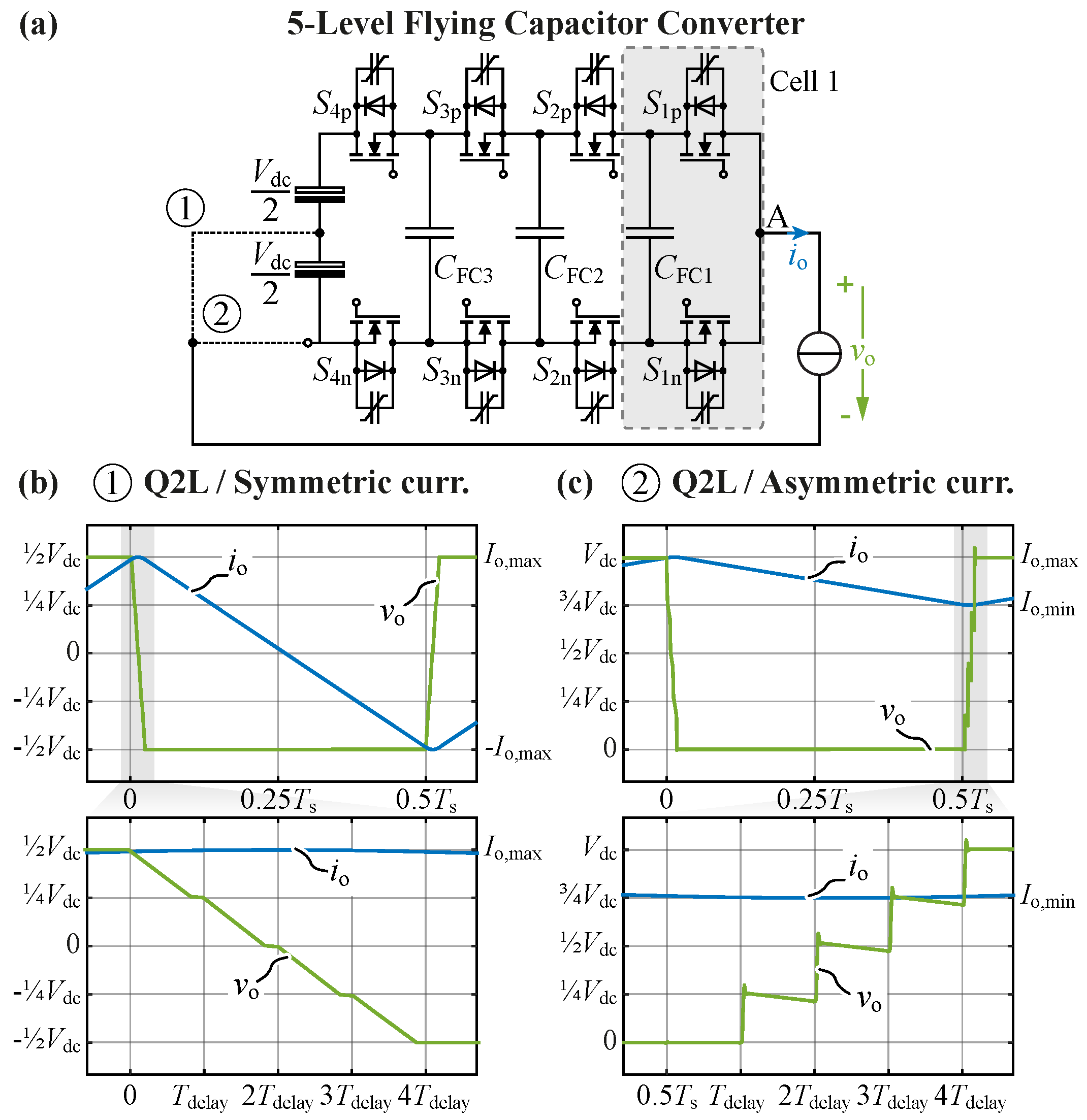
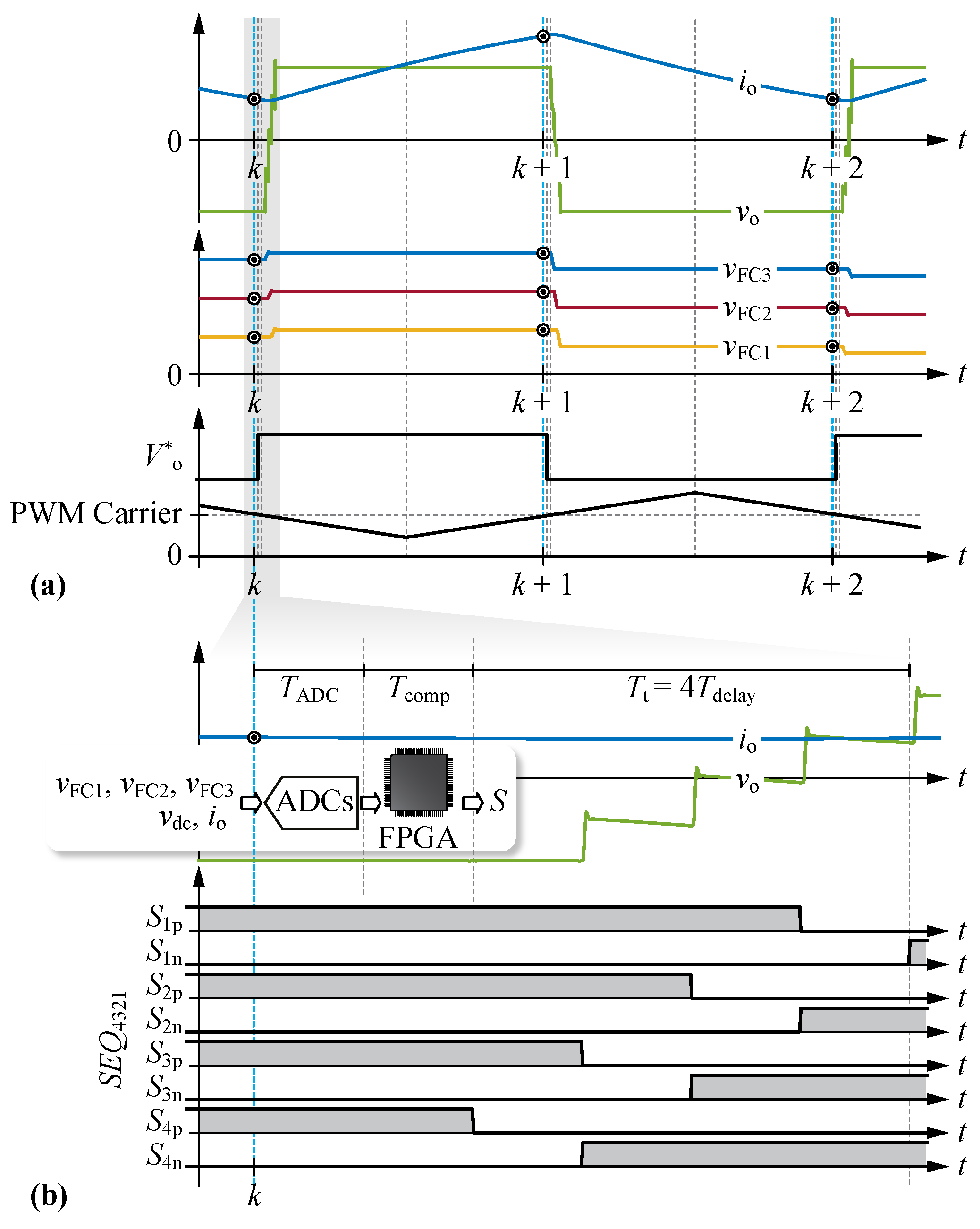
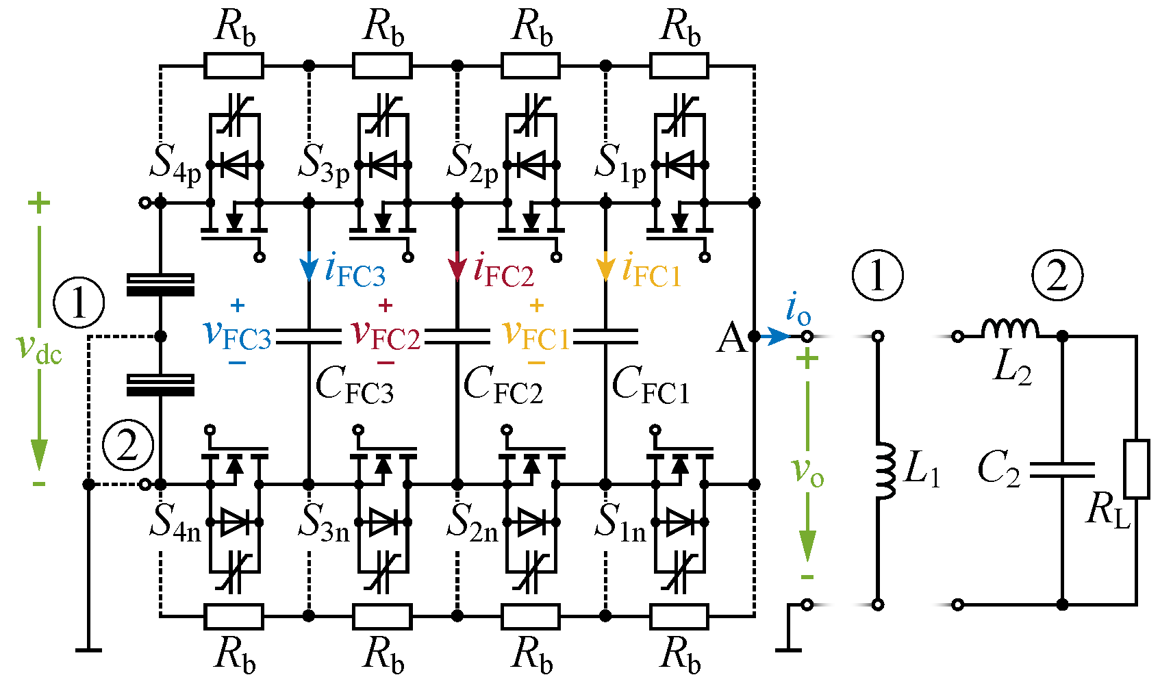
2. Q2L Operation of the 5L-FCC

This section recapitulates the processes in the Q2L-operated 5L-FCC for ZVS and HS transitions employing consecutive switching sequences described in [29]. Next, the analysis is extended by first considering also non-consecutive switching sequences and second including operation of the Q2L-FCC with zero output current. The in-depth analysis of the switching transitions given here is required to determine the total net charge exchange of the flying capacitors during Q2L transitions and ultimately to enable the development of a robust FC voltage balancing concept for Q2L-FCCs. Note that the obtained results are generic and apply to N-level Q2L-FCCs. However, we exemplify the considerations using a 5L-FCC (see Figure 1) for clarity. The corresponding circuit simulations employ an exemplary MOSFET equivalent circuit that consist of a voltage-controlled current source, the non-linear parasitic MOSFET capacitances, the antiparallel body diode, the diode reverse recovery, and the package inductances.

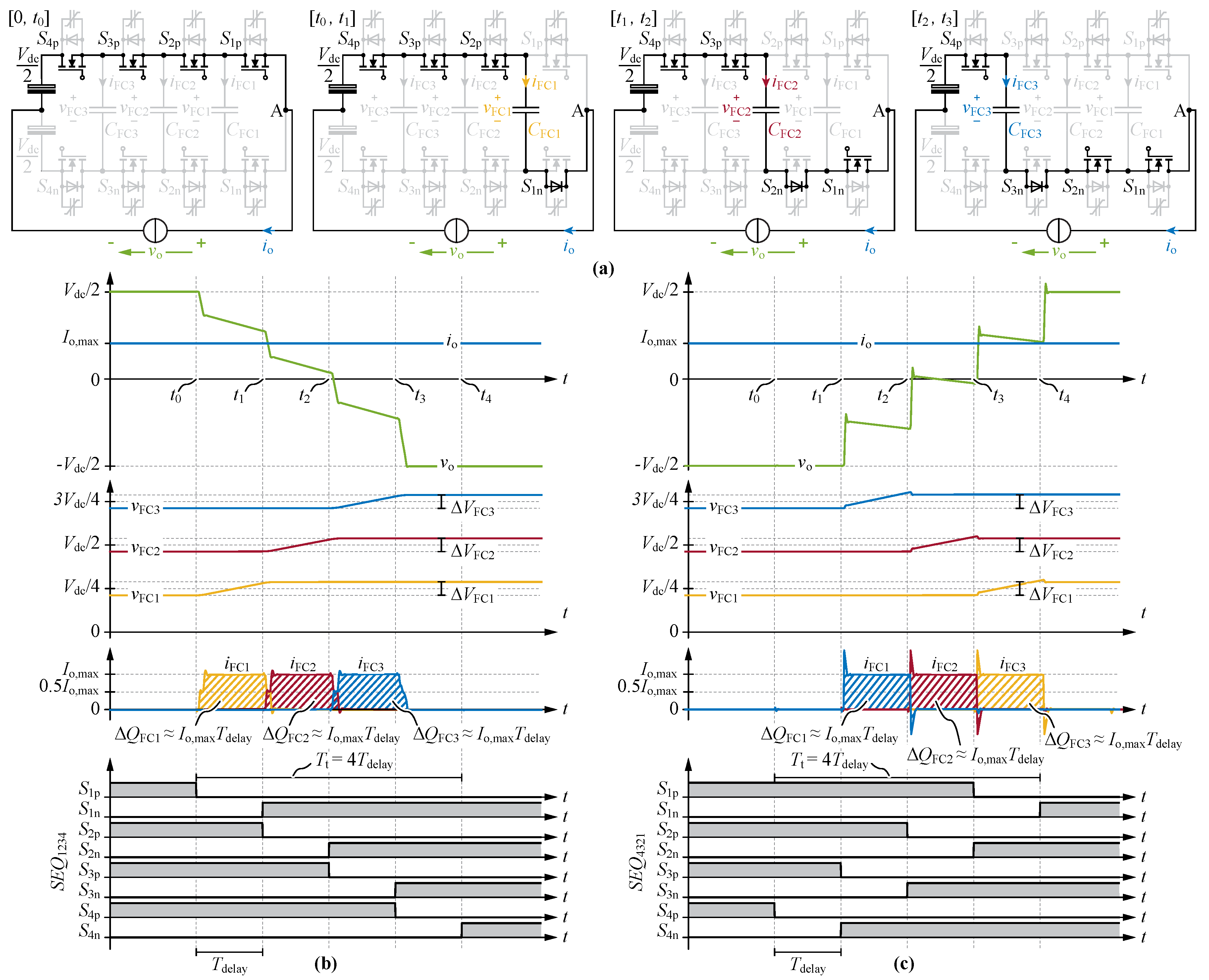
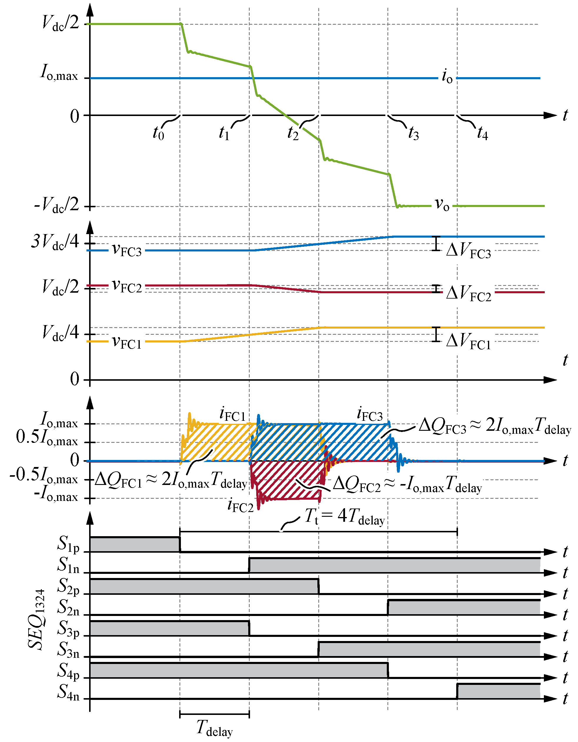
2.1. Operating Principle with Non-Zero Output Current

As it can be seen in Figure 1, a 5L-FCC consists of 4 cells (in general, an N-level FCC consists of n = N 1 cells), each comprising two complementary switches ( S x p and S x n ) and a flying capacitor ( C FCx ), whereas the cell which is the closest to the DC-link includes the DC-link capacitance. A Q2L (switching) transition is a commutation of the load current from all upper switches ( S 1 p - S 4 p ) in state on to all bottom switches ( S 1 n - S 4 n ) in state on, cf. Figure 1a, or vice versa. The bride-leg output voltage v o thus attains two distinct voltage levels ( V dc / 2 and V dc / 2 ) for most of the time and the several intermediate voltage levels appear only shortly during the Q2L transitions. A Q2L transition is characterized by a switching sequence ( S E Q ) that defines the order in which the individual cells are commutated. For example, in a 5L-FCC S E Q 1234 means that the cells are commutated consecutively starting from cell 1 and ending with cell 4, see Figure 2a.
Figure 2a illustrates such a Q2L transition and defines selected time intervals for the example of a falling slope of v o , positive output current i o and S E Q 1234 which results in ZVS transitions for all switches. Figure 2b shows the simulated key waveforms of this transition. Similarly, Figure 2c shows key waveforms for a HS transition, i.e., constant positive output current ( I o , max ) during the switching transition with positive slope of v o and S E Q 4321 . For a more in-depth description of processes in the sub-intervals of ZVS and HS commutations we refer to [29].
Note that consecutive sequences, i.e., S E Q 1234 or S E Q 4321 , lead to FC charge increments given by
| Δ Q FC { j } | T delay { j } | I o , max | ,
where j is the number of the FC and T delay is the time allocated for the transition of an individual cell. Note that the selection of T delay is discussed in detail in Section 2.3. To facilitate the modeling and balancing of FC voltages, we assume equal delay times T delay for all cells and thus identical base charge increments result:
Δ Q FC 0 = Δ Q FC 1 = Δ Q FC 2 = Δ Q FC 3 T delay I o , max .
It is worth noting that the transferred charges are independent of the switching frequency and the number of levels. However, the sign of the net charge exchange of an FC during a Q2L transition for a given sequence depends on the sign of the load current and the direction of the voltage slope.
For FCC realizations with more than two cells, i.e., n > 2 ( N > 3 ), the cells can also be switched in a non-consecutive manner and thus a total of ( n ! ) different consecutive and non-consecutive sequences exists. The subset of non-consecutive sequences contains ( n ! 2 ) sequences. Figure 3 presents an example of a Q2L transition with the non-consecutive sequence S E Q 1324 : FC1 and FC3 are charged with 2 Δ Q FC 0 , whereas the FC2 is discharged with Δ Q FC 0 . Therefore, in contrast to consecutive sequences, non-consecutive sequences lead to non-equal charge exchanges of the individual FCs (for the same T delay and I o , max ). Therefore, even charging of some FCs and discharging of others during the same Q2L transition can be achieved. Note, however, that all FCs experience a charge exchange, and hence are coupled through a sequence in the sense that it is not possible to influence only a selected subset of the FCs.
Considering the exemplary 5L-FCC, Table 1 summarizes all sequences, denoted henceforth as set S CL , and their effects on the FCs’ charge for the case of ZVS transitions. It is found that for the HS transition, the sequences have opposite effect. Therefore, the values from Table 1 need to be multiplied by (−1) to obtain the charge increments for HS transitions. Furthermore, Table 1 is simplified by utilizing symmetry, i.e., the fact that sequences S E Q 3 xxx and S E Q 4 xxx result in the same absolute values of total charge exchanges as S E Q 2 xxx and S E Q 1 xxx , respectively. However the order of FCs and delay times is reversed, and the values from the table must be multiplied with ( 1 ) to obtain the actual FC charge exchanges, which is denoted by the − sign preceding the sequence’s name (see right & bottom labels in Table 1).
Based on this analysis, we formulate the total change of charge provided to the FCs as
Δ Q FC = Δ Q FC 1 Δ Q FC { j } = I o , max ( S × T delay ) ,
where
T delay = T delay 1 T delay { n } T
is a delay time vector and S is a matrix which specifies how the particular delay times influence the charge change of the FCs and is equivalent to the rows in Table 1. The matrix S is constructed by stacking the effects that the sequence has on each FC, hence it has dimensions of j × n . From Table 1 it is apparent that the charge increments can be equal to values from the following set: ± Δ Q FC 0 · { 1 , 2 , , j } . In order to ensure well defined voltage levels across the switches and ease of balancing, equal values C FC of all FCs are selected, which consequently leads to the voltage increments
Δ V FC = Δ V FC 1 Δ V FC { j } = Δ Q FC C FC .
Henceforth, for the sake of simplicity, we will consider equal delay times T delay for all cells, and the implications of that assumption are discussed further in Section 4. Taking as an example the sequence S E Q 1324 (cf. Figure 3) and equal delay times T delay we obtain:
Δ V 1324 = I o , max C FC 1 0 1 0 0 0 1 0 0 1 1 0 × T delay T delay T delay T delay ,
Δ V 1324 = Δ Q FC 0 C FC 2 1 2 .
which corresponds to the FC voltage waveforms in Figure 3.

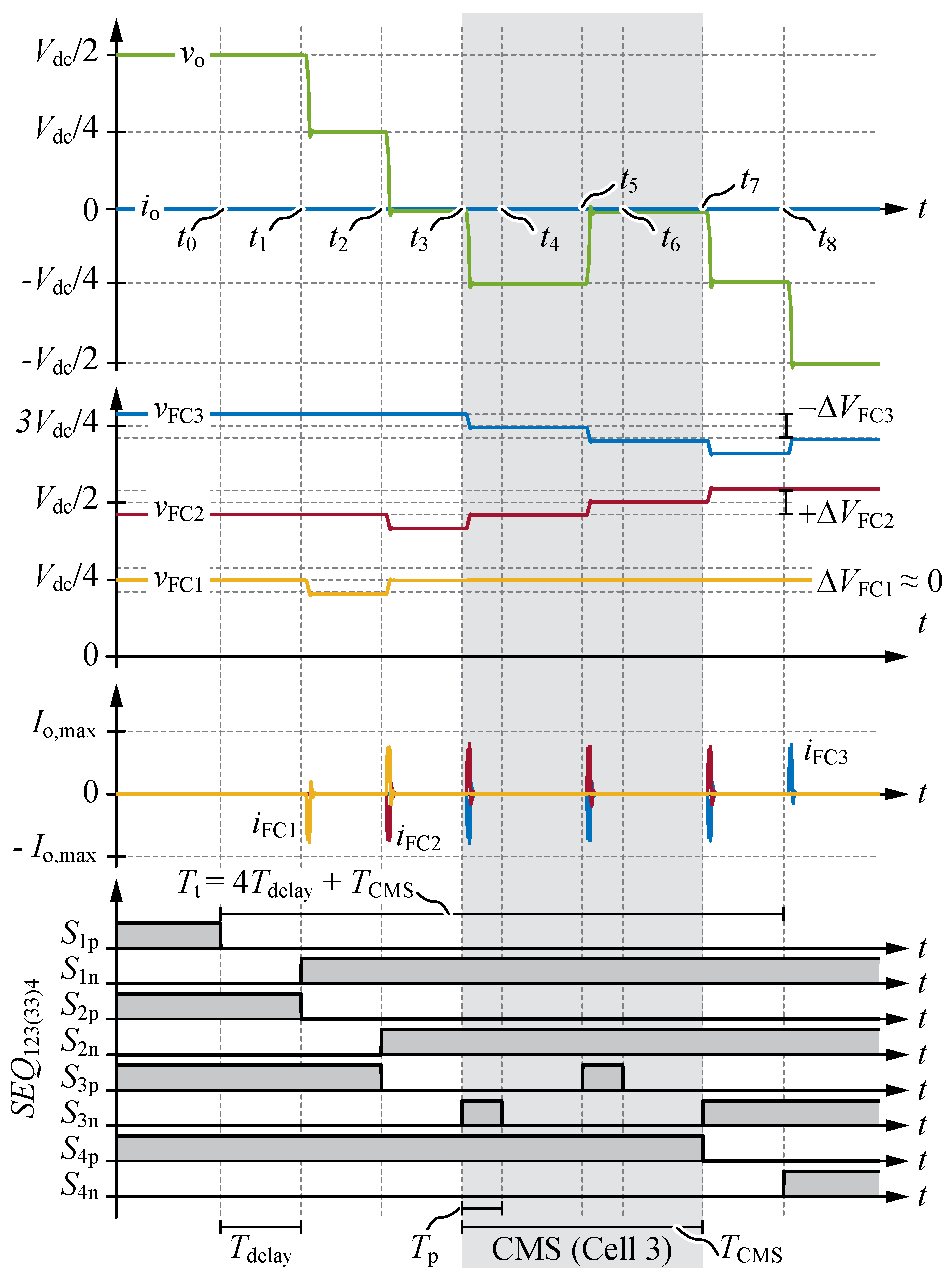
2.2. Operating Principle with Zero Output Current: Cell Multiple Switching

From (3) it is obvious that in case of zero output current, the charge increments of the FCs are expected to be zero. Figure 4 presents the simulation results for Q2L operation with i o = 0 during the switching transition with negative slope of v o . It can be seen that during each commutation, due to the hard-switching and charging of the switches’ output capacitances, the commutation loop current leads to an exchange of charges, i.e., subtraction of charge from a cell’s input-side capacitor and addition of charge to the output-side capacitor of the respective converter cell. This can be seen, e.g., in Figure 4 between t 2 < t < t 3 where the exchange of charges between FC1 and FC2 occurs. Note that in case of zero-current switching of cell 1, the charge is delivered to the load, whereas in case of cell 3, the charge delivered to FC3 is subtracted from the DC-link. For an in-depth analysis we refer to [40]. However, the net charge exchange of each FC over the entire transition is approximately zero. Nevertheless, the exchange of charge between the FCs during no-current Q2L transitions can be utilized in a novel method for balancing the FC voltages in case of zero output current.
To do so, we insert additional commutations in one or more cells during a Q2L transition. This leads to additional hard-switching events of one or several of the MOSFETs. This concept that we refer to as cell multiple switching (CMS) thus allows to obtain non-zero net charge exchange of certain FCs over a Q2L transition, therefore offering a means of balancing the FC voltages even in case of zero output current.
Figure 5 shows the exemplary simulation results for a 5L-FCC in split DC-link configuration with zero output current during the Q2L transition with negative slope of v o and a CMS event inserted in cell 3. It can be noticed that until t < t 3 the processes in the transition occur as for a sequence S E Q 1234 (see Figure 4). However, at t = t 4 , S 3 n turns off and the circuit remains in steady-state during [ t 4 , t 5 ] and v o = V dc / 4 applies. The time interval between t 3 and t 4 , in which S 3 n is on, has a duration of one pulse time T p . Two additional switching operations are inserted between t 5 < t < t 8 : First, v o is switched back to 0 during t 5 < t < t 7 , and, subsequently, v o is switched to V dc / 4 during t 7 < t < t 8 . During t 3 < t < t 4 , the charge of FC2 is increased by Δ Q S 3 p and FC3 is discharged by the same value, where
Δ Q S 3 p = Q oss , 3 p + Q rr , 3 p ,
with Q oss , 3 p and Q rr , 3 p being the charges stored in the output capacitance C oss of the MOSFET and the reverse-recovery charge of the anti-parallel diode, respectively. During t 5 < t < t 6 , FC2 is again charged, whereas FC3 is discharged by Δ Q S 3 n . Finally, at t = t 8 , S 4 n turns on and the last commutation is completed. It can be seen that the presented sequence introduces two additional switching pulses in cell 3, therefore it is denoted as S E Q 123 ( 33 ) 4 , where subscript (33) denotes the CMS event in cell 3.
Assuming that the charge increment from each switch is approximately the same and equal to Δ Q S , a CMS event results in total net charge increment of the affected FCs equal to:
Δ Q FC 2 Δ Q S .
The corresponding voltage increment per CMS event is thus:
Δ V CMS Δ Q FC C FC 2 Δ Q S C FC .
Using the linear charge-equivalent output capacitance C Q , eq and assuming that Q rr 0 , (10) can be further simplified to:
Δ Q S = 0 V ds C oss ( v ) · d v = C Q , eq · V ds ,
Δ V CMS 2 C Q , eq · V ds C FC .
Therefore, the CMS balancing controllability depends on the capacitance ratio k c = 2 C Q , eq / C FC and is discussed in detail for semiconductors of different voltage classes in Appendix A.

2.3. Duty Cycle Limitation/Selection of T delay

For a certain output current I o , max the charge increments of the FCs during a Q2L transition are proportional to the delay times, see (3). Hence this parameter is a degree of freedom in the design of Q2L-FCCs and its constraints are discussed in the following. The duration T t of a complete Q2L transition, cf. Figure 2b,c, in the NL-FCC is given by
T t ( N 1 ) T delay ,
4 T delay , for N = 5 .
Thus, the Q2L transitions limit the maximum duty cycle to
d max = 1 2 T t T s ,
= 1 8 T delay T s , for N = 5 .
Therefore, the delay time can be selected only within certain boundaries
T delay [ T min , T max ] .
The maximum boundary T max follows from the allowable duration of the switching transition, i.e., from the application-specific d max , given that increased commutation times decrease the available output voltage-time product. The minimum boundary T min follows from the system’s physical limitations, i.e., the required interlock delay time to prevent shoot-through events. In practical applications additional constraints can be considered, e.g., in soft-switching Q2L-FCCs the time required to achieve ZVS in partial-load operation increases T min above the minimum required to prevent shoot-through.
Note that if CMS is activated in the Q2L-FCC, the duration of the transition increases due to the inserted additional pulses. In case of inserting n CMS events of duration T CMS (cf. Figure 5), the transition time is:
T CMS 2 n CMS ( T p + T delay ) ,
T t ( N 1 ) T delay + T CMS ,
6 T delay + 2 T p , for N = 5 , n CMS = 1 .
Therefore, based on the application specific d max , the allowable number of CMS events, the number of involved cells, and T p must be defined together with T delay .

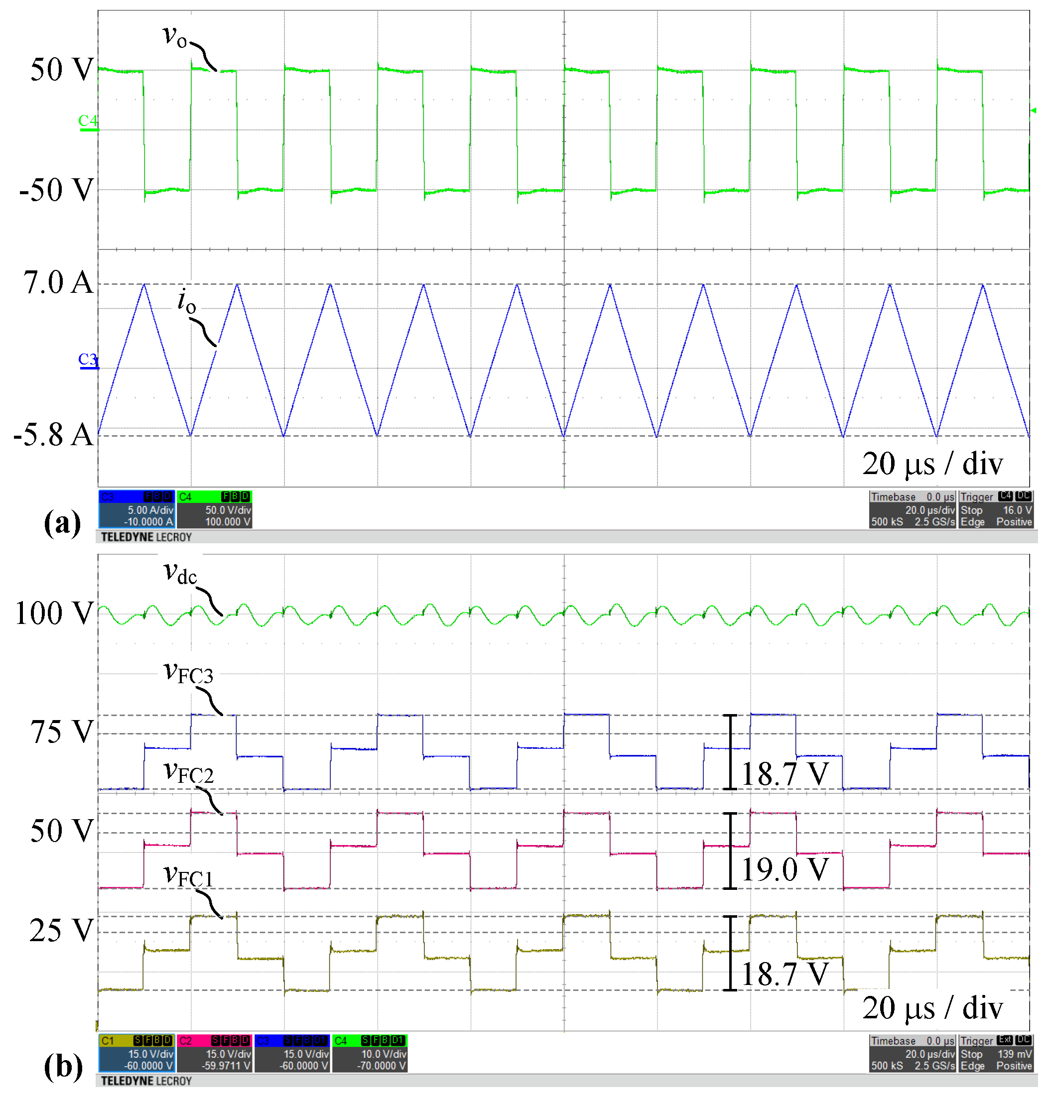
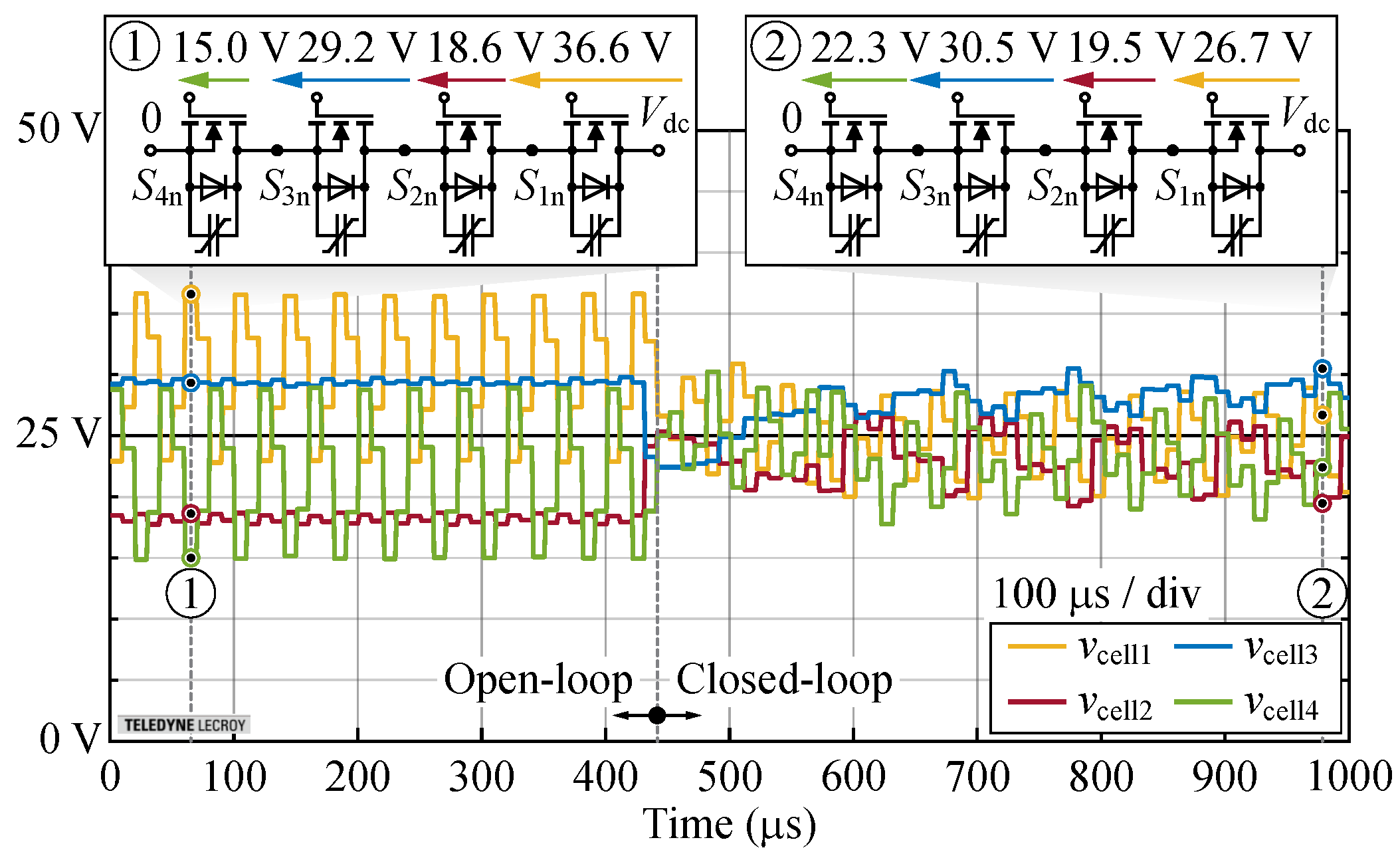
3. Open-Loop FC Balancing

As described earlier in [29], the balancing of the FC voltages can be achieved with a passive modulation that employs consecutive sequences, hence either by charging or discharging all FCs with the same charge increment during a Q2L transition, see Table 1. For a versatile HB realization, i.e., designed for operation with asymmetrical or symmetrical output currents, the following modulation scheme has been proposed:
S OL = { S E Q 1234 , S E Q 1234 , S E Q 4321 , S E Q 4321 , } .
The scheme results in open-loop balancing over two switching periods (4 Q2L transitions). However, the maximum peak-to-peak voltage ripple is
Δ V pp 2 T delay · I o , max C FC ,
due to the charging characteristic with asymmetric currents. Please refer to [29] for an in-depth discussion.
While in principle this modulation scheme is sufficient to achieve balanced FC voltages, the controllability is limited and results in a non-optimal FC voltage ripple. Advantageously, this approach does not require FC voltage measurements. On the other hand, balancing resistors connected in parallel to the switches are necessary to ensure balanced FC voltages in case of zero output current. We refer to this approach as open-loop (OL) balancing and provide experimental evaluation in Section 6.2.

4. Load-Independent Closed-Loop Balancing

In this section we propose a concept for load-independent closed-loop (CL) balancing. The most straightforward approach is to implement a controller which uses measurements of the FC voltages and of the output current to achieve close tracking of the FC voltage references. However, as indicated in [32] due to the opposite voltage ripple on FCs, the switches can be operated with a strong asymmetry of the blocking voltages. To address this issue, alternatively the controller can be built to equalize the cell voltages, derived as differences between the voltages of capacitors adjacent to the switches, and hence ensuring equal voltage sharing among the series-connected switches. We present the two aforementioned approaches in detail in Section 4.1. Furthermore, the proposed balancing concept is eventually implemented and tested (see Section 6) up to the nominal output current of the FCC; for the discussion of extreme load cases, i.e., an overload and short-circuit currents we refer to Appendix B.
Figure 6a shows the block diagram of an FCC HB with Q2L voltage balancing controller. The measured HB output current i o is fed to the output quantity controller which specifies the reference output voltage V o for the modulator and the Q2L voltage balancing controller. The design and realization of the output quantity controller is decoupled from Q2L operation and not within the scope of this paper. For that reason, the considered Q2L-FCC is operated with a fixed duty cycle of d = 50 % in the following.
As mentioned before, a given switching sequence affects several FC voltages, i.e., they are coupled through the selection of the sequences. Therefore, controlling all FC voltages is a multiple-input multiple-output (MIMO) control problem. MIMO systems can be easily addressed by model predictive control (MPC) which is formulated in the time domain [41,42]. Therefore, we use MPC with reference tracking to realize a Q2L voltage balancing controller.
Essentially, based on the slope of the reference output voltage V o , the measured FC voltages v FC 1 , …, v FC j , the measured output current i o , and the DC-link voltage v dc , the Q2L voltage balancing controller selects a switching sequence S E Q and respective times T delay , T p , which are the input to the actual Q2L modulator. Figure 6b presents the detailed block diagram of the controller which contains two distinct parallel paths (sub-controllers), i.e., one for control without load current using CMS ( i o = 0 , based on FC voltage tracking, see Section 4.1.1) and one for operation with non-zero load current ( | i o | > 0 , based on cell voltage tracking, see Section 4.1.2). The implementation of these sub-controllers is explained in the following subsections. In the last part of the Q2L controller, based on the value of i o , the multiplexer decides which of the two sub-controllers is activated.
Ultimately, both controllers define a certain commutation sequence ( S E Q ) for a given Q2L transition (e.g., S E Q = 123 ( 33 ) 4 for the example shown in Figure 4) and also the values for T delay and T p to be used. During the Q2L transition, the modulator translates this information into gate signals for the individual switches according to the state machine shown in Figure 7.

4.1. Closed-Loop Control with Non-Zero Output Current

In [29] we have proposed an active method for FC voltage balancing in a Q2L-3L-FCC. This method relies on the determination of an optimal ripple of v FC and then the computation of individual delay times that eliminate any voltage ripple error in the next transition, similarly to a deadbeat controller. This method is however complex and computationally expensive for FCC realizations with N > 3 : For each of the ( N 1 ) ! available sequences, ( N 1 ) different delay times for ( N 2 ) FCs need to be considered. For that reason, in this work we propose a different approach that still utilizes all available sequences. However, to limit the degrees of freedom, we make the following simplifications:
  • All delay times in a given switching transition are equal, i.e., T delay 1 = T delay 2 = T delay 3 = T delay 4 = T delay .
  • Two discrete delay time values are used: T delay { T min , T max } , where T min is intended to be selected by the controller in the steady-state in order to keep the voltage ripple small. On the other hand, T max is selected in cases of significant unbalance to reduce the error more aggressively.
For the exemplary 5L-FCC, there are thus only 48 different possible actions that the controller needs to consider (24 unique sequences × 2 unique delay times). Note that with a higher number of levels, the number of possible actions increases substantially, as does the computation effort. However, to reduce the computation effort, the solution to the optimization problem can be solved offline and stored in a look-up table (LUT), see more details of implementation presented in Section 4.2.
As presented in Section 2.1 the charge increments in the FCs occur during the switching transition only, whose duration is relatively short compared to the switching period. Therefore, a discrete time domain with constant sampling interval k ( 0.5 T s ) is defined, where k N denotes the time steps, cf. Figure 8a. Note that this simplified expression is valid for a fixed duty cycle of 50% only. For realizations with variable duty cycle, the sampling intervals would need to be changed such that the sampling instants coincide with the Q2L transitions. Figure 8b shows the timing of the measurement data acquisition and the control routine execution in the FPGA within the highlighted Q2L transition. It can be noticed that the measured value of the output current is delayed by a measurement delay T ADC due to analog-to-digital conversion (ADC). Furthermore, T comp denotes the delay resulting from performing the required computations in the FPGA. For the experimental system considered in this paper (cf. Section 5 for details) the total delay amounts to approx. 600 ns and the deviation between the measured current used for the controller execution and the current value present during the actual switching transition is found to be less than 2.6%; therefore we do not employ delay compensation.

4.1.1. FC Voltage Tracking

In this approach the proposed MPC relies on the model of the voltage increment (cf. (5)) to predict the future FC voltages,
V FC ( k + 1 ) = V FC ( k ) + Δ V FC ( k ) ,
where
V FC = v FC 1 v FC { j } T
and it depends on the available control actions and input variables:
Δ V FC ( k ) = f 1 ( V o , S CL , T delay , i o ) ( k ) .
In order to keep the computation effort low and eliminate the need to predict the future output current, a one-step prediction horizon is used, i.e., N p = 1 , which is found to provide sufficient performance. The control problem at time step k of tracking the FC voltage reference can be mapped into the cost function:
J 1 = [ ( V FC V FC ( k + 1 ) ) 2 ] ,
using the squared 2-norm, where
V FC = V dc N 1 1 2 j T
= V dc 1 / 4 1 / 2 3 / 4 T , for N = 5 .
Using the squared 2-norm, possible control actions that would lead to large voltage deviations and hence poor reference tracking are heavily penalized, which ultimately ensures good tracking performance. The optimization problem can be stated as
[ S E Q opt ( k ) , T opt ( k ) ] = arg minimize J 1
subject to T delay 1 1 , n × { T min , T max }
S E Q ( k ) S CL

4.1.2. Cell Voltage Tracking

In the second approach, to ensure well defined voltage levels across the switches, the controller is built to equalize the cell voltages,
V cell = v FC 1 v FC 2 v FC 1 v dc v FC { j } ,
instead of the FC voltages. Note that unlike the FC voltages, all cell voltages are ideally equal. Using the cell voltage increments defined as
Δ V cell = Δ V cell 1 Δ V cell 2 Δ V cell { n } = Δ V FC 1 Δ V FC 2 Δ V FC 1 Δ V FC { j } ,
the MPC can predict the cell voltages at the next time step as
V cell ( k + 1 ) = V cell ( k ) + Δ V cell ( k ) ,
which, similar to (25), depends on the available control actions and input variables
Δ V cell ( k ) = f 2 ( V o , S CL , T delay , i o ) ( k ) .
The function f 2 maps the sequences to effects on the cell voltage increments in dependence of the delay times based on Table 1. Consequently, the following cost function describes the control problem of tracking the cell voltage references at time step k:
J 2 = [ ( V cell V cell ( k + 1 ) ) 2 ] ,
where
V cell = V dc n × 1 1 , n .
Finally, the optimization problem is stated as (29), however in this case minimizes the cost function J 2 . Both proposed control targets, i.e., tracking of FC voltages or cell voltages, result in good FC voltage balancing performance. However, the cell voltages controller ensures more balanced and symmetrized switch voltages and is used in experiments presented in Section 6.
Regarding implementation (cf. Figure 6b), first a pre-processor computes (32)–(33), i.e., based on the required V o slope, the sign of i o , the expected cell voltage increments Δ V cell for all combinations of sequences (cf. Table 1) and { T min , T max } are computed and the cell voltages at time step k + 1 are predicted. Next, the cost function (34) is evaluated and the optimization problem (29) for J 2 solved, resulting in the selection of the control action (i.e., one sequence and either T min or T max ) with the minimum cost, i.e., leading to cell voltages at time step k + 1 that are as close as possible to the reference values. Note that Table 1 shows the effect on charge increments for the ZVS-type of transitions, therefore, in the last step, the post-processor by using the symmetry, adapts the signs if the next transition is of HS-type instead (note that the transition type follows from the desired output voltage change and the output current direction). In the prototype system described below in Section 5, this control algorithm has been implemented in a high-performance Xilinx Zynq Z-7020 SoC.

4.2. Closed-Loop Control with Zero Output Current

As discussed above in Section 2.2, CMS can be utilized to charge/discharge FCs even in case of zero output current. The following assumptions are considered for the realization of the corresponding CMS-based controller, i.e., the second path shown in Figure 6b:
  • The delay times T delay are set to the minimum value T min as their duration does not impact the balancing when i o = 0 .
  • Similarly, the sequence of the switching actions within a Q2L transition does not influence the total voltage increments when i o = 0 . Therefore only the sequence S E Q 1234 is used for simplicity when CMS is active.
  • The pulse time T p of a CMS event must be sufficiently long for a zero-current HS transition to complete. Therefore, we set T p = T min .
Note that using short delay and pulse times is preferable to minimize the overall transition times T t .
The analysis presented above in Section 2.2 indicates that theoretically there is an infinite number of ways to insert CMS events if the number of events inserted per Q2L transition is not limited. However, practically, it is desirable to keep the number of CMS events per transition low (duty cycle limitation) and it is found that for the considered exemplary 5L-FCC a selection of only 6 CMS sequences (given in Table 2) is sufficient to achieve robust controllability. The reasoning behind the selection of these CMS sequences is explained in the following.
Interestingly, it can be seen from Table 2 that inserting a CMS event in the m th cell leads to a discharge of FCm (in case of m = n , the energy is exchanged with the DC-link capacitor), and charges FCm−1 (for m = 1 there is no FC to charge). Furthermore, the CMS events can be superimposed to achieve desired charge increments, e.g., events ‘0001’ and ‘0010’ inserted over two subsequent Q2L switching transitions yield the same effect as the same two events ‘0011’ within one Q2L transition. However, the latter results in a longer Q2L transition time and hence a reduction of the available duty cycle. This characteristic can be used to obtain individual balancing of FCs (charge/discharge) over two Q2L transitions. Note that in the following design of the controller, for flexibility reasons, we use all CMS events shown in Table 2.
Similar to the approach used in case of non-zero output current, again we employ an MPC with reference tracking over a finite prediction horizon, but in this case of length N p = 6 , to accommodate the aforementioned superposition of CMS events in the controller. Moreover, we use FC voltage tracking (not cell votlage tracking), because for zero output current operation, no large voltage ripples occur. Based on Table 2 the set of available CMS sequences is defined as
U = { 0001 , 0010 , 0100 , 1000 , 0011 , 1100 } .
We introduce a vector of CMS sequences for the considered prediction horizon:
U ( k ) = u ( k ) u ( k + 1 ) u ( k + N p 1 ) .
The prediction model of FC voltages is
V FC , CMS ( k + 1 ) = V FC ( k ) + Δ V CMS ( k ) ,
Δ V CMS ( k ) = f 3 ( U ) ( k ) .
The control problem can be described by the cost function
J 3 = l = k k + N p 1 [ [ ( V FC V FC , CMS ( l + 1 ) ) 2 ] ] ,
and the solution to the optimization problem is the choice of U ( k ) that minimizes this cost function J 3 :
U opt ( k ) = arg minimize J 3
subject to l = k , , k + N p 1
U ( k ) U
where U is the N p times Cartesian product of the set of CMS sequences U , cf. (36). Following the principle of receding horizon policy, only the first element of the optimal CMS sequence U opt ( k ) is applied at time step k, and another optimization is performed at the next time step.
The CMS controller (cf. Figure 6b) relies on the solution to the optimization problem (41) which is solved offline: The FC voltage errors ( V FC V FC ) as well as the expected voltage increments Δ V CMS are normalized by the capacitance ratio k c (cf. Section 2.2) and then stored in a look-up table (LUT) for the considered voltage error range. In the online implementation, the CMS pre-processor computes the voltage errors ( V FC V FC ( k ) ) and normalizes them. This information is fed to the MPC block which retrieves the optimum solution from the precomputed LUT in the FPGA’s memory. To avoid unnecessary CMS activation, especially when the FC voltages are close to the references (small errors), a voltage hysteresis is considered. Again, the online part of the algorithm has been implemented in a high-performance Xilinx Zynq Z-7020 SoC.

5. Hardware Implementation

In order to validate the proposed concepts, a LV proof-of-concept hardware demonstrator of a 5L-FCC HB has been designed according to the schematic presented in Figure 9. Depending on the connection of the load, two types of operation can be achieved (see also Figure 1): ➀ Symmetrical output current with ZVS transitions, and ➁ asymmetrical output current ZVS and HS transitions. In order to test OL balancing, resistors R b can be placed in parallel to the switches.
Figure 10 shows the photos of the realized 5L-FCC bridge-leg demonstrator and Table 3 summarizes the main specifications and the selected control parameters. Even though 150 V GaN e-FETs are used (EPC2033) and hence a DC link voltage of up to 400 V would be possible, all experiments have been carried out with a reduced DC-link voltage of 100 V for safety reasons. Note that the DC voltage level does not impact the validity of the experimental verification (see also Appendix A). The converter is operated with 50 kHz switching frequency and a fixed 50% duty cycle. For demonstration purposes, a relatively large maximum peak-to-peak FC voltage ripple of 20 V is selected. With a maximum output current of 6.6 A and a maximum delay time of 100 ns, the required capacitance value of the FCs is 66 nF, see (22). The FCs are realized with C0G ceramic capacitors due to their linearity (1 kV CAA572C0G3A663J640LH).
The FC voltage measurement circuitry is placed on a separate PCB that is mounted on top of the main power board (cf. Figure 10a) and it can be disconnected for the tests with OL balancing. The power board, cf. Figure 10b contains the switching-cell daughter boards (carrying the GaN eFETs) on top and the FCs on the bottom. Furthermore, it contains the DC-link voltage and output current measurements circuitry. The Q2L controller and modulator are implemented in a high-performance Xilinx Zynq Z-7020 SoC.

6. Measurement Results

This section presents experimental results obtained with the 5L-FCC hardware demonstrator introduced in Section 5. In order to demonstrate the Q2L operation and the proposed concepts for FC voltage balancing, two synchronized LeCroy HDO4054A 12-bit oscilloscopes are used to measure waveforms of the DC-link voltage ( v dc ), all FC voltages ( v FC { 1 , 2 , 3 } ), and the half-bridge output voltage ( v o ) as well as the output current ( i o ), see Figure 9. Consequently, for each experiment two (temporally aligned) oscillograms are presented. Unless stated otherwise, resistive balancers R b = 30 k Ω are connected in parallel to the switches.

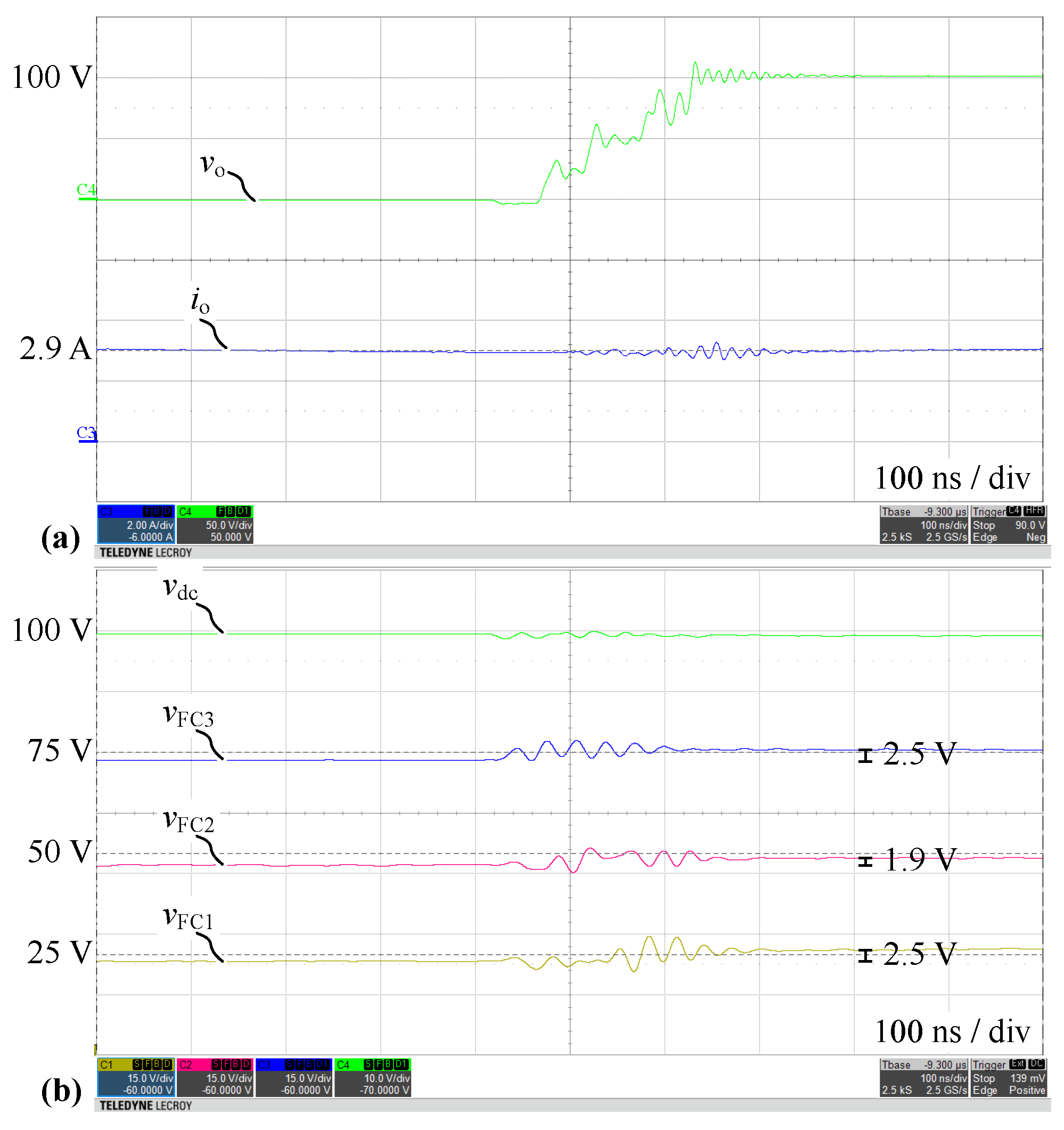
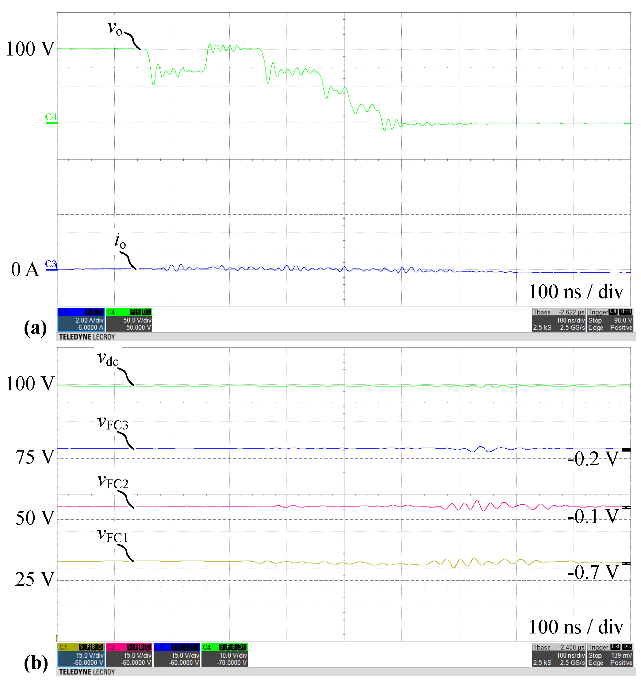
6.1. Q2L Transitions

First, Q2L output voltage transitions are analyzed to confirm the Q2L operation and the description of charge and voltage increments presented in Section 2. Figure 11 shows measured waveforms during the switching transition with a positive slope of v o and negative output current ( i o I o = 5.9 A ), which results in a ZVS transition. Figure 12 shows waveforms of the switching transition with a positive slope of v o and positive output current ( i o I o = 2.9 A ), which results in a HS transition. Based on the employed delay times and FC capacitance values, the voltage increments are calculated according to (5) and compared with the measured voltage changes (see oscillograms). The average absolute relative deviation of the estimated from the measured voltage changes is 3.7% for ZVS (cf. Figure 11) and 13.3% for HS (cf. Figure 12), thus confirming good accuracy of the estimation.
Figure 13 shows an exemplary CMS sequence S E Q 1 ( 11 ) 234 (events in cells ‘1000’) during a switching transition with negative slope of v o and zero output current. It can be seen that the voltage change of FC1 is about −0.7 V, whereas the expected voltage change calculated with (12) is −0.8 V, again showing good agreement with a deviation of 13% between calculation and measurement. Moreover, it can be noticed that also the voltages of FC2 and FC3 change slightly, i.e., by −0.11 V and −0.19 V, respectively, which is due to the non-idealities of the circuit.

6.2. Open-Loop Balancing

Next, we present measurement results confirming the OL balancing concept proposed in [29] and briefly described in Section 3. The modulation scheme from (21) is implemented with T delay = 100 ns for all cells. Consequently, all of the capacitors are charged/discharged with the same charge value in each transition, and open-loop balancing over two fundamental switching periods is achieved.
Figure 14 shows measured waveforms for split DC-link configuration with OL balancing and triangular current ( I o , max = 7.0 A , I o , min = 5.8 A ). The average absolute relative deviation of the estimated peak-to-peak voltage ripple (19.4 V, cf. (22)) from the measured value is 3%, which corroborates the proposed model. However, note that in steady-state the mean values of the FC voltages deviate from the reference values (cf. (27)), on average by 4.9 V (15%). This is a consequence of the circuit’s equivalent impedances formed by the switches and the resistive balancers.
Figure 15 presents measured waveforms for full DC-link configuration with OL balancing during a negative load step from 100% to 67% of the nominal load ( I o = 4.6 A 3.0 A , Δ I pp = 4 A ). Note that balancing is maintained despite the transient at the FCC bridge-leg’s output. It can be concluded that even without closed-loop voltage balancing, load steps within the nominal load range are not critical regarding FC voltage balancing thanks to correctly dimensioned FCs.

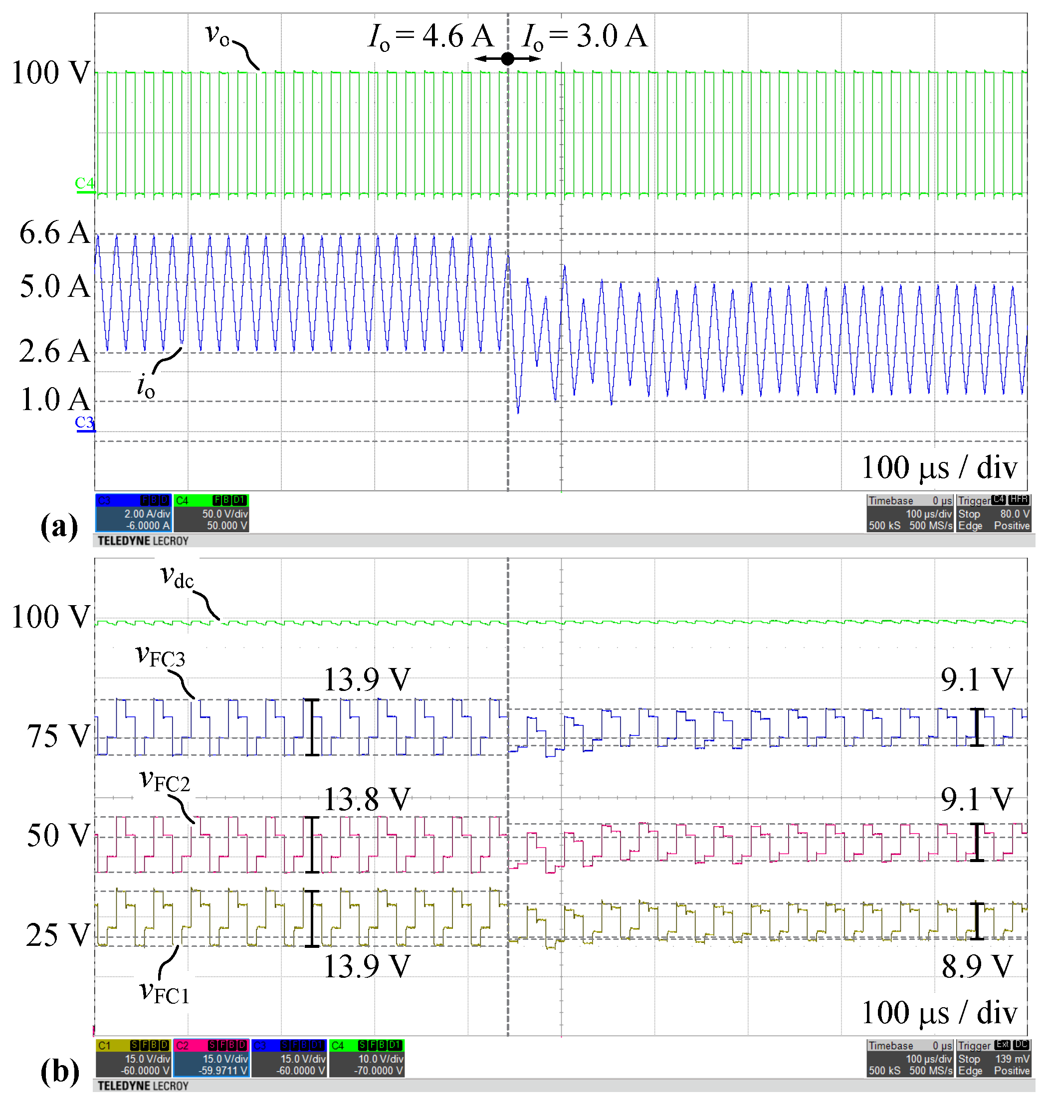
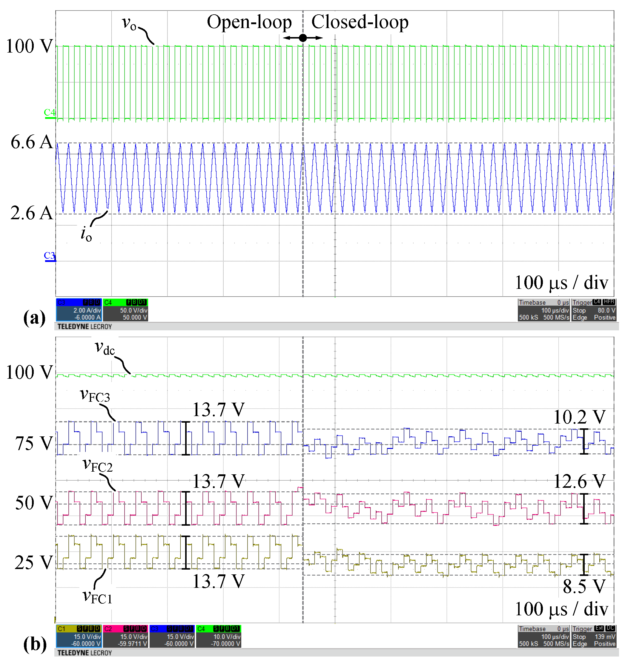
6.3. Closed-Loop Balancing

This section presents experimental verification of the CL balancing concept proposed in Section 4. First, operation with non-zero load currents is demonstrated, cf. Section 4.1, where the cell voltage tracking MPC with horizon one, see (31)–(35), is employed and T delay = { 50 , 100 } ns for all cells is used. Next, for the operation with zero load current, the FC voltage tracking MPC with a horizon of six steps ( N p = 6 ) is employed, see (36)–(41), and T delay = T p = 50 ns are used, cf. Section 4.2.

6.3.1. Balancing with Non-Zero Output Current

Figure 16 shows measured waveforms for split DC-link configuration with CL balancing and triangular current ( I o , max = 5.9 A , I o , min = 5.8 A ). The average absolute relative deviation of the estimated peak-to-peak voltage ripple (4.5 V) from the measured value is 11%, which again corroborates the proposed model. Note that compared to OL balancing, an approx. 4 × smaller peak-to-peak voltage ripple is achieved for the following two reasons. First, with CL balancing in steady-state a minimum delay time ( T delay = 50 ns ) is selected by the optimization, whereas with OL balancing the FCs operate with voltage ripples that are characteristic for the maximum delay time ( T delay = 100 ns ), which is a consequence of the need to account for the the worst-case output current type (cf. Section 3). Second, in OL operation balancing occurs over 4 output voltage transitions, cf. (21), whereas in CL balancing, the optimization is carried out in every transition, ensuring minimum FC voltage ripple. Furthermore, under CL voltage balancing, the mean values of the FC voltages deviate in steady-state from the ideal reference values (cf. (27)) on average only by 1.9 V (3%), which results in more symmetric voltage sharing among the switches compared to OL balancing (cf. Figure 14).
Figure 17 presents measured waveforms for the full DC-link configuration with CL balancing during a negative load step from 100% to 67% of the nominal load (similar to Figure 15, I o = 4.6 A 3.0 A , Δ I pp = 4 A ). It can be seen that CL with MPC does not feature a symmetric balancing cycle of fixed length like OL, which explains why the voltage ripple shows a stochastic pattern. At a first glance, it seems as if the FC voltages in case of CL are not as well balanced as in the OL case, i.e., during nominal load operation, the maximum voltage ripples in CL are {11.4 V, 15.0 V, 8.5 V} compared to {13.9 V, 13.9 V, 13.9 V} in OL. This is, however, an intended result of the employed MPC that regulates the cell voltages (and not directly the FC voltages) and is addressed in more detail in the following.
Subsequently, Figure 18 demonstrates measured waveforms during the switch-over from OL balancing ( T delay = 100 ns ) to the CL balancing ( T delay = { 50 , 100 } ns ) in a full DC-link configuration with nominal output current I o = 4.6 A . It is clear that the CL balancing enables better FC voltage reference tracking. Furthermore, based on the stored waveforms, we compute the corresponding cell voltages V cell and Figure 19 presents the results. It can be observed for the OL balancing that even though the FC voltages are nicely balanced, the outermost cells, i.e., cell 1 and 4, operate with the maximum voltage ripple across their switches, whereas the middle cells (2 and 3) see an almost constant voltage. As can be seen from the example of voltage sharing on the lower arm of the HB (➀, cf. Figure 19) this leads to a large asymmetry of blocking voltages (e.g., V S 1 n = 36.6 V and V S 4 n = 15.0 V).
On the other hand, with CL balancing (worst-case example, cf. ➁ in Figure 19) the voltage sharing among the cells is symmetrical, which ensures well-defined voltage levels across the switches. To quantify those differences, we analyze the cell voltage error ( V FC V cell ) for OL and CL intervals, and average it for each cell over the number of considered half-periods. Considering all cells, the mean voltage deviation with CL balancing is approximately half that observed with OL balancing, i.e., 10.8% instead of 21.8%, respectively.
The proposed CL balancing concept compared to methods proposed in the literature, e.g., [31,32], avoids the operation with opposite voltage ripple on FCs, therefore, the switch voltages are not unbalanced by a maximum peak-to-peak voltage ripple of the FCs, which significantly improves the symmetry of the switches’ blocking voltages as shown above. This highlights the superiority of the proposed CL balancing concept.

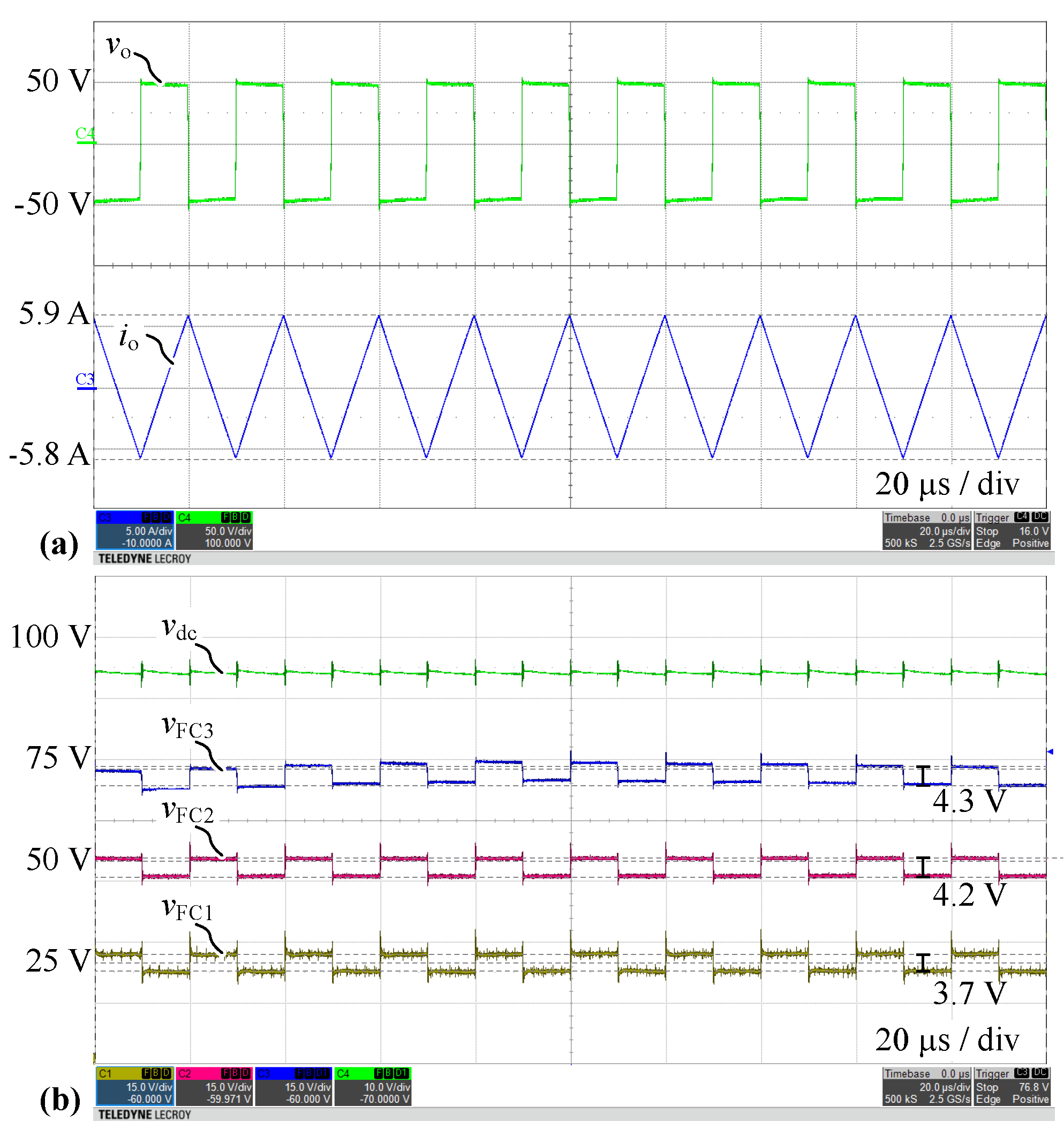
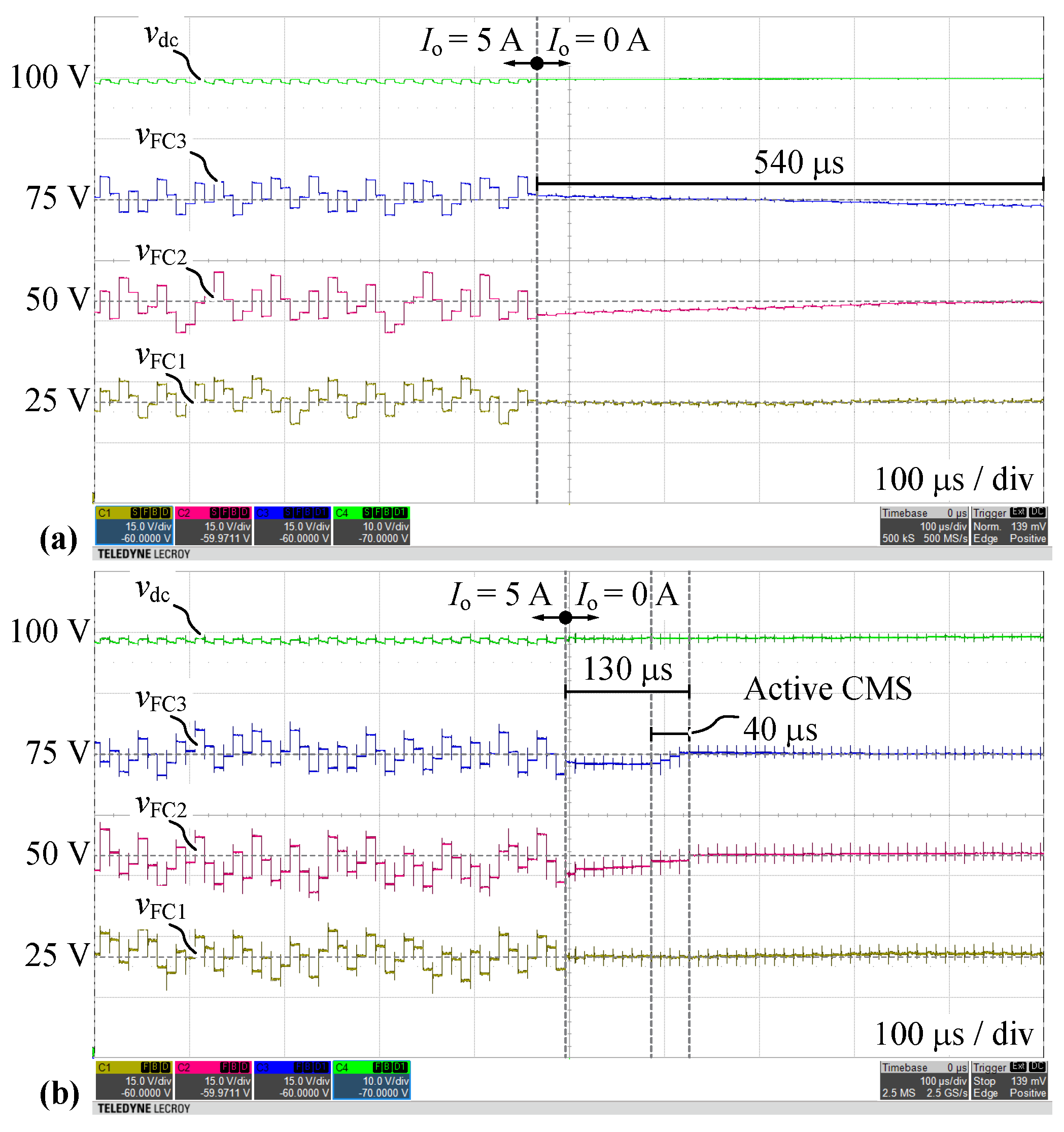
6.3.2. Balancing with Zero Output Current

Figure 20 compares no-load FC voltage balancing for OL and CL balancing during full load shedding ( I o = 5 A 0 A ) in a full DC-link configuration. Figure 20a shows the operation with resistive balancers and OL balancing, whereas Figure 20b illustrates the proposed CL controller concept employing CMS, cf. Section 4.2. Note the delay before CMS activation which is a consequence of the implemented hysteresis. Nevertheless, the CL controller achieves better dynamics as the steady-state is achieved after approx. 130 μs compared to appox. 540 μs settling time in case of resistive/OL balancing. It is noteworthy that the resistive balancers need to be selected considering the leakage currents of the switches and capacitors, therefore the time constant of the resistive balancing is determined by the circuitry and there are only limited tuning possibilities, especially if the losses in the balancing resistors must be limited. Furthermore, the resistive balancers are generating continuous losses, whereas in case of balancing with CMS, the zero-current hard-switching losses occur only during activation of CMS, i.e., several events at most over tens of switching transitions which leads to negligible average losses.

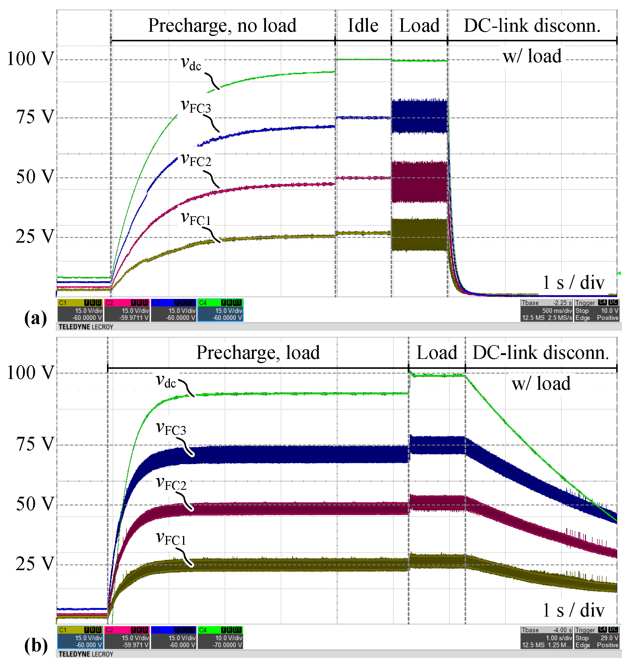
6.4. Start-Up and Shut-Down

In the last part of experimental validation we demonstrate voltage balancing during start-up and shut-down of the Q2L-5L-FCC. Note that in both experiments CL balancing is used.
Figure 21a presents measured waveforms in a full DC-link configuration with resistive balancers. The operation profile consists of the following intervals: A DC-link precharge via a resistor (disconnected load) → idle operation of Q2L-FCC after bridging the precharging resistor → connection of the load (nominal FC voltage ripple) → disconnection of the input supply and dissipation of the DC-link energy in the load. It can be noticed that the FC voltages are brought smoothly to and remain close to the their reference average values in the steady-state. Note that the jump in the capacitor’s voltage at the transition from precharge to idle interval is caused by the bridging of the precharging resistor. Furthermore, from the start of the idle interval the CL controller is active.
Figure 21b shows measured waveforms of a similar operation profile but in a split DC-link configuration without resistive balancers, however, in this case, the load is connected at all times. Again, it can be stated that the proposed CL balancing concept ensures balanced FC voltages and thus defined voltage levels on the switches in all operating modes of the Q2L-FCC.

7. Conclusions

This paper presents a new, comprehensive control concept for load-independent voltage balancing of flying capacitor converters (FCCs) operated in quasi-2-level mode (Q2L-FCC). This new and fully experimentally-verified concept ensures well-defined FC voltages and equal blocking voltages across the series-connected switches with and without load current flowing in the bridge-leg’s output terminal.
The proposed closed-loop voltage balancing control concept comprises two methods which are activated depending on the output current of the bridge-leg. In case of a non-zero output current, a first method of active cell voltage balancing involves a model predictive controller (MPC) that selects the most suitable sequence of FC cell commutations within one Q2L transition (1-step horizon) from all possible permutations by minimizing the predicted deviation from the reference values. On the other hand, when the output current is zero, a novel method to balance the FC voltages by means of cell multiple switching (CMS) is used. CMS utilizes the fact that during zero-current hard-switching of a switch, the commutation loop current leads to an exchange of charge (subtraction of charge in a cell’s input-side capacitor and addition of that charge to the output-side capacitor) which is equal to the charge stored in the switch’s parasitic capacitance. By adding additional switching actions during a Q2L transition, the FC voltages can be adjusted. Again, an MPC approach is utilized to select the optimum CMS sequence, however, using FC voltage reference tracking over a 6-step horizon.
The proposed voltage balancing control concept is thoroughly validated with a 5-level FCC half-bridge demonstrator for hard-switching and soft-switching output voltage transitions, during load transients, as well as for start-up and shut-down operation modes. The hardware experiments demonstrate an excellent average FC voltage tracking as well as symmetric cell voltages. More importantly, the results prove the validity of the proposed description of charge and voltage increments in FCs. The presented closed-loop cell voltage control concept, compared to open-loop (passive) balancing or active balancing directly controlling FC voltages, results in voltages across the switches that are close to the ideal values and optimum FC voltage ripples. The versatility of the proposed solution comes at the price of the required measurement circuitry to sense the FC voltages. In return, however, the proposed controller is computationally efficient and can be easily implemented in an FPGA, partially using offline-generated look-up tables.
Alternatively, the future research should focus on the FC voltages estimation from the switching sequence and the output voltage since the FC voltages combined with the DC-link voltage appear in the output voltage during the Q2L transitions, which would enable ‘sensor-less’ FC voltages balancing.
The proposed closed-loop voltage balancing turns the Q2L-FCC into a robust versatile half-bridge power semiconductor stage for various hard-switched and soft-switched applications such as AC-DC rectifiers and isolated DC-DC converters, where the system voltages exceed the voltage ratings of available power semiconductors.

Author Contributions

Conceptualization, P.C., P.P., T.G., F.K. and J.W.K.; methodology, P.C.; software, F.T.B., V.L.; validation, P.C., F.T.B., P.P. and J.H.; formal analysis, P.C., F.T.B., V.L. and F.K.; investigation, P.C. and J.H.; resources, J.W.K.; data curation, P.C.; writing—original draft preparation, P.C.; writing—review and editing, P.C., F.T.B., J.H. and J.W.K.; supervision, J.W.K.; project administration, J.W.K. All authors have read and agreed to the published version of the manuscript.

Funding

This research was funded by SCCER-FURIES.

Data Availability Statement

The data presented in this study are available on request from the corresponding author.

Acknowledgments

The authors are very much indebted to the Swiss Centre for Competence in Energy Research on the Future Swiss Electrical Infrastructure (SCCER-FURIES) for the support of the research in the area of Solid-State Transformer technology at ETH Zurich.

Conflicts of Interest

The authors declare no conflict of interest.

Abbreviations

The following abbreviations are used in this manuscript:
CMSCell multiple switching
FCFlying capacitor
FCCFlying capacitor converter
HSHard-switching
MPCModel predictive control
MSMixed sequences
Q2LQuasi-2-level
ZVSZero voltage switching
1 i , j Matrix of ones of dimensions i × j
C FC FC value
C Q , eq Charge equivalent output capacitance
dDuty cycle
Δ I pp Peak-to-peak output current ripple
Δ V FC Voltage increment on the FC
Δ V pp Peak-to-peak voltage ripple
Δ V CMS Voltage increment in CMS
Δ Q FC Charge increments in FC
i c Instantaneous FC current
i o Instantaneous output current
I o Average output current
I o , max Maximum peak output current
jNumber of FCs
JCost function
kDiscrete time step
NNumber of FCC voltage levels
nNumber of FCC cells ( n = N 1 )
N p Prediction horizon
S E Q Sequence of cell commutations
T t Transition time
T delay Delay time
T p Pulse time
T CMS CMS time
T s Switching period
v c Instantaneous FC voltage
v o Instantaneous output voltage
V dc DC-link voltage

Appendix A. CMS for Semiconductors of Various Voltage Classes

The proposed method for balancing the FC voltages without load current, i.e., cell multiple switching (CMS), relies on the charge stored in the output capacitances of the switches, cf. (12). Section 6.3.2 shows experimental validation for 150 V GaN eFETs (EPC2033) operated at a reduced (for safety reasons) V s = 25 V , cf. ➀ in Table A1. However, the question arises whether this result is representative also for higher voltages, and then for power semiconductors of different voltage classes.
Therefore, we consider the following semiconductors in Q2L-5L-FCC designs with typical ratings for the given device: 150 V GaN eFET (EPC2033), 1.7 kV SiC MOSFET (C2M0045170P) and 10 kV SiC MOSFET (QPM3-10000-0300), cf. Table A1. Figure A1 shows the absolute voltage increment per CMS event, cf. (12) as a function of the capacitance ratio k c = 2 C Q , eq / C FC . For a fixed delay time and a maximum output current, a higher allowed FC voltage ripple results in a lower FC capacitance requirement, and therefore, for a given switch voltage, in a better controllability (i.e., larger voltage increment per CMS event). Moreover, it can can be noticed that for the GaN eFETs operated at 25 V (for Δ V pp = 20 % , see Electronics 10 02414 i003), the value of Δ V CMS = 1.1 V corresponds to approx. half of the maximum increment when operated at 100 V ( 2.3 V ). This can be explained by the 4 × higher switch voltage but approx. factor of 2 lower C Q , eq in case of ➁ which indicates that the controllability at 100 V would be better for the same absolute value of voltage ripple which is discussed in detail in the following.
To assess CMS controllability, a relative voltage increment k V defined as ratio of Δ V CMS / Δ V pp is introduced. Since the value of the FCs is designed for a desired voltage ripple, the relative voltage increment is constant for the considered semiconductor and operating parameters, and the respective values are shown in Table A1. We use the same absolute voltage ripple in the experiments with the demonstrator at 25 V as for operation at 100 V , hence reducing the controllability ( 5.6 % vs. 11.5 % ), therefore the measurements represent the worst-case scenario. Finally, it can be seen that CMS events in case of 1.7 kV and 10 kV SiC MOSFETs provide even more controllability than Q2L-FCC with 150 V GaN eFETs.
Table A1. Parameters for CMS controllability analysis for semiconductors of various voltage classes for the considered relative peak-to-peak FC voltage ripple range Δ V pp = Δ V pp / V s [ 5 % , 20 % ] .
Param.150 V GaN
(EPC2033)
1.7 kV SiC
(C2M0045170P)
10 kV SiC
(QPM3-10000-0300)
V dc 100 V 400 V 4.4 kV 26.8 kV DC-link voltage
V s 25 V 100 V 1.1 kV 6.7 kV switch voltage
C oss , eq 1480 pF 760 pF 727 pF 200 pF charge eq. capacitance
I o , max 6.6 A 6.6 A 28 A 10.75 A max. output current
I o , ZVS 2.5 A 2.5 A 8 A 6 A min. output current w/ZVS
T delay 100 nF 100 nF 200 nF 1000 nF max. delay time
Relative controllability
k V = Δ V CMS Δ V pp 5.6 % 11.5 % 14.7 % 12.4 % relative CMS controllability
Δ V pp 5–20 V 1 5–20 V57–227 V0.33–1.33 kVpeak-to-peak volt. ripple
1 Note that in case ➀ in experiments a relative peak-to-peak FC voltage ripple of 80 % is used.
Figure A1. Absolute voltage increment per CMS event ( Δ V CMS ) for semiconductors of various voltage classes as functions of the capacitance ratio k c = 2 C Q , eq / C FC for the considered relative peak-to-peak FC voltage ripple range Δ V pp = Δ V pp / V s [ 5 % , 20 % ] .
Electronics 10 02414 g0a1

Appendix B. Discussion of Overload and Short-Circuit Operation

In case of excessive currents, i.e., overload or short-circuit currents (e.g., 10 × higher than nominal) at the output of Q2L-operated half-bridge, there is a risk of overcharging the FCs. Moreover, unequal voltage sharing among the switches could ultimately lead to their destruction. However, from the Q2L operation description in Section 2 we know that a fault needs to be present during the switching transition, therefore in a relatively short interval compared to the dynamics of the system ( d i / d t ), to create hazardous conditions for the capacitors and their voltages. To mitigate the eventual overvoltage conditions, we propose to set an ultra-short delay time T delay = T sh (with T sh in the range of rise/falling switching times of the semiconductors, as hard-switching is expected), which is applied in the Q2L switching transitions following an overcurrent detection. If the gate drivers are equipped with (ultra)-fast overcurrent detection, the fault can be cleared within 100 ns for LV GaN switches [43] and within 200 ns for MV SiC MOSFETs [44]. Thus, in the worst-case scenario, only a single Q2L transition will be impacted by excessive currents. In this regard, a correctly dimensioned T sh should be sufficient to avoid harmful voltage deviations.
Furthermore, in case of some MOSFETs, e.g., 10 kV SiC MOSFETS, due to the excessively high drain current in the conducting switches the so-called self turn-off occurs, caused by the voltage drop across the source inductance [44]. This phenomenon effectively leads to the simultaneous switching of series connected MOSFETs as in a 2L bridge-leg. As a result, the commutations of the individual cells overlap, leading to a continuous output voltage change instead of a staggered transition. Hence, the charge increments of the FCs are negligible and it can be concluded that under such conditions the operation of Q2L-FCC is not critical. Further investigations are out of the scope of this paper, but should be performed in the course of further analysis of the proposed FC voltage balancing concept.

References

  1. Hafez, B.; Krishnamoorthy, H.S.; Enjeti, P.; Ahmed, S.; Pitel, I.J. Medium Voltage Power Distribution Architecture with Medium Frequency Isolation Transformer for Data Centers. In Proceedings of the 2014 IEEE Applied Power Electronics Conference and Exposition-APEC 2014, Fort Worth, TX, USA, 16–20 March 2014. [Google Scholar]
  2. Rothmund, D.; Guillod, T.; Bortis, D.; Kolar, J.W. 99% Efficient 10 kV SiC-Based 7 kV/400 V DC-Transformer for Future Data Centers. IEEE Trans. Emerg. Sel. Top. Power Electron. 2019, 7, 753–767. [Google Scholar] [CrossRef]
  3. Li, Z.; Hsieh, Y.H.; Li, Q.; Lee, F.C.; Ahmed, M.H. High-Frequency Transformer Design with High-Voltage Insulation for Modular Power Conversion from Medium-Voltage AC to 400-V DC. In Proceedings of the IEEE Energy Conversion Congress and Exposition (ECCE), Detroit, MI, USA, 11–15 October 2020. [Google Scholar]
  4. Zhao, C.; Hsieh, Y.H.; Lee, F.C.; Li, Q. Design and Analysis of a High-Frequency CLLC Resonant Converter with Medium Voltage Insulation for Solid-State-Transformer. In Proceedings of the 2021 IEEE Applied Power Electronics Conference and Exposition (APEC), Phoenix, AZ, USA, 14–17 June 2021. [Google Scholar]
  5. Srdic, S.; Lukic, S. Toward Extreme Fast Charging: Challenges and Opportunities in Directly Connecting to Medium-Voltage Line. IEEE Electrif. Mag. 2019, 7, 22–31. [Google Scholar] [CrossRef]
  6. Tu, H.; Feng, H.; Srdic, S.; Lukic, S. Extreme Fast Charging of Electric Vehicles: A Technology Overview. IEEE Trans. Transp. Electrif. 2019, 5, 861–878. [Google Scholar] [CrossRef]
  7. Delta Electronics. High-Efficiency, Medium-Voltage-Input, Solid-State-Transformer-Based 400-kW/1000-V/400-A Extreme Fast Charger for Electric Vehicles. Available online: https://www.energy.gov/ (accessed on 30 August 2021).
  8. Liang, X.; Srdic, S.; Won, J.; Aponte, E.; Booth, K.; Lukic, S. A 12.47 kV Medium Voltage Input 350 kW EV Fast Charger using 10 kV SiC MOSFET. In Proceedings of the 2019 IEEE Applied Power Electronics Conference and Exposition (APEC), Anaheim, CA, USA, 17–21 March 2019. [Google Scholar]
  9. Zhao, S.; Li, Q.; Lee, F.C.; Li, B. High-Frequency Transformer Design for Modular Power Conversion from Medium-Voltage AC to 400 VDC. IEEE Trans. Power Electron. 2018, 33, 7545–7557. [Google Scholar] [CrossRef]
  10. Huber, J.E.; Kolar, J.W. Applicability of Solid-State Transformers in Today’s and Future Distribution Grids. IEEE Trans. Smart Grid 2019, 10, 317–326. [Google Scholar] [CrossRef]
  11. Cree/Wolfspeed. Medium Voltage SiC R&D Update 2016. Available online: https://www.wolfspeed.com/ (accessed on 30 August 2021).
  12. She, X.; Huang, A.Q.; Lucia, O.; Ozpineci, B. Review of Silicon Carbide Power Devices and Their Applications. IEEE Trans. Ind. Electron. 2017, 64, 8193–8205. [Google Scholar] [CrossRef]
  13. Kicin, S.; Burkart, R.; Loisy, J.Y.; Canales, F.; Nawaz, M.; Stampf, G.; Morin, P.; Keller, T. Ultra-Fast Switching 3.3 kV SiC High-Power Module. In Proceedings of the International Exhibition and Conference for Power Electronics, Intelligent Motion, Renewable Energy and Energy Management (PCIM Europe), Nuremberg, Germany, 7–8 July 2020. [Google Scholar]
  14. ABB Power Grids. Power Semiconductors. Available online: https://library.abb.com/ (accessed on 30 August 2021).
  15. Mainali, K.; Tripathi, A.; Madhusoodhanan, S.; Kadavelugu, A.; Patel, D.; Hazra, S.; Hatua, K.; Bhattacharya, S. A Transformerless Intelligent Power Substation: A Three-Phase SST Enabled by a 15-kV SiC IGBT. IEEE Power Electron. Mag. 2015, 2, 31–43. [Google Scholar] [CrossRef]
  16. PowerAmerica. Annual Report: Through Advances in Wide Bandgap Power Electronics. Available online: https://poweramericainstitute.org/ (accessed on 30 August 2021).
  17. Vechalapu, K.; Negi, A.; Bhattacharya, S. Comparative Performance Evaluation of Series Connected 15 kV SiC IGBT Devices and 15 kV SiC MOSFET Devices for MV Power Conversion Systems. In Proceedings of the 2016 IEEE Energy Conversion Congress and Exposition (ECCE), Milwaukee, WI, USA, 18–22 September 2016. [Google Scholar]
  18. Rodriguez, J.; Bernet, S.; Wu, B.; Pontt, J.O.; Kouro, S. Multilevel Voltage-Source-Converter Topologies for Industrial Medium-Voltage Drives. IEEE Trans. Ind. Electron. 2007, 54, 2930–2945. [Google Scholar] [CrossRef]
  19. Biela, J.; Aggeler, D.; Bortis, D.; Kolar, J.W. Balancing Circuit for a 5-kV/50-ns Pulsed-Power Switch Based on SiC-JFET Super Cascode. IEEE Trans. Plasma Sci. 2012, 40, 2554–2560. [Google Scholar] [CrossRef]
  20. Li, Z.; Bhalla, A. USCi SiC JFET Cascode and Super Cascode Technologies. In Proceedings of the International Exhibition and Conference for Power Electronics, Intelligent Motion, Renewable Energy and Energy Management (PCIM Asia), Shanghai, China, 26–28 June 2018. [Google Scholar]
  21. Gowaid, I.A.; Adam, G.P.; Ahmed, S.; Holliday, D.; Williams, B.W. Analysis and Design of a Modular Multilevel Converter with Trapezoidal Modulation for Medium and High Voltage DC-DC Transformers. IEEE Trans. Power Electron. 2015, 30, 5439–5457. [Google Scholar] [CrossRef] [Green Version]
  22. Aeloiza, D.; Canales, F.; Burgos, R. Power Converter Having Integrated Capacitor-Blocked Transistor Cells. U.S. Patent 9525348B1, 20 December 2016. [Google Scholar]
  23. Gowaid, I.A.; Adam, G.P.; Massoud, A.M.; Ahmed, S.; Holliday, D.; Williams, B.W. Quasi Two-Level Operation of Modular Multilevel Converter for Use in a High-Power DC Transformer with DC Fault Isolation Capability. IEEE Trans. Power Electron. 2015, 30, 108–123. [Google Scholar] [CrossRef] [Green Version]
  24. Milovanovic, S.; Dujic, D. Comprehensive Analysis and Design of a Quasi Two-Level Converter Leg. CPSS Trans. Power Electron. Appl. 2019, 4, 181–196. [Google Scholar] [CrossRef]
  25. Jiao, D.; Huang, Q.; Huang, A.Q. Evaluation of Medium Voltage SiC Flying Capacitor Converter and Modular Multilevel Converter. In Proceedings of the IEEE Energy Conversion Congress and Exposition (ECCE USA), Detroit, MI, USA, 11–15 October 2020. [Google Scholar]
  26. Fazel, S.S.; Bernet, S.; Krug, D.; Jalili, K. Design and Comparison of 4-kV Neutral-Point-Clamped, Flying-Capacitor, and Series-Connected H-Bridge Multilevel Converters. IEEE Trans. Ind. Appl. 2007, 43, 1032–1040. [Google Scholar] [CrossRef]
  27. Papamanolis, P.; Neumayr, D.; Kolar, J.W. Behavior of the Flying Capacitor Converter under Critical Operating Conditions. In Proceedings of the IEEE International Symposium on Industrial Electronics (ISIE), Edinburgh, UK, 19–21 June 2017. [Google Scholar]
  28. Schweizer, M.; Soeiro, T.B. Heatsink-Less Quasi 3-Level Flying Capacitor Inverter Based on Low Voltage SMD MOSFETs. In Proceedings of the IEEE European Conference on Power Electronics and Applications (EPE), Warsaw, Poland, 11–14 September 2017. [Google Scholar]
  29. Czyz, P.; Papamanolis, P.; Guillod, T.; Krismer, F.; Kolar, J.W. New 40kV/300kVA Quasi-2-Level Operated 5-Level Flying Capacitor SiC “Super-Switch” IPM. In Proceedings of the IEEE International Power Electronics Conference (ECCE Asia), Busan, Korea, 27–30 May 2019. [Google Scholar]
  30. Kucka, J.; Lin, S.; Friebe, J.; Mertens, A. Quasi-Two-Level PWM-Operated Modular Multilevel Converter with Non-Linear Branch Inductors. IEEE Trans. Power Electron. 2019, 36, 7600–7611. [Google Scholar] [CrossRef]
  31. Gierschner, S.; Hein, Y.; Gierschner, M.; Sajid, A.; Eckel, H.G. Quasi-Two-Level Operation of a Five-Level Flying-Capacitor Converter. In Proceedings of the IEEE European Conference on Power Electronics and Applications (EPE), Genova, Italy, 3–5 September 2019. [Google Scholar]
  32. Mersche, S.; Bernet, D.; Hiller, M. Quasi-Two-Level Flying-Capacitor-Converter for Medium Voltage Grid Applications. In Proceedings of the IEEE Energy Conversion Congress and Exposition (ECCE USA), Baltimore, MD, USA, 29 September–3 October 2019. [Google Scholar]
  33. Tcai, A.; Wijekoon, T.; Liserre, M. Evaluation of Flying Capacitor Quasi 2-level Modulation for MV Applications. In Proceedings of the International Exhibition and Conference for Power Electronics, Intelligent Motion, Renewable Energy and Energy Management (PCIM Europe), Online, 3–7 May 2021. [Google Scholar]
  34. Lu, C.; Hu, W.; Wu, H.; Lee, F.C. Quasi-Two-Level Bridgeless PFC Rectifier for Cascaded Unidirectional Solid State Transformer. IEEE Trans. Power Electron. 2021, 36, 12033–12044. [Google Scholar] [CrossRef]
  35. Fabiani, D.; Montanari, G.C.; Contin, A. Aging Acceleration of Insulating Materials for Electrical Machine Windings Supplied by PWM in the Presence and in the Absence of Partial Discharges. In Proceedings of the IEEE Conference on Solid Dielectrics (ICSD), Eindhoven, The Netherlands, 25–29 June 2001. [Google Scholar]
  36. Wang, P.; Montanari, G.C.; Cavallini, A. Partial Discharge Phenomenology and Induced Aging Behavior in Rotating Machines Controlled by Power Electronics. IEEE Trans. Ind. Electron. 2014, 61, 7105–7112. [Google Scholar] [CrossRef]
  37. Guillod, T.; Faerber, R.; Rothmund, D.; Krismer, F.; Franck, C.M.; Kolar, J.W. Dielectric Losses in Dry-Type Insulation of Medium-Voltage Power Electronic Converters. IEEE Trans. Emerg. Sel. Top. Power Electron. 2020, 8, 2716–2732. [Google Scholar] [CrossRef] [Green Version]
  38. Hu, A.; Biela, J. Evaluation of the Imax-fsw-dv/dt Trade-off of High Voltage SiC MOSFETs Based on an Analytical Switching Loss Model. In Proceedings of the IEEE European Conference on Power Electronics and Applications (EPE), Lyon, France, 7–11 September 2020. [Google Scholar]
  39. Wilkinson, R.H.; Meynard, T.A.; du Toit Mouton, H. Natural Balance of Multicell Converters: The General Case. IEEE Trans. Power Electron. 2006, 21, 1658–1666. [Google Scholar] [CrossRef]
  40. Czyz, P.; Papamanolis, P.; Lazarevic, V.; Guillod, T.; Krismer, F.; Kolar, J.W. Voltage Source Converter Configured to Transition Between at Least Two Voltage Levels. Patent SE 2051394-1, 11 February 2020. [Google Scholar]
  41. Geyer, T. Model Predictive Control of High Power Converters and Industrial Drives; John Wiley & Sons: Hoboken, NJ, USA, 2017. [Google Scholar]
  42. Antoniewicz, K.; Jasinski, M.; Kazmierkowski, M.P.; Malinowski, M. Model Predictive Control for Three-Level Four-Leg Flying Capacitor Converter Operating as Shunt Active Power Filter. IEEE Trans. Ind. Electron. 2016, 63, 5255–5262. [Google Scholar]
  43. Acuna, J.; Walter, J.; Kallfass, I. Very Fast Short Circuit Protection for Gallium-Nitride Power Transistors Based on Printed Circuit Board Integrated Current Sensor. In Proceedings of the IEEE European Conference on Power Electronics and Applications (EPE), Riga, Latvia, 17–21 September 2018. [Google Scholar]
  44. Rothmund, D.; Bortis, D.; Kolar, J.W. Highly Compact Isolated Gate Driver with Ultrafast Overcurrent Protection for 10 kV SiC MOSFETs. CPSS Trans. Power Electron. Appl. 2018, 3, 278–291. [Google Scholar] [CrossRef]
Figure 1. (a) Considered 5-level flying capacitor converter (5L-FCC) HB with two alternative load/DC-link connections (➀ and ➁). Corresponding exemplary output waveforms and characteristic staggered Q2L transitions of the output voltage v o for: (b) Symmetric output current i o (ZVS transitions), (c) asymmetric output current i o (ZVS & HS transitions).
Electronics 10 02414 g001
Figure 2. Simulation results for Q2L operation of the 5L-FCC: (a) Switching states of a FCC HB with constant positive output current ( I o , max ) during a Q2L switching transition with negative slope of v o , resulting in ZVS. (b) Corresponding time intervals and simulated waveforms of output current ( i o ) and output voltage ( v o ), FC voltages ( v FC { 1 , 2 , 3 } ) and currents ( i FC { 1 , 2 , 3 } ), and MOSFET gating signals. (c) Time intervals and simulated waveforms for the HS case with positive slope of v o and constant output current.
Electronics 10 02414 g002
Figure 3. Simulation results for Q2L operation of the 5L-FCC with constant positive output current ( I o ) during the switching transition with negative slope of v o , exemplifying the effect of a non-consecutive sequence S E Q 1324 : Charging of FC1 and FC3, discharging of FC2.
Electronics 10 02414 g003
Figure 4. Simulation results for the 5L-FCC in configuration ➀ with zero output current during the Q2L transition with negative slope of v o : Zero net charge increments of the FCs result.
Electronics 10 02414 g004
Figure 5. Simulation results for the 5L-FCC in configuration ➀ with zero output current during the Q2L transition with negative slope of v o : Note the single cell multiple switching event of cell 3. A delay T delay and a pulse time T p = 0.5 T delay are used. Note that the same T delay , however a different time base are used compared to Figure 4.
Electronics 10 02414 g005
Figure 6. (a) Block diagram of an FCC HB with Q2L voltage balancing controller and modulator. Note that the output quantity (e.g., load current) controller is not in this paper’s scope and hence we consider an exemplary fixed duty cycle of d = 50 % . (b) Control block diagram of the proposed load-independent Q2L voltage balancing controller.
Electronics 10 02414 g006
Figure 7. Detailed state machine of the modulator shown in Figure 6a. Cell[i] stores the two gate signals of the two switches of cell i; T FPGA denotes the FPGA clock period. Note that T delay and T p are shown as scalars for simplicity (i.e., all commutations within one Q2L transition use the same values), but it would be possible to specify vectors indexed by ind such that individual values for each commutation could be used.
Electronics 10 02414 g007
Figure 8. (a) Simulation results illustrating the PWM carrier, output voltage switching transition reference V o and main waveforms. Note that the ADCs are triggered shortly before the switching transition. (b) Gate signals, output voltage and current waveforms at discrete time step k including the delay times introduced by the ADC conversion and FPGA computation.
Electronics 10 02414 g008
Figure 9. Schematic (cf. also Figure 1) of the 5L-FCC used in experiments with two configurations: ➀ Split DC-link at the input and inductive load connected to the DC-link mid-point to obtain symmetrical currents; ➁ full DC-link at the input and LC filter with resistive load in the output to achieve asymmetrical currents.
Electronics 10 02414 g009
Figure 10. Photos of the realized 5L-FCC HB demonstrator: (a) General assembly, (b) power board and detail view of the switching cell PCBs.
Electronics 10 02414 g010
Figure 11. Measured waveforms for Q2L-5L-FCC in configuration ➀ with negative output current ( I o = 5.9 A ) during the switching transition with positive slope of v o , which results in a ZVS transition: (a) Output voltage v o and current i o , (b) DC-link capacitor voltage v dc and FC voltages v FC { 1 , 2 , 3 } . A delay time of T delay = 100 ns is used.
Electronics 10 02414 g011
Figure 12. Measured waveforms for Q2L-5L-FCC in configuration ➁ with positive output current ( i o = 2.9 A ) during the switching transition with positive slope of v o , which results in a HS transition: (a) Output voltage v o and current i o , (b) DC-link capacitor voltage v dc and FC voltages v FC { 1 , 2 , 3 } . A delay time of T delay = 50 ns is used.
Electronics 10 02414 g012
Figure 13. Measured waveforms for Q2L-5L-FCC in configuration ➁ with zero output current ( I o = 0 A ) during the switching transition with negative slope of v o and CMS sequence S E Q 1 ( 11 ) 234 (events in cells ‘1000’): (a) Output voltage v o and current i o , (b) DC-link capacitor voltage v dc and FC voltages v FC { 1 , 2 , 3 } . Delay times and pulse time T delay = T p = 50 ns are used.
Electronics 10 02414 g013
Figure 14. Measured waveforms for Q2L-5L-FCC in configuration ➀ with OL balancing and triangular current ( I o , max = 7.0 A , I o , min = 5.8 A ): (a) Output voltage v o and current i o , (b) DC-link capacitor voltage v dc and FC voltages v FC { 1 , 2 , 3 } . A delay time T delay = 100 ns is used.
Electronics 10 02414 g014
Figure 15. Measured waveforms for Q2L-5L-FCC in configuration ➁ with OL balancing during a negative load step from 100% to 67% of the nominal load ( I o = 4.6 A 3.0 A , Δ I pp = 4 A ): (a) Output voltage v o and current i o , (b) DC-link capacitor voltage ( v dc ) and FC voltages v FC { 1 , 2 , 3 } . A delay time T delay = 100 ns is used.
Electronics 10 02414 g015
Figure 16. Measured waveforms for Q2L-5L-FCC in configuration ➀ with CL balancing and triangular current ( I o , max = 5.9 A , I o , min = 5.8 A ): (a) Output voltage v o and current i o , (b) DC-link capacitor voltage v dc and FC voltages v FC { 1 , 2 , 3 } . A delay time T delay = 50 ns is used.
Electronics 10 02414 g016
Figure 17. Measured waveforms for Q2L-5L-FCC in configuration ➁ with CL balancing during a negative load step from 100% to 67% of the nominal load ( I o = 4.6 A 3.0 A , Δ I pp = 4 A ): (a) Output voltage v o and current i o , (b) DC-link capacitor voltage v dc and FC voltages v FC { 1 , 2 , 3 } . Delay times T delay = { 50 , 100 } ns are used.
Electronics 10 02414 g017
Figure 18. Measured waveforms for Q2L-5L-FCC in configuration ➁ with transition from OL ( T delay = 100 ns ) to CL ( T delay = { 50 , 100 } ns ) balancing with nominal output current ( I o = 4.6 A ): (a) Output voltage v o and current i o , (b) DC-link capacitor voltage v dc and FC voltages v FC { 1 , 2 , 3 } .
Electronics 10 02414 g018
Figure 19. Cell voltages V cell , cf. (31), corresponding to the experiment from Figure 18 (transition from OL to CL balancing with nominal current). Data computed and filtered from oscilloscope waveforms. Note that the ideal cell voltages should be equal to 100 V/4 = 25 V.
Electronics 10 02414 g019
Figure 20. Comparison of measured waveforms (DC-link capacitor voltage v dc , FC voltages v FC { 1 , 2 , 3 } ) for Q2L-5L-FCC in a full DC-link configuration during load disconnection ( I o = 5 A 0 A ): (a) OL with resistive balancers; (b) CL balancing with CMS. Delay times T delay = T p = 50 ns are used.
Electronics 10 02414 g020
Figure 21. Measured waveforms (DC-link capacitor voltage v dc , FC voltages v FC { 1 , 2 , 3 } ) for start-up (precharging) and shut-down of Q2L-5L-FCC: (a) Full DC-link configuration with resistive balancers (precharge → idle → nominal load → DC-link voltage disconnection under load). (b) Split DC-link configuration without resistive balancers (precharge under load → nominal load → DC-link voltage disconnection under load). Note the different time bases due to the different DC-link capacitance values.
Electronics 10 02414 g021
Table 1. Effect of all sequences available ( S CL ) for Q2L-5L-FCC on FC charge increments in the function of delay times for Q2L ZVS transition (for HS transition, the same value but opposite signs apply): (+1) charge, (−1) discharge, (0) no effect. Scaling the values with the respective T delay { n } and I o , max gives the charge increment values. Note that the table is simplified and values for S E Q 3 xxx and S E Q 4 xxx are obtained by using symmetry and multiplying the respective values by (−1).
Electronics 10 02414 i001FC1FC2FC3
Sequence T delay 1 T delay 2 T delay 3 T delay 4 T delay 1 T delay 2 T delay 3 T delay 4 T delay 1 T delay 2 T delay 3 T delay 4
S E Q 1234 +10000+10000+10 S E Q 4321
S E Q 1243 +10000+10+1000−1 S E Q 4312
S E Q 1324 +10+1000−100+1+10 S E Q 4231
S E Q 1342 +10+1+100−1−100+10 S E Q 4213
S E Q 1423 +100+10+1000−10−1 S E Q 4132
S E Q 1432 +10+1+100−10000−1 S E Q 4123
S E Q 2134 0−100+1+10000+10 S E Q 3421
S E Q 2143 0−100+1+10+1000−1 S E Q 3412
S E Q 2314 0−1−100+100+10+10 S E Q 3241
S E Q 2341 0−1−1−10+10000+10 S E Q 3214
S E Q 2413 0−10−1+1+10+1−100−1 S E Q 3142
S E Q 2431 0−1−1−10+10+1000−1 S E Q 3124
T delay 4 T delay 3 T delay 2 T delay 1 T delay 4 T delay 3 T delay 2 T delay 1 T delay 4 T delay 3 T delay 2 T delay 1 Sequence
FC3FC2FC1 Electronics 10 02414 i002
Table 2. Effect on charge increments of the FCs in dependence of different CMS events/sequences: (+1) charge, (−1) discharge, (0) no effect. Scaling the values by 2 Δ Q S gives the charge increment values.
CMS EventsCMS seq. Δ Q FC 1 Δ Q FC 2 Δ Q FC 3
0001 S E Q 1234 ( 44 ) 00+1
0010 S E Q 123 ( 33 ) 4 0+1−1
0100 S E Q 12 ( 22 ) 34 +1−10
1000 S E Q 1 ( 11 ) 234 −100
0011 S E Q 123 ( 33 ) 4 ( 44 ) 0+10
1100 S E Q 1 ( 11 ) 2 ( 22 ) 34 0−10
Table 3. Specifications and control parameters of the Q2L-5L-FCC proof-of-concept demonstrator.
V dc 100 VDC-link voltage
I o , max 6.6 Aoutput current maximum
f s 50 kHzswitching frequency
d50%duty cycle
Flying capacitors
C FC 66 nFCAA572C0G3A663J640LH
Δ V pp , max 20 Vmax. peak-to-peak volt. ripple
Semiconductors
S150 V/7 mGaN eFET EPC2033
C oss , eq 760 pFcharge eq. capacitance
Control parameters
T t , max 400 nsmax. transition time
T min 50 nsmin. delay time
T max 100 nsmax. delay time
T p 50 nspulse time
Publisher’s Note: MDPI stays neutral with regard to jurisdictional claims in published maps and institutional affiliations.

