Article

An 8-bit Radix-4 Non-Volatile Parallel Multiplier

1
College of Micro-Nano Electronics, Zhejiang University, Hangzhou 310027, China
2
Zhejiang Lab, Hangzhou 311101, China
3
College of Information Science & Electronic Engineering, Zhejiang University, Hangzhou 310027, China
4
School of Medicine, The Second Affiliated Hospital of Zhejiang University, Hangzhou 310027, China
*
Authors to whom correspondence should be addressed.
These authors contributed equally to this work.
Electronics 2021, 10(19), 2358; https://doi.org/10.3390/electronics10192358
Submission received: 31 July 2021 / Revised: 8 September 2021 / Accepted: 10 September 2021 / Published: 27 September 2021
(This article belongs to the Special Issue Advanced Analog Circuits for Emerging Applications)

Abstract

:
The data movement between the processing and storage units has been one of the most critical issues in modern computer systems. The emerging Resistive Random Access Memory (RRAM) technology has drawn tremendous attention due to its non-volatile ability and the potential in computation application. These properties make them a perfect choice for application in modern computing systems. In this paper, an 8-bit radix-4 non-volatile parallel multiplier is proposed, with improved computational capabilities. The corresponding booth encoding scheme, read-out circuit, simplified Wallace tree, and Manchester carry chain are presented, which help to short the delay of the proposed multiplier. While the presence of RRAM save computational time and overall power as multiplicand is stored beforehand. The area of the proposed non-volatile multiplier is reduced with improved computing speed. The proposed multiplier has an area of 785.2 μ m 2 with Generic Processing Design Kit 45 nm process. The simulation results show that the proposed multiplier structure has a low computing power at 161.19 μ W and a short delay of 0.83 ns with 1.2 V supply voltage. Comparative analyses are performed to demonstrate the effectiveness of the proposed multiplier design. Compared with conventional booth multipliers, the proposed multiplier structure reduces the energy and delay by more than 70% and 19%, respectively.

1. Introduction

In the past decade, oceans of data need to transfer and process in the big data era due to advancements in the fields of cloud computing, the Internet of Things (IoT), machine learning, and image processing. These technologies require both high data transfer rates and processing speeds. However, the modern computing systems are confined by data transfer rates in the bus [1]. Conventional computing architectures was not able to satisfy high computing demands with low computing energy requirements due to the segregated computing and storage units [2]. For instance, Von Neumann architecture carries out processing and the storing operation in the central processing unit (CPU) and memory, respectively [3]. These operations require the transfer of data elements between CPU and memory, thus limiting the overall computational speed. The phenomenon is known as the Von Neumann bottleneck [4,5]. A large number of studies have been conducted to address this problem. Recent research has shown that all Boolean operations can be implemented using non-volatile memory-based computing systems [6]. These computing systems integrate the non-volatile memory and computing capabilities in the same physical location to increase the computing speed.
The multipliers and adders are critical building blocks of modern computer system as virtually every arithmetic calculation involve a addition and multiplication. These units become even more significant due to its widespread utilization in computationally-heavy applications such as machine learning and the IoT. There are several different adder and multiplier designs reported in the literature [7,8,9,10]. The multiplier circuit can be classified based on its logic used as either serial or parallel multiplier [11]. Serial multipliers generate partial product in a sequential way and add new generated partial product to accumulated sum to get the product. Serial multiplier has small area and simple design for this reason they are still used in some application where time delay is not important factor. In array multipliers partial products are generated in parallel way. The array multiplier structure is simple and easy to expand. They have small area and easier design but the time delay is still higher [12]. Wallace tree multiplier is another type of multiplier structure which is faster compared with array multipliers. However, Wallace tree design is more complex and hard to implement. Booth multiplier is another type fast multiplier with low area and low power. Booth multiplier can be used in different 26 modes, i.e., radix-2, radix-4, radix-8, etc. Modified booth multiplier is used to avoid variable size of partial product generated [13]. The comparison of these multiplier designs is present in Table 1. This scarce presence of multipliers in the literature is remarkable since multiplication is among the most predominant functions of arithmetic logical units (ALUs).
In this paper, a non-volatile parallel multiplier design based on Resistive Random Access Memory (RRAM) is proposed with improved computational capabilities. Only a few examples are being reported to showcase the effectiveness of implementing non-volatile memory-based multiplier circuit designs to complex computing tasks [15,16]. In this paper, we have proposed an RRAM-based non-volatile multiplier design, which is suitable for low power application with less delay. We chose the RRAM in our multiplier design due to its potential in computation application utilizing smaller cell dimension, faster-switching speed, low I/V demands for read-write operation, and high OFF/ON resistance ratio [17]. In addition, it has higher reliability, data retention, and cycle endurance [18,19,20,21]. These characteristics make it a superior option for in-memory computing. Our design significantly improves the computational speed and reduces power consumption. Specifically, four partial products of 8 × 8 radix-4 booth encoding are formulated and connected sequentially to construct a multiplier. Results are obtained using a new Wallace tree structure containing only two stage. Fewer stages in our design make it faster than the conventional multipliers. The proposed 8-bit radix-4 non-volatile parallel multiplier has higher density compared to the conventional multiplier. The proposed multiplier circuit stores the multiplicator beforehand which makes it considerably faster by shortening the overall computational time. Furthermore, the multiplier is designed using RRAM which enables zero standby power consumption. The simulation results show that the proposed multiplier has better performance in terms of delay, power, and power delay production (PDP). The proposed multiplier has 70% less PDP, 63% lower power consumption, and 19% less delay, than the radix-4 booth multilevel resistance cell switching multiplier design.
The rest of the paper is structured as follows: Section 2 is the related work of conventional and nonvolatile multipliers, Section 3 provides the detailed description of the proposed 8-bit non-volatile radix-4 booth multiplier, Section 4 provides the simulation results and corresponding comparison. Finally, the conclusion is drawn in Section 5.

2. Background and Related Work

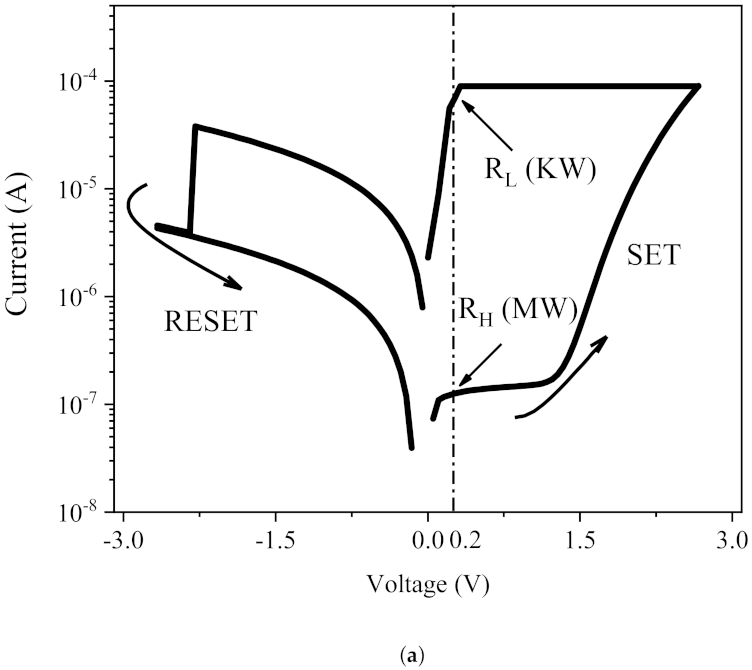
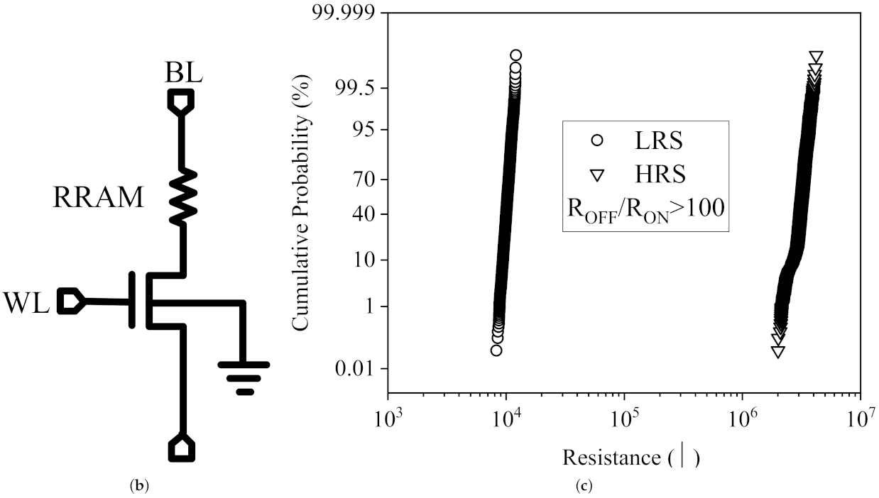
2.1. Resistive Non-Volatile Memory

The emerging Non-Volatile Memory (NVM) technologies provide quality hardware architecture due to its instant power-on speed, CMOS compatibility, high density [22,23], and standby power free [24]. To build up the non-volatile multiplier using NVMs, the full adder [25], flip-flop [26], and other basic arithmetic logic circuits are the most critical steps in constructing an in-memory computing system. The NVM technology is emerging with variety of representative candidates such as RRAM, Ferroelectric Random Access Memory (FeRAM), Phase Change Memory (PCM), and Magnetic Random Access Memory (MRAM) [27].
The development of crossbar memory structures based on RRAM technology may result in feasible and innovative solutions to effective non-volatile multipliers [19,20]. Among different types of NVMs, RRAM has shown great potential in the in-memory applications due to its merits such as nanometers cell dimension [18,28,29], nanoseconds switching speed [19,30,31], and microampere of read-write current with a low operation voltage [20,32,33]. Furthermore, it has a high OFF/ON resistance ratio [17,34,35] and good reliability, including data retention and cycle endurance [21,36,37]. Therefore, RRAM is chosen for this design to implement an 8-bit radix-4 non-volatile logic. Over the last decade, some non-volatile multipliers circuits based on innovative devices and circuits have been proposed. For instance, Wang et al. have proposed an implementation method with functionally complete Boolean logic incorporated in the 1T1R RRAM structure [38]. The method has low computation complexity and compatible with existing integration process of CMOS transistor. Further, in the NVM-based multiplier the power and computation time can be reduced without changing computing algorithm. However, technical solutions are still lacking for implementation of complex computing tasks like multiplication.
The RRAM has two terminals, the top electrode (TE) and the bottom electrode (BE). In the middle of these two electrodes, the generation and recombination of the oxygen vacancies in the oxide layer with applied positive/negative voltage, playing a significant role in resistance transformation. In the model of [39], the RRAM scheme is simplified to a single Conductive Filament (CF) in one dimension. Gap distance (g), a variable defined as the average distance between the TE and tip of the CF, is used to measure the RRAM resistance. According to electron tunneling conduction, the RRAM resistance can exponentially increase with g. Furthermore, the authors [39] also provides the nonlinear relationship between resistance and applied voltage (V) as follows:
I = I 0 e x p ( g g 0 ) s i n h ( V V 0 )
where I 0 , g 0 and V 0 are I–V fitting parameters. The gap growth/dissolution velocity can be expressed by the following equations:
d g d t = v 0 [ e x p ( q E a g k T ) e x p ( γ a 0 L q V k T ) e x p ( q E a r k T ) e x p ( γ a 0 L q V k T ) ]
γ = γ 0 β ( g g 1 ) 3
g ( t + d t ) = g ( t ) + d g
where k , q , a 0 , E a g , E a r , L are Boltzmann constant, elementary unit charge, atomic hopping distance, the activation energy for vacancy generation, the activation energy for vacancy recombination, and oxide thickness, respectively. v 0 , γ 0 , β are gap dynamics fitting parameters. γ , T are local field enhancement factors and temperature, respectively.
Thus, a positive SET voltage is given to RRAM for the generation of oxygen vacancies and oxygen ions at the tip of the CF. The CF layer will grow along with decrease in the gap distance, which switches the RRAM from high resistance state (HRS) to low resistance state (LRS). Similarly, the reverse transition is called RESET process. This mechanism of RRAM implements a logic storage function.
The RRAM has two general circuit-level applications: one is programming scheme design on 1-Transistor-1-Resistor (1T1R) configuration, and the other is 1-Selector-1-Resistor (1S1R) cross-point array design exploration for a large-scale array considering the device variations. The 1S1R structure is generally used to design large arrays and storage due to its small area of 4 F 2 , where F is the feature size. Although 1T1R has a larger area (6 F 2 ) it can solve the cross-talk problem between adjacent storage cells and protect the resistor cell in a better way [39]. Therefore, 1T1R is more suitable for the multiplier design described in this paper. It is chosen to configure and store the booth encoding of the multiplicator.

2.2. Booth Multiplier

Hardware multiplier is one of the essential components in modern control and high-speed arithmetic operation with universal applications in some micro control units and digital signal processors. The hardware multiplier utilizes logic circuits to realize multiplication [40]. Generally, hardware multiplier adds partial products to complete the multiplication. For N-bit multiplication, there are N 2 partial products in the array multiplier [41]. When N becomes large, the adder tree will become complex, which subsequently increases area, time delay, and power consumption.Therefore, a growing number of novel algorithms like the Booth algorithm and optimized adder trees such as Wallace adder tree and Baugh–Wooley have been proposed to accelerate the multiplication speed. According to current design methods, the mainstream is to reduce the number of partial products so as to speed up the multiplication by combining the booth algorithm with Wallace tree architecture.
A conventional booth multiplier mainly consists of four parts, i.e., a booth encoder, partial product generator, carry-save adder (CSA) tree, and a final carry-look-ahead adder (CLA, etc.), as shown in Figure 1. The number of partial products is proportional to the radix-k of booth encoding by a factor of l o g 2 ( k ) , which means that the number of partial products is halved while radix k increases four times. Although high radix may reduce the number of partial products and simplify the adder tree, higher radix causes other problems. Firstly, high radix needs extra logic to implement booth encoding. For example, radix-4 requires operations such as ± 2 A , ±A while radix-16 will generate odd multiples of multiplicand A, like ± 3 A , ± 5 A , ± 7 A [42], which makes the design more complex. Secondly, more input multiplexers will be required in high-radix multipliers. For instance, 5-to-1 multiplexers (MUXs) are used in the radix-4 Booth encoder, while 9-to-1 MUXs and 17-to-1 MUXs) are needed in radix-8 and radix-16 booth encoders, respectively. Thus, high radix inevitably results in higher power consumption and time delay. To reach a balance between power consumption, time delay and computational speed, radix-4 has been extensively adopted to design booth multiplier [43].

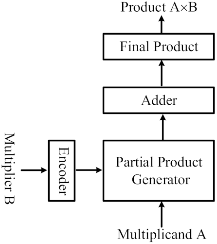
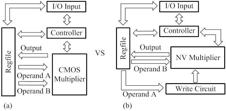
3. Proposed 8-bit Non-Volatile Booth Multiplier

In this paper, we present a scheme of an 8-bit non-volatile radix-4 booth multiplier. In our multiplier, we combine booth encoder with partial product generator, in which RRAM is used to configure and store multiplicand B. Therefore, the proposed multiplier has shorter latency and lower dynamic power. A novel readout circuit is also proposed to read out the partial product bits for subsequent addition. Considering the special output bits of partial product, we also simplify the full adder and 4-2 compressor in subsequent Wallace Tree. Finally, the Manchester carry chain is used as the final stage adder. The proposed RRAM-based multiplier structure diagram is shown in Figure 2, along with the cell of partial product generator array, analog-to-digital (AD) circuits, and two phase non-overlap clock circuit.
The structure of conventional CMOS-based computing system and non-volatile computing system is shown in Figure 3. In a conventional CMOS-based computing system, each computation requires to wait for the transfer of operands from the regfile to the CMOS-based multiplier. The regfile is designed to store the operands and outputs (see Figure 3a). The CMOS-based multiplier structure can be found in [44,45]. However, the non-volatile memory-based multiplier can avoid the migration of operand B when the frequency of change of B is not very high. The frequency of B can be reduced by proper algorithm and compilation of software. Because operand B is encoded in the RRAM array directly, which is already in the computing unit, there is no need for the operand B to migrate again (see Figure 3b). Thus, non-volatile memory-based multipliers have a low overall computation power and high speed. The non-volatile memory-based multiplier has been found in [3,46].
Our proposed multiplier has three main parts: the combination of booth encoding and partial product generator, adder tree (proposed Wallace tree), final adder (Manchester carry chain). These three parts are discussed in the following subsections.

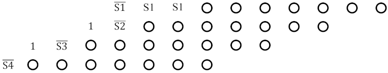
3.1. Booth Encoding and Partial Product Generator

Compared with the conventional booth multiplier structure in Figure 1, we try to combine the booth encoding unit with a partial product generator, shown in Figure 2.
As shown in Figure 2, we develop two multipliers dividing four partial products into two-row and one-row structures. The design of the two-row structure is similar to the one-row structure except for AD circuits. The two-row structure use only two kinds of ADs. However, the one-row structure uses four types of ADs. The detailed structural design of each cell of partial product array is shown in Figure 2.
As mentioned earlier, we use RRAMs to configure and achieve different booth encoding operations. For each cell shown in Figure 2, we use 4 RRAMs with 1T1R configuration to select different booth coding types: ± 2 A , ± 1 A or ± 0 A . Similarly, every cell should be set with the same pattern for the whole partial product array.
By setting different values to four types of RRAMs, we can implement booth encoding of multiplicand B. By taking B = 0110 0011 for example, we can simply get its booth encoding as + 2 A , 2 A , + 1 A , 1 A (most significant bit to least significant bit) [47], so the RRAM of each cell of partial product generator array is configured as below:
1.
‘−1A’ RRAM is LRS, others types are HRS;
2.
‘+1A’ RRAM is LRS, others types are HRS;
3.
‘−2A’ RRAM is LRS, others types are HRS;
4.
‘+2A’ RRAM is LRS, others types are HRS.
When the A i or A i 2 C = 1 , the transistor connected to corresponding branch switches on and we get a specific current. After converted by readout circuit, we get corresponding partial product bits.

3.2. Sign Bit

As for the 8-bit radix-4 booth multiplier, the partial product from booth encoding is extended to 15 bits by adding corresponding sign bits, which means more full adders are required.The conventional extension for partial products can be found in [47]. Actually, complexity can be reduced by using following method:
A two’s complement number can be written as:
S S S S S S S S Z 7 Z 6 Z 5 Z 4 Z 3 Z 2 Z 1
This pattern can be replaced by:
0 0 0 0 0 0 0 S Z 7 Z 6 Z 5 Z 4 Z 3 Z 2 Z 1
Since
s 2 14 + ( s 2 13 + s 2 12 + s 2 11 + s 2 10 + s 2 9 + s 2 8 ) = s 2 14 + s ( 2 14 2 8 ) = s 2 8
Then for 8-bit radix-4 booth multiplier, the four partial products can be simplified in [47]. For convenience of digital circuit design, we change the pattern as Figure 4.
With this method, we can significantly reduce the number of storage units for sign bits. In the above example that reflects booth encoding of ± 1 A , ± 1 A , ± 1 A , ± 1 A , we only need eight storage units for sign bits which is decreased by 60% compared to conventional extension [47]. Thus, using this method to reduce sign bits results in less area and power consumption.

3.3. Readout Circuit

One of the key components in our design is AD circuits. The ADs can be divided into four types: AD1b with one output bit, AD1.5b with two output bits, AD3b with three output bits and AD4b with four output bits. The schematic of AD1.5b shown in Figure 2d. The encoding of each type of AD is given in Table 2, with capacitance power. In terms of each branch of AD, only one RRAM can be set in each cell.
The AD1b is divided into two parts: (1) current sensing circuit changing load current into corresponding voltage V X ; (2) latched comparator to distinguish among states of different V X and latch the data.

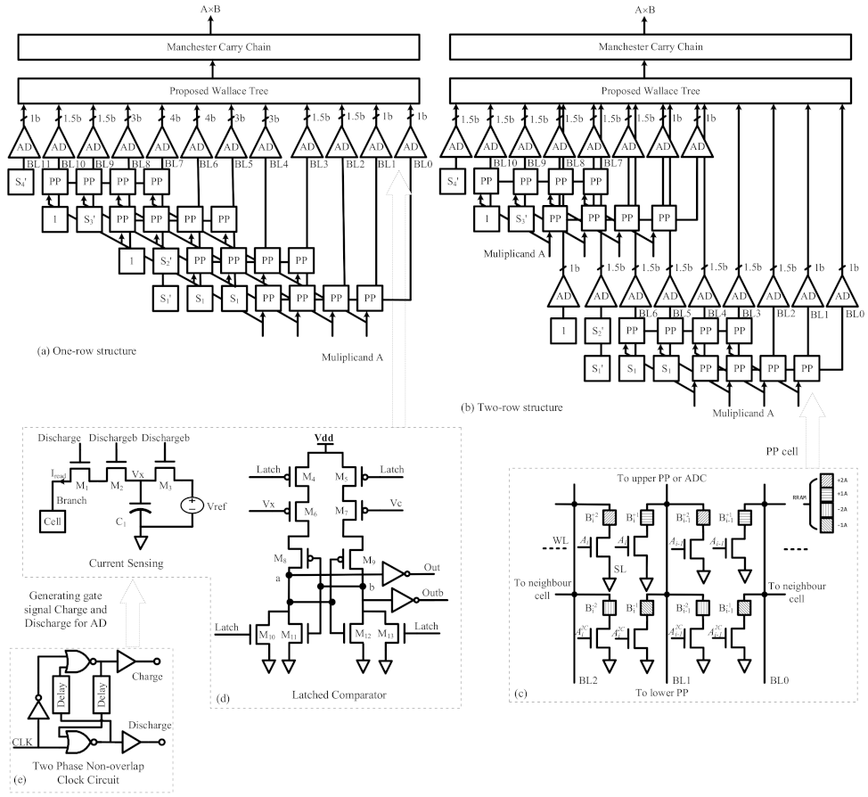
3.3.1. Current Sensing Circuit

The current sensing circuit is simply based on capacitance charge and discharge. The MOSFET M 1 controls discharge circuit while MOSFET M 3 controls charge circuit Figure 2d. The M 2 is used to reduce the effect of charge injection and clock feed-through effect when M 1 is closing.
In the charge circuit, when M 3 switches on and M 1 switches off, voltage reference charges the V X junction nearly to V r e f .
In the discharge circuit, when M 1 switches on and M 3 switches off, C 1 begins to discharge through load resistance which is connected to M 1 . As mentioned above, each branch will only have one of three different load resistance values: H R S 4 , L R S , and L R S 2 .The equation of discharge is given as:
V X = V r e f e t R C
With different resistance values, the rate of capacitance discharge is different. Thus, we can distinguish V X at the same time. To satisfy the design requirement, a two-phase non-overlap clock circuit is needed to generate gate signal Charge and Discharge shown in Figure 2e. Two delay units can regulate a non-overlap time on two sides. Using non-overlap clock has two major advantages: on the one hand, Charge and Discharge will not be valid concurrently at any time, in case that both charge circuit and discharge circuit switch on at the same time; on the other hand, when both these two signals are invalid, the capacitance-voltage V X can be latched for next comparison.
In order to get wide swing, a latched comparator is also needed so that the output swings between V D D and V S S .

3.3.2. Latched Comparator

The capacitance-voltage V X varies as mentioned above which causes the variation of current passing through M 6 . The current I M 6 is compared with the constant current generated by M 7 due to constant voltage V c . The M 10 , M 13 transistors are used to reduce kick-back noise, and the L a t c h signal voltage goes back to the input signal which may alter the data.
The value of V c should be set properly to distinguish between V O L , V O M I D and V O H or to distinguish between V O H , V O M I D and V O L . Resorting to this method, we can distinguish encoding between 0 and 1 for AD1b; Similarly, For AD1.5b, we need 2 latched comparators and 2 different values of V c to distinguish encoding among 00, 01 and 11.

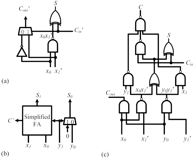
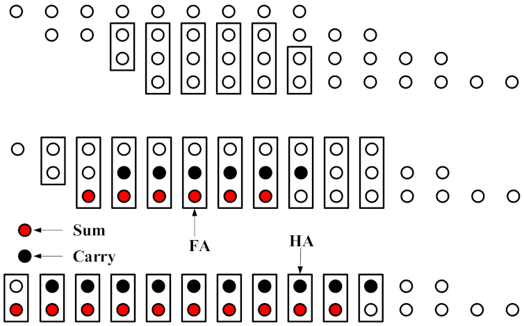
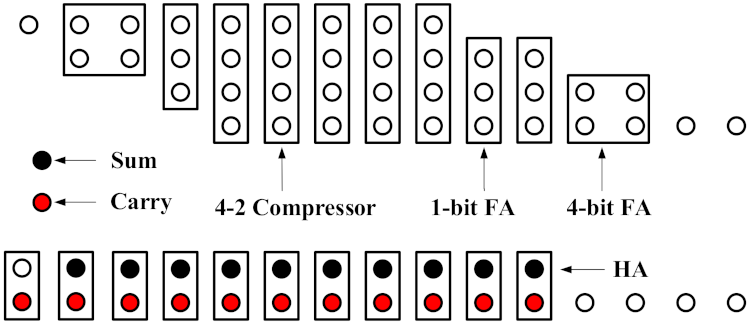
3.4. Proposed Wallace Tree

Conventional Wallace tree use carry-save adders to decrease critical path delay and the number of adder units [48]. However, in our design, the output signals O u t 0 and O u t 1 generated by the readout circuit only have 3 cases: 00, 10, 11. Thus, we can simplify the logic function of the 1-bit full adder, 4-bit adder, and 4-2 compressor so that we can further reduce the critical path delay and the number of transistors. For example, the truth table of simplified full adder is given in Table 3.
By depicting the corresponding K-map, we can get the simplified logic function of the proposed full adder. The schematic of full adder used in our work is shown in Figure 5a. Compared with a conventional full adder consisting of 28 transistors[49], our proposed full adder uses 26 transistors to achieve the same function. Furthermore, our full adder decreases the critical path delay, meaning the clock frequency has enough room to increase. Thus, the performance can be improved. Similarly, the 4-bit full adder and 4-2 compressor can also be simplified as shown in Figure 5b,c.
The conventional Wallace Tree diagram is shown in the Figure 6 and the proposed Wallace tree diagram, with above simplified key components, is demonstrated in Figure 7. Compared with the conventional Wallace tree [50], three stages are reduced to two stages in our work, which means fewer transistors and less area is used. Further, the speed of the whole multiplier is enhanced.

3.5. Manchester Carry Chain

At the final stage, we used an 11-bit Manchester carry chain to generate the final product. Compared with CLAs or other carry chains, the Manchester carry chain is simple and efficient. In the meantime, the worst case of the Manchester carry chain is when the carry chain discharges through the entire path, at which the path delay reaches the maximum. Besides, the Manchester carry chain is clock-controlled with pre-charge stage and discharge stage so that the output varies. Therefore, 15-bit D flip-flops are required to latch and synchronize the final result.The schematic of the Manchester carry chain can be found in [51].

3.6. Structure of Partial Product Generator

In Figure 2, we obtained the partial products in two ways: one-row and two-row. In the case of one-row, four partial products are needed, while in the case of two-row, only two partial products are needed in each row. Compared with the one-row structure in Figure 2a. The two-row structure in Figure 2a uses fewer types of AD circuits. However, some branches have more resistance values such H R S , L R S , L R S 2 , L R S 3 , L R S 4 , approximately. Therefore, the capacitance needs to discharge/charge for a little more time due to the presence of a smaller resistance value. New components AD3b and AD4b are also needed for some branches. One of the significant advantages of this one-row structure is the further improvement of our proposed Wallace tree. For example, in one-row structure, the output of AD4b only have five types: 0000, 0001, 0011, 0111 or 1111. So, a 4-2 compressor can be further simplified due to fewer input conditions. Similarly, the proposed 1-bit or 4-bit full adder can be also simplified.

4. Simulation Result and Comparison

The proposed non-volatile multiplier is implemented and simulated by a low v t 45 nm Generic Processing Design Kit (GPDK) with a supply voltage of 1 V and 1.2 V.

4.1. RRAM Circuit Simulation

The RRAM model is taken from [39] and modeled by Verilog-A. The key parameters of the RRAM model are shown in Table 4.
The MOSFET schematic diagram is shown in Figure 8b note that the gate of MOSFET is controlled by the word line (WL) with the source of the transistor connected to the source line (SL), while the drain is connected to the bit line (BL). The SET/RESET operation is performed by applying voltage pulses at the WL and BL/SL terminals. The DC switching IV characteristic of the RRAM to formulate radix-4 8 × 8 multiplier circuit is shown in Figure 8a. The device is simulated from −3 V to 3 V to obtain the IV-curve, which fits the results given in [39]. As shown in Figure 8a, the reading voltage is kept to 0.002 V in our design. The OFF/ON resistance is chosen as more than 100 to ensure the robustness of the RRAM design. while the reading voltage is less than the set voltage ( V t h = 1.5 V).
The simulation result of the OFF/ON resistance ratio is presented in Figure 8c. The resistance of LRS and HRS differs by two orders of magnitude, which meets the design requirements [35]. It is difficult to distinguish two states if the resistance has a difference of fewer than two orders of magnitude.

4.2. AD Circuit Simulation

The transient simulation of the current sensing circuit is performed, and the waveform of V X with two phase non-overlap clock is shown in Figure 9. When the Latch signal is valid (low), different data inputs A0 and A1 result in different V X .
In Figure 10, to verify the function of AD1.5bs, we change data input A 0 and A 1 to AD1.5b. In case, the L a t c h signal is valid (low), the correct conversion results O u t 0 and O u t 1 are valid.

4.3. Multiplier Circuit Simulation

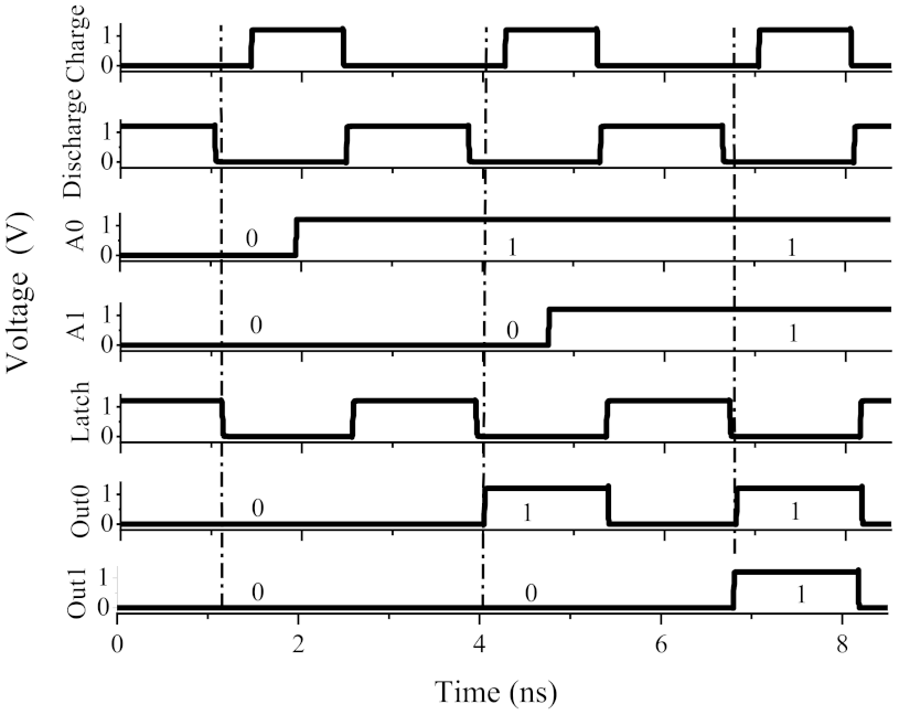
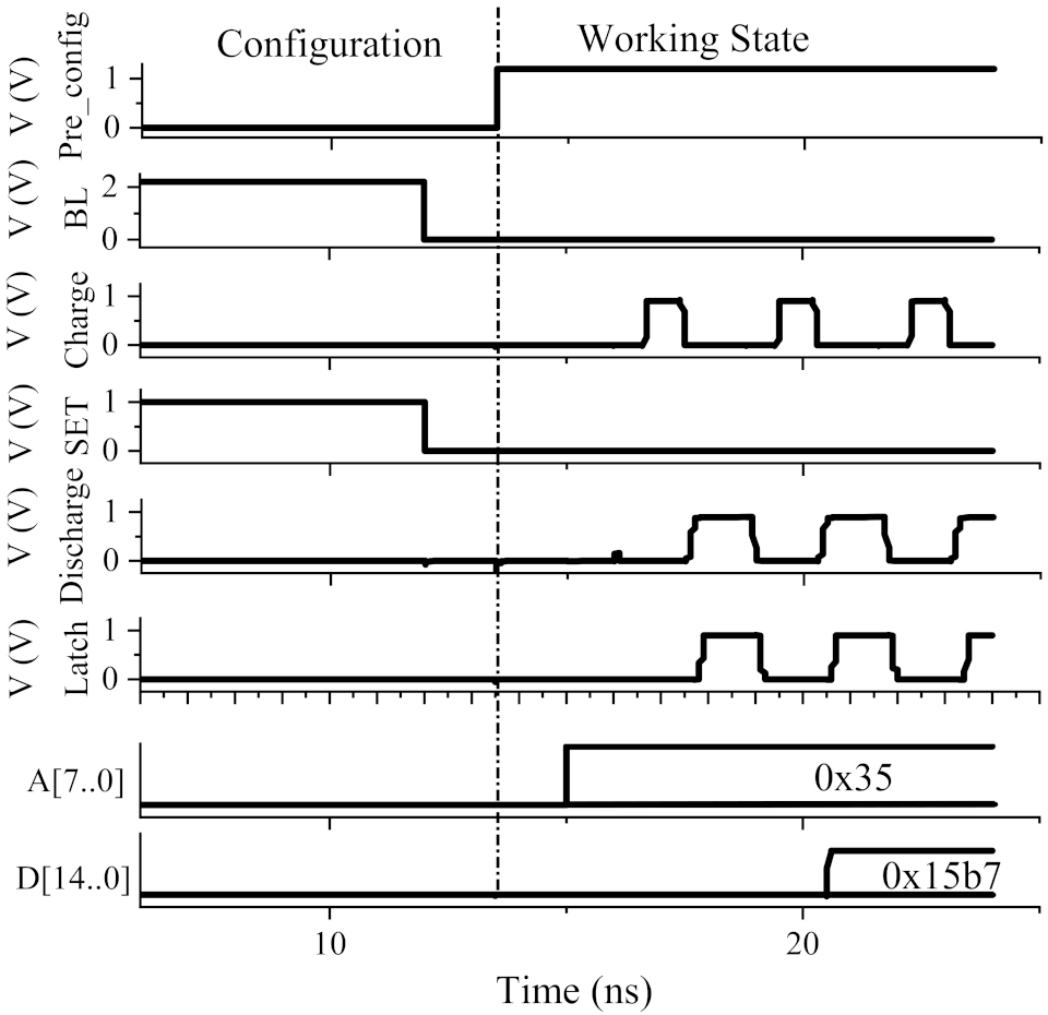
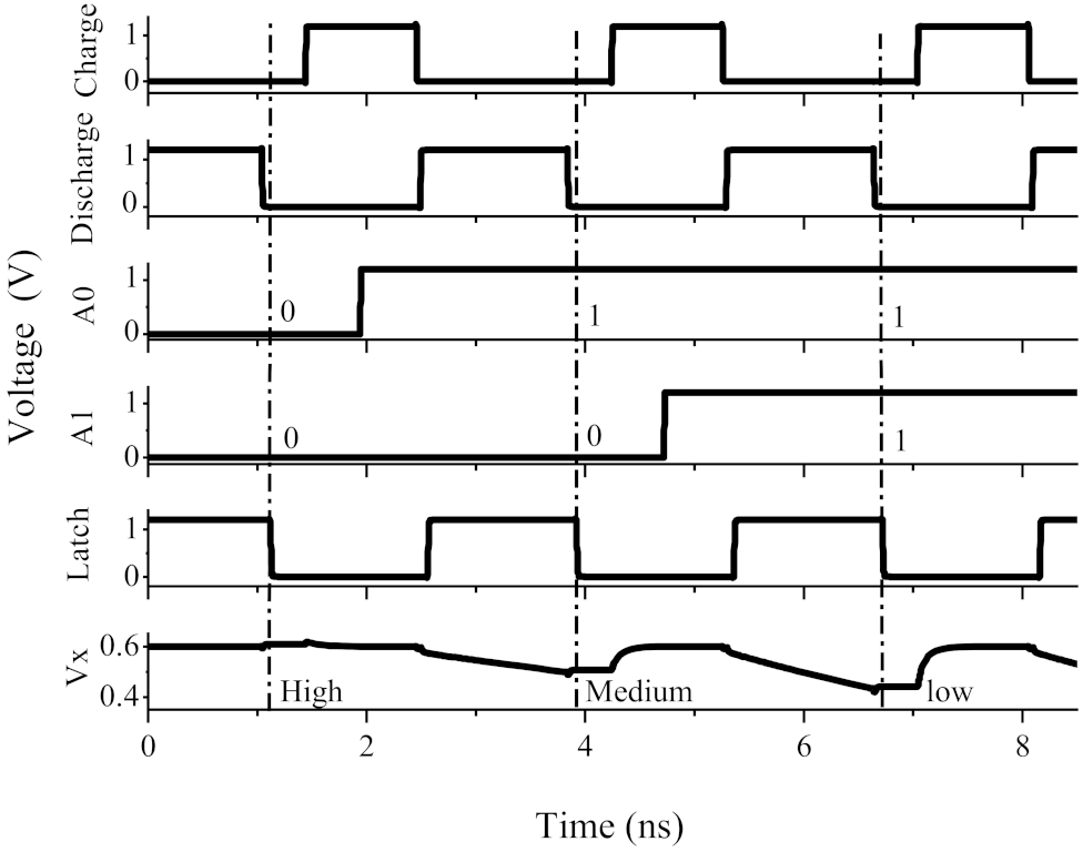
4.3.1. Transient Simulation Analysis
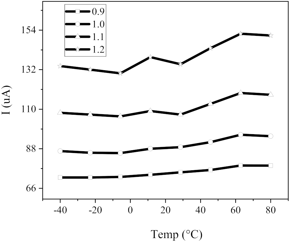
The transient simulation results of the proposed non-volatile booth multiplier are shown in Figure 11. In this simulation, multiplicand A = 01101101 is from external registers, while multiplicator B is configured as 00110011 for functional verification. D 0 , D 1 , D 2 , D 3 D 14 are final results. The configuration state and normal working state are separated and switched with transmission gates controlled by signal P r e _ c o n f i g . The branches of RRAM array are connected to setting pulse BL. S E T signal is used to configure 1T1R cells. D i s c h a r g e , C h a r g e and L a t c h are clock signals.
According to Figure 11, during configuration state, P r e _ c o n f i g signal is low. The corresponding RRAMs are set to LRS and multiplicator B is stored in RRAM when S E T becomes high. After 14 ns, P r e _ c o n f i g rises to high and the multiplier transits to normal working state. During this state, BL become high-impedance. The branches are connected to ADs, and the gate of transistors in 1T1R accept multiplicand A input.
In working state, we use primitive C L K signal to generate a two phase non-overlap clock C h a r g e and D i s c h a r g e . The initial voltage of the capacitance is set to 400 mV. Firstly, at the rising edge of D i s c h a r g e , discharge circuits are available and capacitances begin to discharge. When capacitance voltage falls to a certain value, D i s c h a r g e switches to be invalid (low) and the voltage becomes a constant V X . Then, at the falling edge of L a t c h , latched comparators compare the V x with given reference voltage V c and outputs partial products. At the rising edge of the C h a r g e , the outputs of latched comparators are latched and computed by proposed Wallace tree and the capacitances begin to recharge. When D i s c h a r g e is low, the Manchester carry chain is available. At this state, the outputs from wallace tree feed to Manchester carry chain for final addition. Finally, at the falling edge of C h a r g e , the DFFs output the multiplication result. Based on the input data, the output data should be 001010110110111. The simulation results show the proposed multiplier works correctly since that the waveforms of D 0 , D 1 , D 2 , D 3 D 14 meet with the expected data.

4.3.2. PVT Analysis

In this subsection, numerous simulations are conducted using the proposed architecture of multiplier to perform PVT analysis to authenticate the better working of the circuit under different processes, voltages and temperatures. The average input current and delay of the multiplier under SS, FF, MC (Monte Carlo) process is shown in Table 5, while keeping supply voltage at 1V and room temperature. As shown in Table 5, SS process has the lowest average current but largest delay. The highest average current is obtained under the FF process but with the smallest delay. The simulation of temperature and voltage sweep is carried out under MC process. The temperature is from −40 C to 80 C and supply voltage range is from 0.9 V to 1.2 V. If supply voltage is lower than 0.9 V, the multiplier can not work correctly. Figure 12 shows the temperature and voltage response curves of the average input current. The average input current increases and shows overall tendency to ascend with temperature.

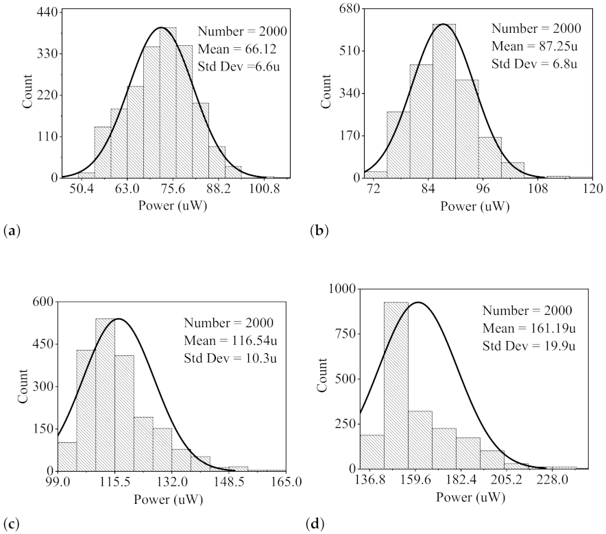
4.4. Performance Analysis and Comparison

In this subsection comparison of power, delay and area is presented. The factors are necessary to estimate and better understanding of the working efficiency of the resistive memory circuit design. Compared with conventional CMOS multipliers, our non-volatile multiplier has special characteristics in its partial product generator. Total power consumption in one computing cycle is the sum of the static and dynamic power of the CMOS circuit and energy consumed in capacitance charge/discharge of the circuit. The total power of the circuit is given as:
P s u m = P s t a t i c + P d y n a m i c + P c a p a c i t a n c e
Note, the capacitance charge and discharge once in each cycle. Therefore, the P c a p a c i t a n c e can be expressed more specifically as
P c a p a c i t a n c e = 1 2 C f V c h a r g e 2 + 1 2 C f V d i s c h a r g e 2
where, V c h a r g e and V d i s c h a r g e represent the difference between V X and V r e f while charging and discharging, respectively. Further, V X stable reading voltage and V r e f fully charged voltage.
Note in Equation (7), different V c h a r g e and V d i s c h a r g e result in different P c a p a c i t a n c e . Thus, to reduce the total power of the proposed multiplier circuits, the capacitance value should be kept low and the discharge time should not be much long. In the proposed multiplier, the CMOS parasitic capacitors are used as P c a p a c i t a n c e . Since the one-row structure and two-row structure have different numbers of current sensing circuits and different types of ADs, the values of P c a p a c i t a n c e obtained are different, as shown in Table 2. The supply voltage is kept at 1 V and V r e f = 0.4 V to get the result in Table 2. Note that P c a p a c i t a n c e of two structures are almost same. Dynamic power is the significant part of total power for the proposed multiplier. For different multiplicand A, the energy of one computing cycle is different. The transistors in the 1T1R structure are switched off when the multiplicand bits and two’s complement bits are 0. Thus, the partial product bits are 0 and the dynamic power is at minimum. Conversely, for all data bits are 1, the dynamic power is at maximum. Here, the worst case is used in comparison.
To verify the robustness of the proposed design to process and device mismatch, 2000 Monte Carlo simulation runs are performed at various voltages. Figure 13 shows the results of Monte Carlo analysis. The power consumption of the two-row multiplier is 66.12 μ W, 87.25 μ W, 116.54 μ W, and 161.19 μ W, corresponding to supply voltage 0.9 V, 1 V, 1.1 V, and 1.2 V, respectively. Further, the time delays of each part are t C L K = 257.8 ps, t A D = 404.4 ps, t w a l l a c e = 73.5 ps, t m a n c h e s t e r = 85.83 ps with supply voltage V d d = 1.2 V. The time delays of each part are t C L K = 307.7 ps, t A D = 528.4 ps, t w a l l a c e = 107.71 ps, t m a n c h e s t e r = 102.92 ps at supply voltage V d d = 1 V.
The multiplier circuits in [3,44,45] are simulated for the comparison. The critical parameters determining the effectiveness the multiplier are presented in Table 6. The proposed 8 bit radix-4 non-volatile parallel multiplier has better performance in terms of delay, power and PDP. For instance, the one-row and two-row multipliers have about 63% and 70% power and PDP reduction compared to the conventional radix-4 8 × 8 booth multiplier, respectively. The proposed multipliers have a 19% delay reduction on the same supply voltage condition. Since the proposed multipliers use 1T1R structure to integrate the booth encoder to the partial product generator, the area of the partial product generator is smaller. Additionally, the extra Manchester chain is employed to improve the power and delay of the proposed multipliers, which results in the extra area. Furthermore, the proposed multiplier is non-volatile, i.e., the data are not lost when the system is powered off. Thus, the reliability and security obtain further improvement.

4.5. System Power Comparison

The proposed RRAM-based non-volatile booth multiplier can be applied to neural networks, filters, and other similar applications. The RRAM-based systems include configuration mode, normal working mode. Configuration mode is used to configure system parameters. We mainly estimate the system power and compare it with the conventional computing system.
Power comparison: since total power consumption in one computing cycle is the sum of the static and dynamic power. There is no static power for the non-volatile computing system. However, there is static power for conventional computing systems. The conventional and non-volatile computing system both have the same power on loading A and computing but different in loading B. The conventional computing system needs to reload multiplicand B every time but non-volatile systems only need to load B once. This also helps to save power.
Data storing: In the conventional SRAM multiplier-based system [52], one SRAM cell consists of 6 transistors. By contrast, in the RRAM multiplier-based system, one storage unit only consists of one transistor and one RRAM. Also, the RRAMs can be 3D stacked to reduce storage area substantially.

5. Conclusions

In this paper, we have proposed an 8-bit RRAM-based non-volatile radix-4 booth multiplier. Specifically, partial product generator, Wallace tree, Manchester carry chain, and associated AD circuit structures are designed. A two-stage Wallace tree is designed for the proposed multiplier, which reduced time delay and area compared to the conventional Wallace tree. Furthermore, the use of non-volatile RRAM enables the multiplier to store multiplicand beforehand, reducing the overall computation time. The comparative results showed that the proposed multiplier has 70% less PDP, 63% lower power consumption, and 19% less delay than the regular CMOS-based radix-4 booth multiplier. The results suggest that our proposed multiplier could be a promising component in processing units. It can be employed in various low-power and high-speed applications, in which certain data will not frequently change, such as the weight of the convolutional neural network.

Author Contributions

Conceptualization, K.H. and X.Z.; methodology, K.H.; formal analysis, C.F.; investigation, C.F and X.Z.; data curation, C.F.; writing—original draft preparation, C.F.; writing—review and editing, X.Z. and K.H.; supervision, K.H.; project administration, X.Z.; funding acquisition, X.Z and Z.G.. All authors have read and agreed to the published version of the manuscript.

Funding

This research received funding of the Major Scientific Research Project of Zhejiang Lab(Grant No. 2019KC0AD02), Research Program of Department of Science and Technology of Zhejiang Province (LGF19H180019), and Research Program of Medical and Health Science and Technology Plan Project of Zhejiang Province under grant (2019PY033).

Conflicts of Interest

The authors declare no conflict of interest.

References

  1. Silver, D.; Huang, A.; Maddison, C.; Guez, A.; Sifre, L.; Driessche, G.; Schrittwieser, J.; Antonoglou, I.; Panneershelvam, V.; Lanctot, M.; et al. Mastering the game of Go with deep neural networks and tree search. Nature 2016, 529, 484–489. [Google Scholar] [CrossRef] [PubMed]
  2. LeCun, Y.; Bengio, Y.; Hinton, G. Deep Learning. Nature 2015, 521, 436–444. [Google Scholar] [CrossRef] [PubMed]
  3. Dai, L.; Guo, H.; Lin, Q.; Xia, Y.; Zhang, X.; Zhang, F.; Fan, D. An In-Memory-Computing Design of Multiplier Based on Multilevel-Cell of Resistance Switching Random Access Memory. Chin. J. Electron. 2018, 27, 1151–1157. [Google Scholar] [CrossRef]
  4. Von Neumann, J. First draft of a report on the EDVAC. IEEE Ann. Hist. Comput. 1993, 15, 27–75. [Google Scholar] [CrossRef]
  5. Reuben, J. Rediscovering Majority Logic in the Post-CMOS Era: A Perspective from In-Memory Computing. J. Low Power Electron. Appl. 2020, 10, 28. [Google Scholar] [CrossRef]
  6. Yuhao, W.; Xin, L.; Hao, Y.; Leibin, N.; Wei, Y.; Chuliang, W.; Junfeng, Z. Optimizing Boolean embedding matrix for compressive sensing in RRAM crossbar. In Proceedings of the 2015 IEEE/ACM International Symposium on Low Power Electronics and Design (ISLPED), Rome, Italy, 22–24 July 2015; pp. 13–18. [Google Scholar] [CrossRef]
  7. Cui, X.; Ma, Y.; Wei, F.; Cui, X. The Synthesis Method of Logic Circuits Based on the NMOS-Like RRAM Gates. IEEE Access 2021, 9, 54466–54477. [Google Scholar] [CrossRef]
  8. Zhang, S.; Huang, K.; Shen, H. A Robust 8-Bit Non-Volatile Computing-in-Memory Core for Low-Power Parallel MAC Operations. IEEE Trans. Circuits Syst. I Regul. Pap. 2020, 67, 1867–1880. [Google Scholar] [CrossRef]
  9. Zahoor, F.; Zulkifli, T.Z.A.; Khanday, F.A.; Zainol Murad, S.A. Carbon Nanotube and Resistive Random Access Memory Based Unbalanced Ternary Logic Gates and Basic Arithmetic Circuits. IEEE Access 2020, 8, 104701–104717. [Google Scholar] [CrossRef]
  10. Sahay, S.; Bavandpour, M.; Mahmoodi, M.R.; Strukov, D. Energy-Efficient Moderate Precision Time-Domain Mixed-Signal Vector-by-Matrix Multiplier Exploiting 1T-1R Arrays. IEEE J. Explor. Solid-State Comput. Devices Circuits 2020, 6, 18–26. [Google Scholar] [CrossRef]
  11. Ellaithy, D.M.; El-Moursy, M.A. A 90-nm CMOS Low-Energy Dual-Channel Serial/Parallel Multiplier. In Proceedings of the 2019 6th International Conference on Advanced Control Circuits and Systems (ACCS) 2019 5th International Conference on New Paradigms in Electronics Information Technology (PEIT), Hurgada, Egypt, 17–20 November 2019; pp. 132–135. [Google Scholar] [CrossRef]
  12. Huang, Z. High-Level Optimization Techniques for Low-Power Multiplier Design; University of California: Los Angeles, CA, USA, 2003. [Google Scholar]
  13. Oskuii, S. Design of Low-Power Reduction-Trees in Parallel Multipliers; Norwegian University of Science and Technology: Trondheim, Norway, 2008. [Google Scholar]
  14. Mishra, S. Design and Implementation of Faster and Low Power Multipliers; National Institute Of Technology: Rourkela, India, 2009. [Google Scholar]
  15. Jain, S.; Ranjan, A.; Roy, K.; Raghunathan, A. Computing in Memory With Spin-Transfer Torque Magnetic RAM. IEEE Trans. Very Large Scale Integr. (VLSI) Syst. 2018, 26, 470–483. [Google Scholar] [CrossRef]
  16. Kingra, S.K.; Vivek, P.; Che-Chia, C.; Hudec, B.; Tuo-Hung, H.; Manan, S. SLIM: Simultaneous Logic-in-Memory Computing Exploiting Bilayer Analog OxRAM Devices. Sci. Rep. 2020, 10, 2567. [Google Scholar] [CrossRef] [Green Version]
  17. Govoreanu, B.; Piazza, L.; Ma, J.; Conard, T.; Vanleenhove, A.; Belmonte, A.; Radisic, D.; Popovici, M.; Alin, V.; Redolfi, A.; et al. Advanced a-VMCO resistive switching memory through inner interface engineering with wide (>102) on/off window, tunable μA-range switching current and excellent variability. Dig. Tech. Pap.-Symp. VLSI Technol. 2016, 1–2. [Google Scholar] [CrossRef]
  18. Redolfi, A.; Goux, L.; Jossart, N.; Yamashita, F.; Nishimura, E.; Urayama, D.; Fujimoto, K.; Witters, T.; Lazzarino, F.; Jurczak, M. A novel CBRAM integration using subtractive dry-etching process of Cu enabling high-performance memory scaling down to 10 nm node. In Proceedings of the 2015 Symposium on VLSI Technology (VLSI Technology), Kyoto, Japan, 16–18 June 2015; p. 134. [Google Scholar] [CrossRef]
  19. Huang, K.; Zhao, R.; He, W.; Lian, Y. High-Density and High-Reliability Nonvolatile Field-Programmable Gate Array with Stacked 1D2R RRAM Array. IEEE Trans. Very Large Scale Integr. (VLSI) Syst. 2016, 24, 139–150. [Google Scholar] [CrossRef]
  20. Goux, L.; Fantini, A.; Kar, G.; Chen, Y.; Jossart, N.; Degraeve, R.; Clima, S.; Govoreanu, B.; Lorenzo, G.; Pourtois, G.; et al. Ultralow sub-500 nA operating current high-performance TiNAl2O3∖HfO2∖HfTiN bipolar RRAM achieved through understanding-based stack-engineering. In Proceedings of the 2012 Symposium on VLSI Technology (VLSIT), Honolulu, HI, USA, 12–14 June 2012; pp. 159–160. [Google Scholar] [CrossRef]
  21. ChiaHua, H.; Shen, T.Y.; Hsu, P.Y.; Chang, S.C.; Wen, S.Y.; Lin, M.H.; Wang, P.K.; Liao, S.C.; Chou, C.S.; Peng, K.M.; et al. Random soft error suppression by stoichiometric engineering: CMOS compatible and reliable 1Mb HfO2-ReRAM with 2 extra masks for embedded IoT systems. In Proceedings of the 2016 IEEE Symposium on VLSI Technology, Honolulu, HI, USA, 14–16 June 2016; pp. 1–2. [Google Scholar] [CrossRef]
  22. Waser, R.; Dittmann, R.; Staikov, G.; Szot, K. Redox-Based Resistive Switching Memories – Nanoionic Mechanisms, Prospects, and Challenges. Adv. Mater. 2009, 21, 2632–2663. [Google Scholar] [CrossRef]
  23. Wong, H.P.; Lee, H.; Yu, S.; Chen, Y.; Wu, Y.; Chen, P.; Lee, B.; Chen, F.T.; Tsai, M. Metal–Oxide RRAM. Proc. IEEE 2012, 100, 1951–1970. [Google Scholar] [CrossRef]
  24. Li, X.; Lai, L. Nonvolatile Memory and Computing Using Emerging Ferroelectric Transistors. In Proceedings of the 2018 IEEE Computer Society Annual Symposium on VLSI (ISVLSI), Hong Kong, China, 8–11 July 2018; pp. 750–755. [Google Scholar]
  25. Amirany, A.; Rajaei, R. Fully Nonvolatile and Low Power Full Adder Based on Spin Transfer Torque Magnetic Tunnel Junction with Spin-Hall Effect Assistance. IEEE Trans. Magn. 2018, 54, 1–7. [Google Scholar] [CrossRef]
  26. Huang, K.; Lian, Y. A Low-Power Low-VDD Nonvolatile Latch Using Spin Transfer Torque MRAM. IEEE Trans. Nanotechnol. 2013, 12, 1094–1103. [Google Scholar] [CrossRef]
  27. Meena, J.S.; Sze, S.M.; Chand, U.; Tseng, T.Y. Overview of emerging nonvolatile memory technologies. Nanoscale Res. Lett. 2014, 9, 526. [Google Scholar] [CrossRef] [PubMed] [Green Version]
  28. Ho, C.; Hsu, C.L.; Chen, C.C.; Liu, J.T.; Wu, C.S.; Huang, C.C.; Hu, C.; Yang, F.-L. 9 nm half-pitch functional resistive memory cell with 1 μA programming current using thermally oxidized sub-stoichiometric WOx film. In Proceedings of the 2010 International Electron Devices Meeting, San Francisco, CA, USA, 6–8 December 2010; pp. 19.1.1–19.1.4. [Google Scholar] [CrossRef]
  29. Govoreanu, B.; Kar, G.S.; Chen, Y.; Paraschiv, V.; Kubicek, S.; Fantini, A.; Radu, I.P.; Goux, L.; Clima, S.; Degraeve, R.; et al. 10 × 10 nm2 Hf/HfOx crossbar resistive RAM with excellent performance, reliability and low-energy operation. In Proceedings of the 2011 International Electron Devices Meeting, Washington, DC, USA, 5–7 December 2011; pp. 31.6.1–31.6.4. [Google Scholar] [CrossRef]
  30. Tsunoda, K.; Kinoshita, K.; Noshiro, H.; Yamazaki, Y.; Iizuka, T.; Ito, Y.; Takahashi, A.; Okano, A.; Sato, Y.; Fukano, T.; et al. Low Power and High Speed Switching of Ti-doped NiO ReRAM under the Unipolar Voltage Source of less than 3 V. In Proceedings of the 2007 IEEE International Electron Devices Meeting, Washington, DC, USA, 10–12 December 2007; pp. 767–770. [Google Scholar] [CrossRef]
  31. Banno, N.; Tada, M.; Sakamoto, T.; Miyamura, M.; Okamoto, K.; Iguchi, N.; Nohisa, T.; Hada, H. A fast and low-voltage Cu complementary-atom-switch 1 Mb array with high-temperature retention. In Proceedings of the 2014 Symposium on VLSI Technology (VLSI-Technology): Digest of Technical Papers, Honolulu, HI, USA, 9–12 June 2014; pp. 1–2. [Google Scholar] [CrossRef]
  32. Cheng, C.H.; Tsai, C.Y.; Chin, A.; Yeh, F.S. High performance ultra-low energy RRAM with good retention and endurance. In Proceedings of the 2010 International Electron Devices Meeting, San Francisco, CA, USA, 6–8 December 2010; pp. 19.4.1–19.4.4. [Google Scholar] [CrossRef]
  33. Kim, W.; Park, S.I.; Zhang, Z.; Yang-Liauw, Y.; Sekar, D.; Wong, H.P.; Wong, S.S. Forming-free nitrogen-doped AlOX RRAM with sub-uA programming current. In Proceedings of the 2011 Symposium on VLSI Technology—Digest of Technical Papers, Kyoto, Japan, 14–16 June 2011; pp. 22–23. [Google Scholar]
  34. Govoreanu, B.; Redolfi, A.; Zhang, L.; Adelmann, C.; Popovici, M.; Clima, S.; Hody, H.; Paraschiv, V.; Radu, I.P.; Franquet, A.; et al. Vacancy-modulated conductive oxide resistive RAM (VMCO-RRAM): An area-scalable switching current, self-compliant, highly nonlinear and wide on/off-window resistive switching cell. In Proceedings of the 2013 IEEE International Electron Devices Meeting, Washington, DC, USA, 9–11 December 2013; pp. 10.2.1–10.2.4. [Google Scholar] [CrossRef]
  35. Liu, S.; Wang, W.; Li, Q.; Zhao, X.; Li, N.; Xu, H.; Liu, Q.; Liu, M. Highly improved resistive switching performances of the self-doped Pt/HfO2:Cu/Cu devices by atomic layer deposition. Sci. China Phys. Mech. Astron. 2016, 59, 127311. [Google Scholar] [CrossRef]
  36. Jameson, J.R.; Blanchard, P.; Cheng, C.; Dinh, J.; Gallo, A.; Gopalakrishnan, V.; Gopalan, C.; Guichet, B.; Hsu, S.; Kamalanathan, D.; et al. Conductive-bridge memory (CBRAM) with excellent high-temperature retention. In Proceedings of the 2013 IEEE International Electron Devices Meeting, Washington, DC, USA, 9–11 December 2013; pp. 30.1.1–30.1.4. [Google Scholar] [CrossRef]
  37. Goux, L.; Belmonte, A.; Celano, U.; Woo, J.; Folkersma, S.; Chen, C.Y.; Redolfi, A.; Fantini, A.; Degraeve, R.; Clima, S.; et al. Retention, disturb and variability improvements enabled by local chemical-potential tuning and controlled Hour-Glass filament shape in a novel WWO3∖Al2O3∖Cu CBRAM. In Proceedings of the 2016 IEEE Symposium on VLSI Technology, Honolulu, HI, USA, 14–16 June 2016; pp. 1–2. [Google Scholar] [CrossRef]
  38. Wang, Z.; Su, Y.; Li, Y.; Zhou, Y.; Chu, T.; Chang, K.; Chang, T.; Tsai, T.; Sze, S.M.; Miao, X. Functionally Complete Boolean Logic in 1T1R Resistive Random Access Memory. IEEE Electron Device Lett. 2017, 38, 179–182. [Google Scholar] [CrossRef]
  39. Chen, P.; Yu, S. Compact Modeling of RRAM Devices and Its Applications in 1T1R and 1S1R Array Design. IEEE Trans. Electron Devices 2015, 62, 4022–4028. [Google Scholar] [CrossRef]
  40. Zheng, L.; Haimin, C.; Xianwen, Y. A hardware multiplier design of embedded microprocessor. In Proceedings of the 2010 IEEE International Conference on Information Theory and Information Security, Beijing, China, 17–19 December 2010; pp. 38–41. [Google Scholar] [CrossRef]
  41. Yeh, W.C.; Jen, C.W. High-speed Booth encoded parallel multiplier design. IEEE Trans. Comput. 2000, 49, 692–701. [Google Scholar] [CrossRef] [Green Version]
  42. Ping-hua, C.; Juan, Z. High-speed Parallel 32 × 32-b Multiplier Using a Radix-16 Booth Encoder. In Proceedings of the 2009 Third International Symposium on Intelligent Information Technology Application Workshops, Nanchang, China, 21–22 November 2009; pp. 406–409. [Google Scholar] [CrossRef]
  43. Xiaoping, C.; Wei, H.; Xin, C.; Shumin, W. A New Redundant Binary Partial Product Generator for Fast 2n-Bit Multiplier Design. In Proceedings of the 2014 IEEE 17th International Conference on Computational Science and Engineering, Chengdu, China, 19–21 December 2014; pp. 840–844. [Google Scholar] [CrossRef]
  44. Xue, H.; Patel, R.; Boppana, N.V.V.K.; Ren, S. Low-power-delay-product radix-4 8*8 Booth multiplier in CMOS. Electron. Lett. 2018, 54, 344–346. [Google Scholar]
  45. Kumar, G.G.; Sahoo, S.K. Implementation of a high speed multiplier for high-performance and low power applications. In Proceedings of the 2015 19th International Symposium on VLSI Design and Test, Ahmedabad, India, 26–29 June 2015; pp. 1–4. [Google Scholar] [CrossRef]
  46. Lee, J.; Eshraghian, J.K.; Cho, K.; Eshraghian, K. Adaptive Precision CNN Accelerator Using Radix-X Parallel Connected Memristor Crossbars. arXiv 2019, arXiv:1906.09395. [Google Scholar]
  47. Kuang, S.; Wang, J.; Guo, C. Modified Booth Multipliers With a Regular Partial Product Array. IEEE Trans. Circuits Syst. II Express Briefs 2009, 56, 404–408. [Google Scholar] [CrossRef]
  48. Balaji, V.S.; Upadhyay, H.N. FPGA implemenation of high speed and low power carry save adder. IIOAB J. 2016, 7, 151–159. [Google Scholar]
  49. Ghosh, A.; Ghosh, D. Optimization of Static Power, Leakage Power and Delay of Full Adder Circuit Using Dual Threshold MOSFET Based Design and T-Spice Simulation. In Proceedings of the 2009 International Conference on Advances in Recent Technologies in Communication and Computing, Kottayam, India, 27–28 October 2009; pp. 903–905. [Google Scholar] [CrossRef]
  50. Aradhya, H.V.R.; Madan, H.R.; Suraj, M.S.; Mahadikar, M.T.; Muniraj, R.; Moiz, M. Design and performance comparison of adiabatic 8-bit multipliers. In Proceedings of the 2016 IEEE Distributed Computing, VLSI, Electrical Circuits and Robotics (DISCOVER), Mangalore, India, 13–14 August 2016; pp. 141–147. [Google Scholar]
  51. Subash, T.; Ajaiyan; Subha, T. Performance Comparison of 64-bit Carry Look-Ahead Adders Using 32 nm CMOS Technology. Mater. Today Proc. 2017, 4, 4153–4168. [Google Scholar] [CrossRef]
  52. Takayanagi, T.; Nogami, K.; Hatori, F.; Hatanaka, N.; Takahashi, M.; Ichida, M.; Kitabayashi, S.; Higashi, T.; Klein, M.; Thomson, J.; et al. 350 MHz time-multiplexed 8-port SRAM and word size variable multiplier for multimedia DSP. In Proceedings of the 1996 IEEE International Solid-State Circuits Conference, Digest of TEchnical Papers, ISSCC, San Francisco, CA, USA, 10 February 1996; pp. 150–151. [Google Scholar] [CrossRef]
Figure 1. Conventional booth multiplier structure.
Electronics 10 02358 g001
Figure 2. One-row and two-row multiplier circuits with relevant critical components. The proposed 8-bit radix-4 non-volatile parallel multiplier has two kinds of structures: one-row structure and two-row structure. Both two kinds of structures consist of partial product (PP) generator array, AD, simplified Wallace tree, and Manchester carry chain. (a) Two-row structure of the proposed multiplier with 2 kinds of AD. (b) One-row structure of the proposed multiplier with 4 kinds of AD. (c) The key components of the Wallace tree including adders and compressors. (d) The cell of partial product generator array. (e) The read-out circuit (AD1.5b). AD contains the current sensing circuit and latched comparator. A two-phase non-overlap clock circuit is needed to generate gate signal Charge and Discharge.
Electronics 10 02358 g002
Figure 3. Computing system structure using different multipliers. (a) CMOS-based Multiplier [44,45]. (b) NVM-Based Multiplier [3,46].
Electronics 10 02358 g003
Figure 4. Generation of modified partial products for Radix-4 booth multiplier.
Electronics 10 02358 g004
Figure 5. (a) Proposed full adder (FA). (b) 4-bit full adder. (c) Simplified 4-2 compressor.
Electronics 10 02358 g005
Figure 6. Conventional Wallace tree with three stages.
Electronics 10 02358 g006
Figure 7. Proposed Wallace tree with two stages.
Electronics 10 02358 g007
Figure 8. (a) The IV curves [35]. (b) Schematic of a single 1T1R structure. (c) The resistance distribution diagram of RRAM [35].
Electronics 10 02358 g008aElectronics 10 02358 g008b
Figure 9. Transient simulation of current sensing circuit considering different combinations of data inputs A 0 and A 1 .
Electronics 10 02358 g009
Figure 10. Transient simulation of AD1.5b considering different combinations of data inputs A 0 and A 1 .
Electronics 10 02358 g010
Figure 11. Transient simulation of an 8-bit radix-4 non-volatile parallel multiplier with multiplicator B = 00110011 .
Electronics 10 02358 g011
Figure 12. Simulation of proposed proposed two-row multiplier to temperature and voltage sweep.
Electronics 10 02358 g012
Figure 13. The results of Monte Carlo analysis for total power of proposed two-row multiplier. (a) V d d = 0.9 V. (b) V d d = 1.0 V. (c) V d d = 1.1 V. (d) V d d = 1.2 V.
Electronics 10 02358 g013
Table 1. Multiplier Circuit Comparison [11,14].
Shift & AddArray MultiplierModified Booth MultiplierModified Booth Wallace Multiplier
Serial/ParallelSerialParallelParallelParallel
AreaSmallLargeMediumMedium
Power ConsumptionSmallLargeMediumMedium
DelayLargeMediumSmallSmallest
ComplexitySimpleSimpleComplexComplex
ImplementationEasyEasyMediumDifficult
Table 2. Number of ADs and total P c a p a c i t a n c e in two structures.
Type V x min (mV)One-RowTwo-RowCoding
AD1b253360,1
AD1.5b18341700,10,11
AD3b13230000,001,011,111
AD4b100500000,0001,0011,0111,1111
P c a p a c i t a n c e ( μ W)4.924.99-
Table 3. Truth table of simplified full adder.
ResistanceX0X1CinSCout
R H 4 00000
R H 4 00110
/010XX
/011XX
R H 3 / / R L 10010
R H 3 / / R L 10101
R H 2 / / R L 2 11001
R H 2 / / R L 2 11111
Table 4. Key parameters of the RRAM model.
ParameterDescriptionDefault Value
LOxide thickness5 nm
gap_minMin. gap distance0.1 nm
gap_maxMax. gap distance1.7 nm
gap_iniInitial gap distance1.367 nm
a0Atomic distance0.25 nm
EagActivation energy for vacancy generation1.501 eV
EarActivation energy for vacancy recombination1.5 eV
I0I-V fitting parameter 3 × 10 5
g0I-V fitting parameter 1.8819 × 10 10
V0I-V fitting parameter4.3
v 0 Gap dynamics fitting parameter150
γ 0 Gap dynamics fitting parameter16.5
g 1 Gap dynamics fitting parameter 1 × 10 9
β Gap dynamics fitting parameter1.25
Table 5. Average current of the two-row multiplier under different process.
ProcessMCFFSS
Average Current ( μ A)89.8134.075.4
Delay (ns)1.050.901.38
Table 6. Comparison of conventional booth multipliers [44,45]. NVM-based multipliers [3,46] and the proposed multiplier.
Process (nm) V dd (V)Delay (ns)Power ( μ W)PDP (fJ)Area ( μ m 2 )MemoryPDP Save (%)
[44]901.21.04435.9453regular CMOS0
[3]651.21.03335345.05738.23RRAM23
[45]651.321.04358372749.12regular CMOS17
[46]1801.21200RRAM
Proposedtwo-row451.20.83161.19133.80785.20RRAM70
one-row451.20.83135.72112.65749.61RRAM75
two-row4511.0587.2591.52785.20RRAM79
two-row4511.0579.1983.15749.61RRAM81
Publisher’s Note: MDPI stays neutral with regard to jurisdictional claims in published maps and institutional affiliations.

