Abstract
This paper reveals the relationship between the Miller plateau voltage and the displacement currents through the gate–drain capacitance () and the drain–source capacitance () in the switching process of a power transistor. The corrected turn-on Miller plateau voltage and turn-off Miller plateau voltage are different even with a constant current load. Using the proposed new Miller plateau, the turn-on and turn-off sequences can be more accurately analyzed, and the switching power loss can be more accurately predicted accordingly. Switching loss models based on the new Miller plateau have also been proposed. The experimental test result of the power MOSFET (NCE2030K) verified the relationship between the Miller plateau voltage and the displacement currents through and . A carefully designed verification test bench featuring a power MOSFET written in Verilog-A proved the prediction accuracy of the switching waveform and switching loss with the new proposed Miller plateau. The average relative error of the loss model using the new plateau is reduced to 1/2∼1/4 of the average relative error of the loss model using the old plateau; the proposed loss model using the new plateau, which also takes the gate current’s variation into account, further reduces the error to around 5%.
1. Introduction
Integrated power management and conversion circuitry is a fundamental block in many emerging applications such as Internet of Things (IoT) systems [1,2] and wearable healthcare devices, which are usually powered by batteries and energy harvesters [3,4]. The power consumption of these devices needs to be minimized to prolong the battery lifetime and improve the usability in inaccessible environments, requiring highly efficient DC-DC converters. In recent years, the operating frequency of the converter has been continuously increasing [5,6,7,8] to achieve higher power efficiency, faster speed, and higher power density. In addition to the consideration of topologies and control strategies [9,10,11,12], the switching process and the switching loss of the power switches are playing more important roles in a high-frequency DC-DC converter. The transient behavior of a power transistor can cause power dissipation and overvoltage, overcurrent, or even ringing [13,14,15,16,17], which are related to the system efficiency, maximum voltage or current ratings of the power transistor, and the electromagnetic interference (EMI) property of the system. Therefore, in-depth analysis of the switching process and more accurate switching loss models are necessary to ensure better performance and maintain the high efficiency of the switching mode power supply (SMPS) working at a higher and higher switching frequency.
Obviously, the switching behavior can be reproduced accurately with simulators such as Spectre and HSpice, but the simulation-based approach fails to provide intuitive understanding [18,19], which is helpful in circuit design. On the other hand, an analytical model with reasonable simplifications provides closed-form mathematical equations, which show the relationship between the device loss and key parameters. These equations can be further used to optimize the power transistors. The conventional piecewise-linear model [20,21,22] is simple and effective in a capacitance-limited case, but not suitable for the latest generation of low-voltage power MOSFETs where the parasitic inductance limits the switching process. Many new analytical models [18,23,24,25,26,27,28] with different tradeoffs between accuracy and complexity have been proposed to analyze the switching process and switching loss. These analytical models are more application-specific and may even include the nonlinearity of the capacitors of the devices. Reference [27] aimed at superjunction MOSFETs and demanded the unusual extraction of electrical characteristics from regular datasheets. Reference [28] only analyzed output capacitance-related losses in wide-bandgap transistors and did not include other kinds of switching losses. Effective figures of merit (FOMs) [29,30] of the power transistors have also been proposed to measure the device performance and help to select the right design parameters of power transistors. Nevertheless, providing an analytical model of the power transistor’s switching process and switching power loss with high accuracy is still very challenging. With the least added complexity, loss models developed directly from the classical piecewise-linear model that can still provide accurate prediction are especially attractive.
One major reason for the limited accuracy of the analytical switching loss models is that the so-called Miller plateau is difficult to predict. The Miller effect has long been a well-known phenomenon, and the Miller plateau observed in the switching process of a power transistor is related to this effect. In the conventional or the newly proposed analytical models [20,24,27,30], the Miller plateau voltage has proven to be useful in analyzing the switching process and calculating switching loss. In existing analytical models, the value of is defined as the gate–source voltage when the channel current equals the load current. However, as revealed in this paper, the Miller plateau voltage also relates to the gate driving voltage and the displacement currents through and . A more precise Miller plateau voltage will improve the accuracy of the calculated switching loss.
In this paper, we analyze the Miller effect in the switching operation of power MOSFETs thoroughly and provide a more accurate Miller plateau including the displacement currents through the parasitic capacitances. As a result, the switching process and the switching loss can be analyzed more accurately: the average relative error of the loss model using the new Miller plateau is reduced to 1/2∼1/4 of the one obtained by the traditional Miller plateau. The rest of the paper is structured as follows: the new model for accurate Miller plateau estimation is proposed in Section 2. Based on the corrected Miller plateau voltage, the switching process and the switching power loss are analyzed in Section 3. Experimental and simulation results are provided in Section 4, verifying the proposed analysis method using the new Miller plateau. Finally, the conclusion is given in Section 5.
2. Miller Plateau Corrected with Displacement Currents
Figure 1a shows a traditional boost converter, which is a widely used step-up DC-DC converter. Since the duration of the turn-on time or turn-off time is much smaller than the switching period , the inductance L may be considered to be a constant current source and the output capacitance C a constant voltage source during the switching transitions. With these assumptions and a simple rearrangement of the circuit elements, the equivalent circuit shown in Figure 1b is obtained, which is used to analyze the switching process in this paper. It has been proven that this equivalent circuit can also be utilized to analyze the switching process of other SMPS topologies [18,31,32].
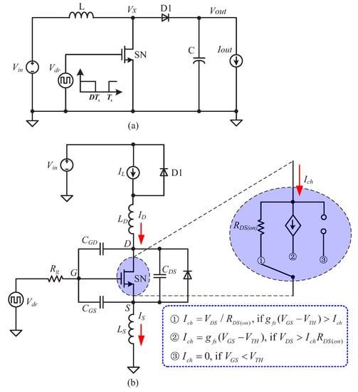
Figure 1.
(a) Boost converter with practical realization using a MOSFET and diode; (b) MOSFET switch with a partially clamped current load (three states of the MOSFET: 1 → ON, 2 → ACTIVE, 3 → OFF).
As was clarified in [32] that the basic transistor action is fast enough, which makes solving the physical equations governing the device behavior simultaneously with the circuit equations unnecessary, and we can safely rely on the fact that what decides the switching process is the time required to establish voltage changes across the parasitic capacitances and current changes in the parasitic inductances. The parasitic capacitances mainly comprise the three interelectrode capacitances, namely , , and . The parasitic inductances of the drain and source leads, and , must also be considered in high-frequency SMPS. These parasitic capacitances and inductances are also indicated in Figure 1b. Although the capacitances of the devices manifest great nonlinearity, methods as shown in [24] can be adopted to estimate the effective value of each capacitance. To simplify the discussion, we here use the effective values of , , and and omit their nonlinearity.
In Figure 1b, the transistor SN used as a power switch is a MOSFET. In a monolithic low-voltage DC-DC converter, those integrated power switches are no more than standard CMOS MOSFETs, only that there are thousands of elementary cells in parallel with each other and usually bearing at least 1 A current in the ON state [33]. Figure 1b also gives the equivalent circuit of the MOSFET and its three states.
Both the source inductor and the gate–drain capacitor form negative feedbacks from the drain circuit to the gate circuit. The former slows down the gate circuit, creating more switching loss, while the latter causes the Miller effect [34,35,36]. The Miller effect shows that the equivalent input capacitance related to is multiplied by , where A denotes the voltage gain from to . The observed Miller plateau in the switching process of a power transistor is a result of the Miller effect. When the load current of the power transistor is , the Miller plateau of is traditionally [20,21,22,24] defined as:
where is the MOSFET’s transconductance and is its typical threshold voltage.
According to (1), the turn-on Miller plateau voltage and turn-off Miller plateau voltage are the same with a constant current load, and few papers have mentioned the impact of the displacement currents through and on the Miller plateau. Reference [27] defined a current that correlates with the displacement current, but its value was calculated empirically by observing patterns in the simulated waveforms, and only the displacement current through was considered.
During the switching process, the current flowing through the transistor is not equal to the load current, namely . As shown in Figure 1b, the displacement currents flowing through and must also be included. According to Kirchhoff’s current law (KCL) for node D in Figure 1b, it is derived that:
With an ideal current source load, the voltage gain , and this equals an infinite capacitance according to the Miller effect. When reaches the Miller plateau during the turn-on process, all the gate current flows into , but there is no voltage increase of . As a result, the voltages of the gate node G and the source node S are both constant, and their rate of change is zero. Therefore, , and . Then,
The current flowing into is now , and the current flowing out of and in parallel is now . Substituting and the capacitor’s current–voltage relationship into (3), it is deduced that:
This equation reveals the relationship between the turn-on Miller plateau and the two displacement currents through and .
Similarly, when reaches the Miller plateau during the turn-off process, the current flowing out of is and the current flowing into and in parallel is . Substituting and the capacitor’s current–voltage relationship into (3), it is deduced that:
This equation reveals the relationship between the turn-off Miller plateau and the two displacement currents through and .
From (4) and (5), the Miller plateau voltages of the turn-on process and turn-off process are derived as:
This equation shows that the two Miller plateau voltages of the turn-on and turn-off processes are different even with a constant current load. This can be better explained by realizing that a Miller plateau voltage of also means a Miller plateau current of . Since the MOSFET is in the ACTIVE state during the Miller time, the turn-on Miller plateau current and turn-off Miller plateau current are:
With the capacitances being considered, the channel current must be larger than the load current during the turn-on process and smaller than the load current during the turn-off process to provide the extra displacement currents through and . The traditional value of in (1) does not take the displacement currents into account and assumes that when reaches the Miller plateau during the switching process; thus, the Miller plateau is the same in both the turn-on and turn-off process. As will be shown in the following sections, using the new assessment of the Miller plateau voltage, the switching process and switching power loss can be more accurately analyzed, especially for the low-voltage, high-frequency SMPS.
3. Analyzing the Switching Process and Switching Loss with the New Miller Plateau
The new Miller plateau voltage shown in (6) can be easily applied to the conventional piecewise-linear model or other analytical models. In the turn-on process, the traditional Miller plateau voltage should be replaced by ; in the turn-off process, should be replaced by .
3.1. Switching Waveform Analysis Using the New Miller Plateau
The turn-on or turn-off transition of a power transistor follows several distinct intervals [18,20,32]. Figure 2 illustrates the switching waveforms of a power MOSFET with a clamped current load. Both the turn-on and the turn-off switching processes are divided into five intervals. In Figure 2, each interval of the turn-on sequence is marked by , and each interval of the turn-off sequence is marked by . On the top of the figure, the corresponding state of the MOSFET in each interval is also indicated with the same mark (three states of the MOSFET: 1 → ON, 2 → ACTIVE, 3 → OFF) in Figure 1b.
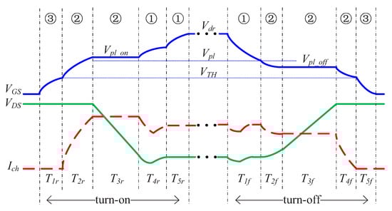
Figure 2.
The turn-on sequence and turn-off sequence of a power MOSFET with a clamped current load.
In the turn-on sequence, the first interval is the delay time , during which ramps up to . Next comes the current increase phase, during which continues ramping up to the Miller voltage . The channel current also reaches its Miller plateau, a value larger than the load current . is the Miller time, and falls from to zero with a constant rate . Entering , the MOSFET has already gone into the ON state. This is the time needs to change from its Miller value to its final state. The time constant in this interval is . The final interval sees complete its rise toward .
In the turn-off sequence, the first interval is the delay time , during which ramps down to . Next comes the interval during which continues ramping down to the Miller voltage . The channel current also reaches its Miller plateau, a value smaller than the load current . is the Miller time, and rises from zero to with a constant rate . Entering , the MOSFET is still in the ACTIVE state. This is the time needs to change from its Miller value to zero. The final interval sees complete its fall toward zero.
According to the above analysis, the equivalent circuit of each interval is first-order, whose solution can be easily obtained. For example, during the delay time , the gate–source voltage rises exponentially towards with a time constant given by (), that is,
The delay time lasts until . Thus, is derived as follows:
Table 1 gives the duration of each interval of the switching process. As and indicate, when is larger than , the turn-on sequence is believed to be over; when is smaller than , the turn-off sequence is believed to be over.

Table 1.
Duration of each interval of the switching process of a power MOSFET with a clamped current load.
Figure 2 and Table 1 analyze the switching process of the capacitance-limited (the parasitic and are small enough to be neglected) case with a clamped current load. However, the proposed new Miller plateau can be used to analyze the switching process under other conditions only if some revisions are made.
For example, with a resistive load , remains unchanged. However, the duration of the following intervals must be changed since the load current now varies during the switching process. can be calculated with the same equation in Table 1 with a new value of @ . The value of @ , together with , can be used to calculate :
If cannot be ignored, the time constant of is instead of since acts as a current source during this interval. Reference [32] showed that, in the turn-on sequence, depending on which, the gate circuit and drain circuit, is faster, the drain voltage will collapse before there is any appreciable rise in current, or the current will reach its Miller value before the drain voltage collapses. This actually equals whether there is a Miller plateau in the turn-on sequence or not. If is small, there will be a Miller plateau in the turn-on sequence and the channel current will finish its rise earlier. From the analysis of [32], varies according to a quadratic function during the main transition interval. Then, the rate of the rise will accelerate, and this means an abrupt change when it enters its Miller plateau. With the new value of , we can make it rise smoothly since still needs to change from to during in Figure 2.
There will always be a Miller plateau in the turn-off process even in the inductance-limited case (the drain voltage collapses before the channel current finishes its rise in the turn-on process). However, during , must rise above to discharge . Using the same method as in [32] with the new Miller plateau of the turn-off process to analyze the switching action during ,
where and . Thus:
In all, using the new Miller plateau voltages and , the switching waveforms can be analyzed under various load conditions. Parasitic inductances can also be included. No detail is missed; each interval has its own physical meaning, and the duration thereof can be easily calculated, which greatly helps to comprehend the switching process of the power MOSFET.
3.2. Switching Loss Analysis Using the New Miller Plateau
The above analysis shows that it is rather easy to use the new Miller plateau voltages and to analyze the switching process of a power transistor. With the switching waveforms being known, it is straightforward to calculate the corresponding turn-on and turn-off losses by calculating the integral of over the switching time. Since the analyzed switching waveforms are accurate, the calculated switching losses will be accurate as well.
To simplify the discussion and make a better comparison, we here directly cite the closed-form loss model of [30]:
where ; and represent turn-on switching loss and turn-off switching loss, respectively, and is the switching frequency. This equation differs a little from its original expression in [30]. In [30], the gate charge was used instead of the capacitance. Although the capacitances of a power transistor manifest great nonlinearity, methods as shown in [24] can be adopted to estimate the effective value of each capacitance. After the new Miller plateau is calculated with the capacitance’s effective value, the gate charge can still be used. To simplify the discussion, we here use the effective values of , , and and omit their nonlinearity.
Based on (13), the new and in (6) are used instead of the conventional , and the corresponding and in (7) are also used to replace the load current . Then,
In (13) and (14), the gate current was assumed to be constant during the switching process, namely in the turn-on process and in the turn-off process. However, this makes sense only during the Miller time of the switching process. When changes from to in the turn-on process or from to in the turn-off process, the gate current varies greatly. It is necessary to make a more accurate assessment of the gate current during this time to further improve the prediction accuracy of the switching power loss, especially for the low-voltage, high-frequency SMPS.
Using the average gate current when changes from to in the turn-on process or from to in the turn-off process, (14) can be further written as:
in which and are the average gate current when changes from to in the turn-on process and the average gate current when changes from to in the turn-off process, respectively. Their values are approximated as:
which is a simple linear approximation.
Simply replacing the traditional Miller plateau with the proposed new Miller plateau will improve the prediction accuracy of the existing loss models. In addition, unlike previous works, we here directly analyzed instead of . In this way, it is clear that the widely accepted output capacitance loss term is redundant [25]. If the capacitance’s effect on the switching duration has already been included, there is no need to further add the output capacitance loss to the final calculation of the switching loss.
4. Experimental and Simulation Verification
4.1. Experimental Test Result of the Miller Plateau
Shown in Figure 3, the experimental validation of the newly calculated Miller plateau was carried out by testing NCE2030K [37] with an equivalent load current A. The input voltage was 10 V, and the gate driving voltage was 3 V. The nominal values of NCE2030K’s key parameters were: , , (@ ), (@ ), pF (@ ).
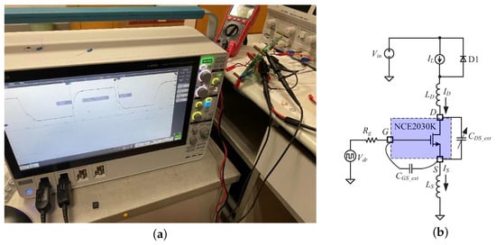
Figure 3.
(a) Experimental validation of the newly calculated Miller plateau by testing NCE2030K; (b) testing setup of NCE2030K.
The circuit was driven directly by the signal generator whose 50 output impedance served as . The driving signal was 100 kHz with a 50% duty cycle. An external 2 nF capacitance was also connected in parallel with the power MOSFET.
The relatively low-frequency operation and the added capacitors made the gate circuit slow and reduced the effect of parasitic inductances, which ensured that the Miller plateau voltages could be accurately measured.
The measured switching waveforms of and are shown in Figure 4, where the Miller plateau of can be readily identified from its waveform. As shown in this figure, the turn-on Miller plateau voltage and the turn-off Miller plateau voltage are different, which cannot be explained by the existing calculation method of the Miller plateau in (1). In contrast, the proposed calculation method of the Miller plateau in (6) shows that the two Miller plateau voltages of the turn-on and turn-off processes are different even with a constant current load. (6) also reveals that the Miller plateau correlates with the relevant capacitances.
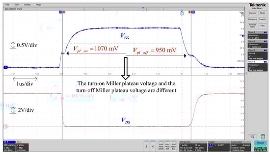
Figure 4.
Measured switching waveforms of and for NCE2030K when V, A, and .
Table 2 shows the measured (Meas.) Miller plateau, the predicted Miller plateau by the existing (Exist.) method, and the predicted Miller plateau by the proposed (Prop.) method when the relevant capacitance changes. Substituting the above circuit parameters into (1), the predicted Miller plateau by the existing method is 710 mV in both the turn-on and turn-off switching processes and has no relationship with the relevant capacitances. Substituting the above circuit parameters into (6), the predicted Miller plateau voltages are: mV and mV when ; mV and mV when . Apart from the measurement errors, as (6) indicates, the values of and greatly depend on whose real value may be larger than the nominal one given in [37]. This explains why the difference between the measured Miller plateau and the predicted Miller plateau is quite large.
Table 2.
The measured (Meas.) Miller plateau, the predicted Miller plateau by the existing (Exist.) method, and the predicted Miller plateau by the proposed (Prop.) method when the relevant capacitance changes.
However, as Table 3 shows, the measured voltage difference of (@ ) and (@ ) is 160 mV and the calculated voltage difference by the proposed method is 162 mV; the measured voltage difference of (@ ) and (@ ) is 41 mV and the calculated voltage difference by the proposed method is 51 mV. The calculated variation trend of plateau voltage as changes agrees well with the measurement result, which verifies the correctness of (6) in revealing the relationship of the Miller plateau and the relevant capacitance. In contrast, the existing calculation method of the Miller plateau in (1) fails to predict the relationship of the Miller plateau and the relevant capacitance.
Table 3.
Variation of the Miller plateau when changes from to .
4.2. Verification of Analyzing the Switching Waveform
The SPICE model of a MOSFET always includes the corresponding capacitors, which makes it impossible to separate from , and it is difficult to measure the actual switching loss and make a loss breakdown analysis of an experimental prototype. As a result, an ideal MOSFET with the equivalent circuit in Figure 1b was written in Verilog-A. The key source code is as in Algorithm 1:
| Algorithm 1 |
|
if (vov < 0) begin mosfet_state = ‘OFF; end else if (gfs * vov < V(vd, vs)/ron) begin mosfet_state = ‘ACTIVE; end else begin mosfet_state = ‘ON; end if (mosfet_state == ‘OFF) begin I(vd,vs) <+ 0.0; end else if (mosfet_state == ‘ACTIVE) begin I(vd,vs) <+ gfs * vov; end else begin I(vd,vs) <+ V(vd, vs)/ron; end |
The relevant parasitic capacitances and parasitic inductances can then be added to this ideal power MOSFET.
Based on this ideal power MOSFET, several test benches were set up to verify the effectiveness of the proposed analysis method using the new Miller plateau voltages and . The parameters of the power MOSFET were: V, S, and . The parasitic capacitors of the power MOSFET were: nF, nF, and nF. The gate driver was a voltage source driver with V and . The switching frequency was 10 MHz.
Substituting the above circuit parameters into (1) and (6), , , and were calculated to be 2 V, V, and V, respectively, when A and V. In the turn-on process, the new Miller plateau was larger than the traditional value; in the turn-off process, the new Miller plateau was smaller than the traditional value.
The simulated switching waveforms of , , and in a capacitance-limited (the parasitic and were small enough to be neglected) case are shown in Figure 5. The simulated turn-on Miller plateau voltage ( V) and turn-off Miller plateau voltage ( V) were different, and they accorded with the predicted values from (6) very well.
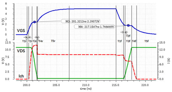
Figure 5.
Simulated switching waveforms of , , and in a capacitance-limited case.
The calculation (Cal.) and simulation (Sim.) results of the duration of each switching interval are shown in Table 4, in which the calculation result is based on the equations in Table 1.
Table 4.
Calculation and simulation results of switching interval duration.
The solution of Table 1 and the calculation result of Table 4 are accurate to the first-order. Compared with the simulation result, the accuracy of the calculation result of each interval in Table 4 is generally satisfactory with the exceptions of , , and . The duration of is particularly small compared with other intervals. The time constant of this interval is since the MOSFET is now in the ON state. The MOSFET is also in the ON state during , but the ending of is marked by when falls to . Moreover, goes through a substantial change in , but both and only change a little in . The errors of and come from the first-order linear approximation. During , and vary simultaneously. It is better to use a quadratic function for the approximation [32].
Figure 6 shows the switching waveform of , , and with a partially clamped current load ( nH). Now, the drain voltage changes faster than the drain current, and there is no Miller voltage in the turn-on process, which also means that this is an inductance-limited case. Instead, we can use to obtain an approximate (1.52 V) to calculate and , which were 195 ps and 575 ps, respectively. Compared with the simulated data (203 ps and 687 ps, respectively) in Figure 6, the relatively larger error of also comes from the first-order linear approximation. As was analyzed earlier, during of the turn-off sequence, must rise above to discharge . Using (12), the calculated was 1.30 nS, which is also an accurate value according to the simulated result in Figure 6.
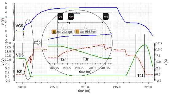
Figure 6.
Simulated switching waveforms of , , and in an inductance-limited case.
4.3. Verification of Analyzing Switching Loss
In this part, the simulation result of the switching loss was still based on the power MOSFET written in Verilog-A, and the circuit parameters were the same as in the preceding subsection. The simulated turn-on and turn-off switching losses were calculated by integrating over the switching time directly.
Using the above circuit parameters, the loss model in (13), which uses the traditional Miller plateau, the loss model in (14), which uses the proposed new Miller plateau (denoted by Proposed Model 1), and the loss model in (15), which uses the proposed new Miller plateau and further takes the gate current’s variation into account (denoted by Proposed Model 2), were calculated and compared. These three models were based on the loss calculation method in [30]. The Proposed Model 1 and Proposed Model 2 here do not indicate specific loss models, and they can be developed by other loss calculation methods only if the traditional Miller plateau is replaced by the proposed new Miller plateau, and the effect of the gate current’s variation was further included for the Proposed Model 2. For example, the corresponding Proposed Model 1 and Proposed Model 2 using the loss calculation method in [20] were also calculated and compared to the original piecewise-linear model in [20]. The aim was to verify the improvement of the prediction accuracy by replacing the traditional Miller plateau with the proposed new Miller plateau.
Figure 7a,b shows the curves of the turn-on and turn-off switching losses as a function of the load current for the Verilog-A simulation, the original Model in [20], the Proposed Model 1, and the Proposed Model 2, respectively. Based on the loss calculation method in [20], the Proposed Model 1 uses the new Miller plateau, while the original Model in [20] uses the conventional Miller plateau. As Table 5 shows, replacing the conventional Miller plateau by the new Miller plateau can improve the prediction accuracy of the switching loss: the average relative error of the Proposed Model 1 was almost reduced to 1/3 of the average relative error of the original Model in [20]. The Proposed Model 2, which further takes the gate current’s variation into account, had the smallest prediction error.
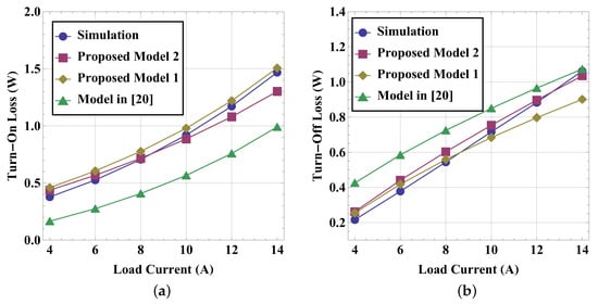
Figure 7.
Switching loss of the models based on [20] at 10 MHz, 10 V input voltage, and 5 V gate driving voltage: (a) turn-on loss as a function of load current; (b) turn-off loss as a function of load current.
Table 5.
The average relative error of different loss models based on two calculation methods when the load current changes from 4.0 A to 14 A at 10 MHz, 10 V input voltage, and 5 V gate driving voltage.
Figure 8a,b shows the curves of the turn-on and turn-off switching losses as a function of the gate driving voltage for the Verilog-A simulation, the original Model in [20], the Proposed Model 1, and the Proposed Model 2, respectively. As Table 6 shows, compared with the loss model based on conventional Miller plateau, the loss model based on new Miller plateau again better followed the trend of the simulation result: the average relative error of the Proposed Model 1 was almost reduced to 1/4 of the average relative error of the original Model in [20]; the Proposed Model 2, which further takes the gate current’s variation into account, had the smallest prediction error.
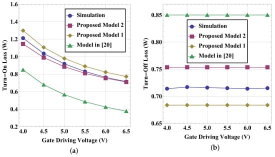
Figure 8.
Switching loss of the models based on [20] at 10 MHz, 10 V input voltage, and 10 A load current: (a) turn-on loss as a function of gate driving voltage; (b) turn-off loss as a function of gate driving voltage.
Table 6.
The average relative error of different loss models based on two calculation methods when the gate driving voltage changes from 4.0 V to 6.5 V at 10 MHz, 10 V input voltage, and 10 A load current.
Figure 9a,b shows the curves of the turn-on and turn-off switching losses as a function of the load current for the Verilog-A simulation, the original Model in [30], the Proposed Model 1, and the Proposed Model 2, respectively. Based on the loss calculation method in [30], the Proposed Model 1 uses the new Miller plateau, while the original Model in [30] uses the conventional Miller plateau. As Table 5 shows, replacing the conventional Miller plateau by the new Miller plateau can improve the prediction accuracy of the switching loss: the average relative error of the Proposed Model 1 was almost reduced to 1/3 of the average relative error of the original Model in [30]. The Proposed Model 2, which further takes the gate current’s variation into account, had the smallest prediction error: the average relative error is within 5.5%.
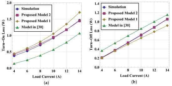
Figure 9.
Switching loss of the models based on [30] at 10 MHz, 10 V input voltage, and 5 V gate driving voltage: (a) turn-on loss as a function of load current; (b) turn-off loss as a function of load current.
Figure 10a,b shows the curves of the turn-on and turn-off switching losses as a function of the gate driving voltage for the Verilog-A simulation, the original Model in [30], the Proposed Model 1, and the Proposed Model 2, respectively. As Table 6 shows, compared with the loss model based on conventional Miller plateau, the loss model based on new Miller plateau again better followed the trend of the simulation result: the average relative error of the Proposed Model 1 was almost reduced to 1/2 of the average relative error of the original Model in [30]; the Proposed Model 2, which further takes the gate current’s variation into account, had the smallest prediction error and its average relative error is within 4.5%.
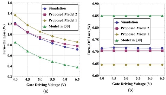
Figure 10.
Switching loss of the models based on [30] at 10 MHz, 10 V input voltage, and 10 A load current: (a) turn-on loss as a function of gate driving voltage; (b) turn-off loss as a function of gate driving voltage.
5. Conclusions
In order to estimate the switching loss of SMPS accurately, the relationship between the Miller plateau voltage and the displacement currents through parasitic capacitance of a power MOSFET was analyzed and a quantitative model was derived in this paper. Based on the proposed model, the Miller plateau should have different voltage levels during turn-on/-off, and it also changes according to different load conditions. Using the new Miller plateau, the switching waveform and switching loss can be analyzed and calculated more accurately. Experiment and simulation were performed to verify the proposed new Miller plateau and its use in analyzing switching process. For switching loss prediction, the benchmarking table shows that the achieved average relative error of the proposed Miller plateau-based loss model (Model 1) can be reduced to well below 10%, which is a 50∼75% reduction of the one obtained by the traditional Miller plateau-based model. Moreover, the error can be further reduced to around 5%, the lowest among these loss models, by using the proposed Miller plateau-based model (Model 2), taking into consideration the gate current’s variation. The proposed new Miller plateau can be further used to measure the device performance and to help to select the right device and gate driver for designing a high-frequency SMPS.
Author Contributions
Conceptualization, S.L. and S.S.; methodology, S.L., H.C., and M.Z.; software, S.L. and S.S.; validation, S.L., X.W., and M.Z.; formal analysis, S.L., N.X., and S.S.; writing—original draft preparation, S.L.; writing—review and editing, S.L., S.S., N.X., H.C., X.W., and M.Z. All authors read and agreed to the published version of the manuscript.
Funding
This research was supported by the Shanghai Municipal Science and Technology Major Project (Grant No. 2019SHZDZX01).
Data Availability Statement
All data, models, and code generated or used during the study appear in the submitted article.
Conflicts of Interest
The authors declare no conflict of interest.
Abbreviations
The following abbreviations are used in this manuscript:
| CMOS | Complementary metal-oxide semiconductor |
| DC | Direct current |
| EMI | Electromagnetic interference |
| FOM | Figures of merit |
| KCL | Kirchhoff’s current law |
| IoT | Internet of Things |
| MOSFET | Metal-oxide-semiconductor field-effect transistor |
| SMPS | Switching mode power supply |
| SPICE | Simulation Program with Integrated Circuit Emphasis |
Nomenclature
| , , | Parasitic interelectrode (gate, drain, and source) capacitances |
| External capacitance connected between the gate and source electrodes | |
| External capacitance connected between the drain and source electrodes | |
| Input capacitance. Equals | |
| Reverse transfer capacitance. Equals | |
| Output capacitance. Equals | |
| Switching frequency of an SMPS | |
| Power MOSFET’s transconductance in the ACTIVE state | |
| , , | Channel current, drain current, and load current |
| , | Miller plateau currents in the turn-on and turn-off processes |
| Average gate current when changes from to during turn-on | |
| Average gate current when changes from to during turn-off | |
| The constant rate when falls linearly from to zero during turn-on | |
| The constant rate when rises linearly from zero to during turn-off | |
| , | Parasitic inductances of the drain and source leads |
| , | Turn-on and turn-off switching power losses |
| Drain–source on-state resistance | |
| Gate resistance | |
| Switching period of an SMPS | |
| , | Turn-off time and turn-on time |
| to | Each interval of the turn-off sequence |
| to | Each interval of the turn-on sequence |
| The time constant related to and | |
| The time constant related to and | |
| , , | Gate–source voltage, gate–drain voltage, and drain–source voltage |
| Gate driving voltage | |
| Traditional Miller plateau voltage | |
| , | Miller plateau voltages in the turn-on and turn-off processes |
| Power MOSFET’s threshold voltage |
References
- Minoli, D.; Sohraby, K.; Occhiogrosso, B. IoT Considerations, Requirements, and Architectures for Smart Buildings—Energy Optimization and Next-Generation Building Management Systems. IEEE J. Internet Things 2017, 4, 269–283. [Google Scholar] [CrossRef]
- Chettri, L.; Bera, R. A Comprehensive Survey on Internet of Things (IoT) Toward 5G Wireless Systems. IEEE J. Internet Things 2020, 7, 16–32. [Google Scholar] [CrossRef]
- Shousha, M.; Dinulovic, D.; Haug, M.; Petrovic, T.; Mahgoub, A. A Power Management System for Electromagnetic Energy Harvesters in Battery/Batteryless Applications. IEEE J. Emerg. Sel. Top. Power Electron. 2020, 8, 3644–3657. [Google Scholar] [CrossRef]
- Ruan, T.; Chew, Z.J.; Zhu, M. Energy-Aware Approaches for Energy Harvesting Powered Wireless Sensor Nodes. IEEE J. Sens. 2017, 17, 2165–2173. [Google Scholar] [CrossRef]
- Perreault, D.J.; Hu, J.; Rivas, J.M.; Han, Y.; Leitermann, O.; Pilawa-Podgurski, R.C.N.; Sagneri, A.; Sullivan, C.R. Opportunities and Challenges in Very High Frequency Power Conversion. In Proceedings of the 2009 Twenty-Fourth Annual IEEE Applied Power Electronics Conference and Exposition (APEC), Washington, DC, USA, 15–19 February 2009; pp. 1–14. [Google Scholar]
- Huang, C.; Mok, P.K.T. An 84.7% Efficiency 100-MHz Package Bondwire-Based Fully Integrated Buck Converter with Precise DCM Operation and Enhanced Light-Load Efficiency. IEEE J. Solid-State Circuits 2013, 48, 2595–2607. [Google Scholar] [CrossRef]
- Lee, B.; Song, M.K.; Maity, A.; Ma, D.B. A 25-MHz Four-Phase SAW Hysteretic Control DC-DC Converter with 1-Cycle Active Phase Count. IEEE J. Solid-State Circuits 2019, 54, 1755–1763. [Google Scholar] [CrossRef]
- Liu, X.; Huang, C.; Mok, P.K.T. A High-Frequency Three-Level Buck Converter with Real-Time Calibration and Wide Output Range for Fast-DVS. IEEE J. Solid-State Circuits 2018, 53, 582–595. [Google Scholar] [CrossRef]
- Dai, J.; Zhao, J.; Qu, K.; Lin, M. A Fast Hysteresis Control Strategy Based on Capacitor Charging and Discharging. IEICE Electron. Express 2014, 11, 1–6. [Google Scholar] [CrossRef][Green Version]
- Shenoy, P.S.; Amaro, M.; Morroni, J.; Freeman, D. Comparison of a Buck Converter and a Series Capacitor Buck Converter for High-Frequency, High-Conversion-Ratio Voltage Regulators. IEEE Trans. Power Electron. 2016, 31, 7006–7015. [Google Scholar] [CrossRef]
- Xu, D.; Guan, Y.; Wang, Y.; Wang, W. Topologies and Control Strategies of Very High Frequency Converters: A Survey. CPSS Trans. Power Electron. Appl. 2017, 2, 28–38. [Google Scholar] [CrossRef]
- Cheng, X.; Shao, W.; Zhang, Y.; Zeng, J.; Zhang, Z. High Frequency and High Efficiency DC-DC Converter with Sensorless Adaptive-Sizing Technique. IEICE Electron. Express 2020, 17, 1–4. [Google Scholar] [CrossRef]
- Zhao, Q.; Stojcic, G. Characterization of Cdv/dt Induced Power Loss in Synchronous Buck DC-DC Converters. IEEE Trans. Power Electron. 2007, 22, 1508–1513. [Google Scholar] [CrossRef]
- Wang, Q. The Impact of Parasitic Elements on Spurious Turn-on in Phase-Shifted Full-Bridge Converters. J. Power Electron. 2016, 16, 883–893. [Google Scholar] [CrossRef]
- Wang, J.; Chung, H.S. Impact of Parasitic Elements on the Spurious Triggering Pulse in Synchronous Buck Converter. IEEE Trans. Power Electron. 2014, 29, 6672–6685. [Google Scholar] [CrossRef]
- Li, R.; Zhu, J.; Xie, M. Parasitic Parameter Effects on the dv/dt-Induced Low-Side MOSFET False Turn-on in Synchronous Buck Converters. In Proceedings of the 2019 IEEE Applied Power Electronics Conference and Exposition (APEC), Anaheim, CA, USA, 17–21 March 2019; pp. 2247–2254. [Google Scholar]
- Liu, T.; Wong, T.T.Y.; Shen, Z.J. A Survey on Switching Oscillations in Power Converters. IEEE J. Emerg. Sel. Top. Power Electron. 2020, 8, 893–908. [Google Scholar] [CrossRef]
- Ren, Y.; Xu, M.; Zhou, J.; Lee, F.C. Analytical Loss Model of Power MOSFET. IEEE Trans. Power Electron. 2006, 21, 310–319. [Google Scholar]
- Funaki, T.; Arioka, H.; Hikihara, T. The Influence of Parasitic Components on Power MOSFET Switching Operation in Power Conversion Circuits. IEICE Electron. Express 2009, 6, 1697–1701. [Google Scholar] [CrossRef]
- Klein, J. Synchronous Buck MOSFET Loss Calculations with Excel Model; Application Note AN-6005; Fairchild Semiconductor. 2006. Available online: http://www.bdtic.com/DataSheet/FAIRCHILD/AN-6005.pdf (accessed on 18 August 2021).
- Depew, J. Efficiency Analysis of a Synchronous Buck Converter Using Microsoft Office Excel-Based Loss Calculator. Application Note AN-1471. Microchip Technology Inc. 2012. Available online: https://www.microchip.com/en-us/application-notes/an1471 (accessed on 18 August 2021).
- Lakkas, G. MOSFET Power Losses and How They Affect Power-Supply Efficiency. Application Note Slyt664. Texas Instruments. 2016. Available online: https://www.ti.com/lit/an/slyt664/slyt664.pdf (accessed on 18 August 2021).
- Rodriguez, M.; Rodriguez, A.; Miaja, P.F.; Sebastian, J. Analysis of the Switching Process of Power MOSFETs Using a New Analytical Losses Model. In Proceedings of the 2009 IEEE Energy Conversion Congress and Exposition (ECCE), San Jose, CA, USA, 20–24 September 2009; pp. 3790–3797. [Google Scholar]
- Eberle, W.; Zhang, Z.; Liu, Y.; Sen, P.C. A Practical Switching Loss Model for Buck Voltage Regulators. IEEE Trans. Power Electron. 2009, 24, 700–713. [Google Scholar] [CrossRef]
- Xiong, Y.; Sun, S.; Jia, H.; Shea, P.; Shen, Z.J. New Physical Insights on Power MOSFET Switching Losses. IEEE Trans. Power Electron. 2009, 24, 525–531. [Google Scholar] [CrossRef]
- Zhang, Z.; Fu, J.; Liu, Y.; Sen, P.C. Switching Loss Analysis Considering Parasitic Loop Inductance with Current Source Drivers for Buck Converters. In Proceedings of the 2010 Twenty-Fifth Annual IEEE Applied Power Electronics Conference and Exposition (APEC), Palm Springs, CA, USA, 21–25 February 2010; pp. 1482–1486. [Google Scholar]
- Castro, I.; Roig, J.; Gelagaev, R.; Vlachakis, B.; Bauwens, F.; Lamar, D.G.; Driesen, J. Analytical Switching Loss Model for Superjunction MOSFET with Capacitive Nonlinearities and Displacement Currents for DC-DC Power Converters. IEEE Trans. Power Electron. 2016, 31, 2485–2495. [Google Scholar] [CrossRef]
- Nikoo, M.S.; Jafari, A.; Perera, N.; Matioli, E. New Insights on Output Capacitance Losses in Wide-Band-Gap Transistors. IEEE Trans. Power Electron. 2020, 35, 6663–6667. [Google Scholar] [CrossRef]
- Yoo, A.; Chang, M.; Trescases, O.; Wang, H.; Ng, W.T. FOM (Figure of Merit) Analysis for Low Voltage Power MOSFETs in DC-DC Converter. In Proceedings of the 2007 IEEE Conference on Electron Devices and Solid-State Circuits (EDSSC), Tainan, Taiwan, 20–22 December 2007; pp. 1039–1042. [Google Scholar]
- Ying, Y. Device Selection Criteria Based on Loss Modeling and Figure of Merit. Master’s Thesis, Virginia Polytechnic Institute and State University, Blacksburg, VA, USA, 2008. [Google Scholar]
- Erickson, R.W.; Maksimovic, D. Fundamentals of Power Electronics, 2nd ed.; Kluwer Academic Publishers: New York, NY, USA, 2004; pp. 93–94. [Google Scholar]
- Grant, D.A.; Gowar, J. Power MOSFETs: Theory and Applications; John Wiley & Sons: New York, NY, USA, 1989; pp. 97–132. [Google Scholar]
- Zhang, H.; Zhao, M.; Wu, X. Zero-Current Switching Method for DC-DC Buck Converter in Portable Application. Electron. Lett. 2015, 51, 1913–1914. [Google Scholar] [CrossRef]
- Razavi, B. Design of Analog CMOS Integrated Circuits, 2nd ed.; McGraw-Hill Education: New York, NY, USA, 2017; pp. 174–178. [Google Scholar]
- Baker, R.J. CMOS: Circuit Design, Layout, and Simulation, 3rd ed.; John Wiley & Sons: Hoboken, NJ, USA, 2010; pp. 660–663. [Google Scholar]
- Sansen, W.M.C. Analog Design Essentials; Springer: Dordrecht, The Netherlands, 2006; pp. 214–215. [Google Scholar]
- NCE2030K. Datasheet: NCE N-Channel Enhanced Mode Power MOSFET (v1.0); NCE Power Co.: Wuxi, China; Available online: https://pdf1.alldatasheetcn.com/datasheet-pdf/view/982315/NCEPOWER/NCE2030K.html (accessed on 18 August 2021).


Publisher’s Note: MDPI stays neutral with regard to jurisdictional claims in published maps and institutional affiliations. |
© 2021 by the authors. Licensee MDPI, Basel, Switzerland. This article is an open access article distributed under the terms and conditions of the Creative Commons Attribution (CC BY) license (https://creativecommons.org/licenses/by/4.0/).