Author Contributions
Conceptualization, G.C.K., J.S., J.W.K., M.J.K. and G.D.; methodology, G.C.K.; validation, G.C.K.; formal analysis, G.C.K.; investigation, G.C.K., J.S., M.J.K. and J.A.A.; resources, J.W.K., M.J.K., J.A.A. and G.D.; writing—original draft preparation, G.C.K. and G.Z.; writing—review and editing, G.C.K., G.Z., J.S. and J.W.K.; supervision, J.S. and J.W.K.; project administration, J.W.K., M.J.K. and G.D.; funding acquisition, M.J.K. and G.D. All authors have read and agreed to the published version of the manuscript.
Figure 1.
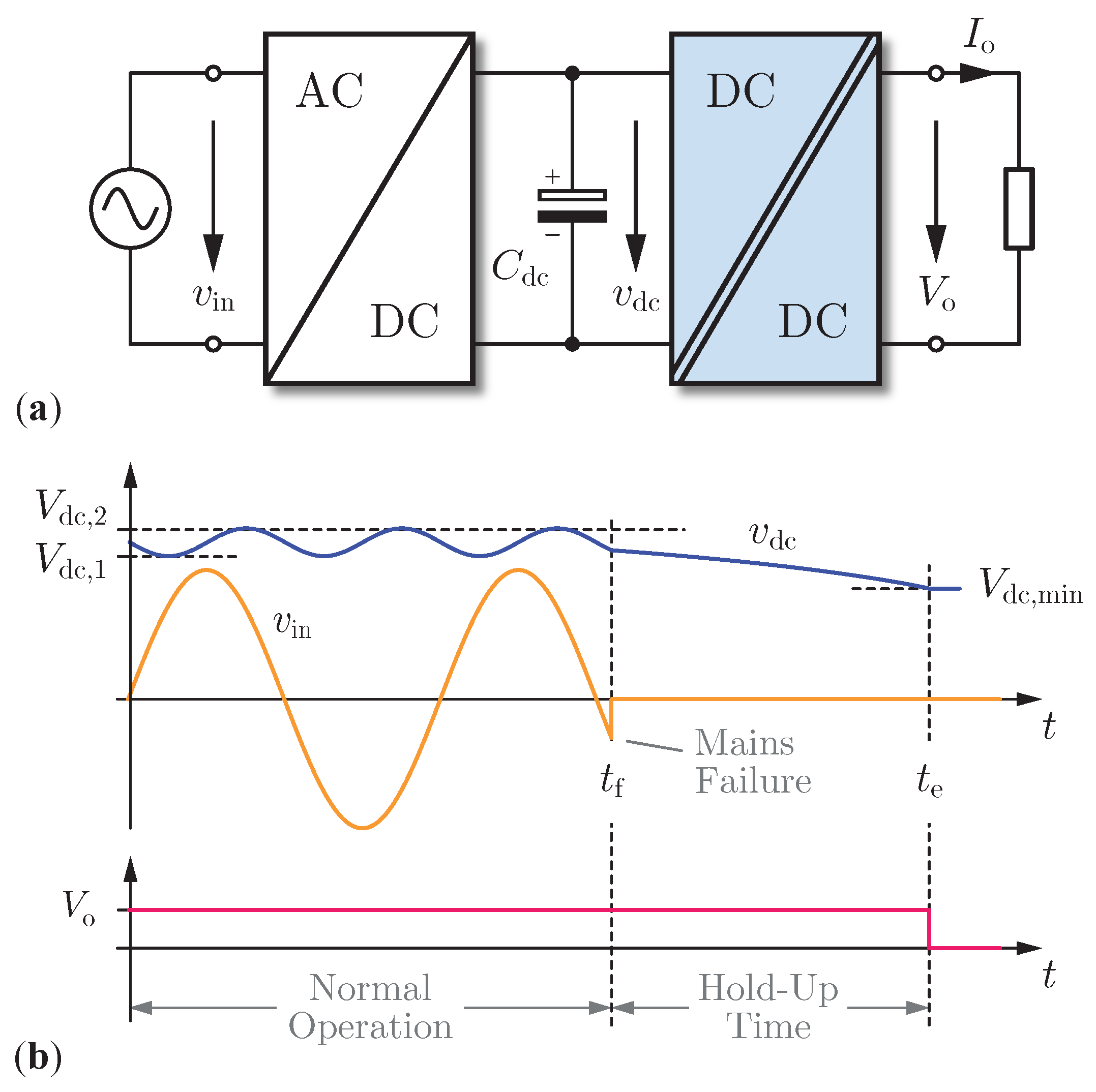
(a) Industrial power supply block diagram to convert AC-mains voltage to a high-current output; this work focused on the DC/DC converter. The requirements of the DC-link capacitor () are driven by the hold-up time requirements (here, ) during fault conditions, as shown in (b). Even with the input voltage range specified here (), the DC-link capacitor accounts for nearly 15% of the allocated system volume, indicating how critical this wide input range for the DC/DC converter is to overall system power density.
Figure 1.
(a) Industrial power supply block diagram to convert AC-mains voltage to a high-current output; this work focused on the DC/DC converter. The requirements of the DC-link capacitor () are driven by the hold-up time requirements (here, ) during fault conditions, as shown in (b). Even with the input voltage range specified here (), the DC-link capacitor accounts for nearly 15% of the allocated system volume, indicating how critical this wide input range for the DC/DC converter is to overall system power density.
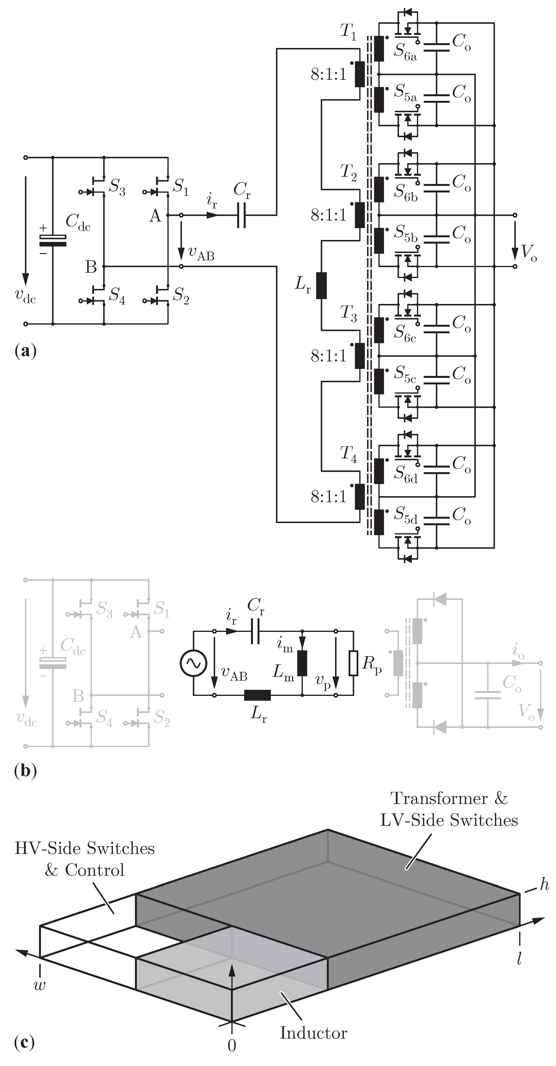
Figure 2.
(a) Power circuit of the proposed DC/DC converter featuring GaN devices for the primary-side full-bridge, power MOSFETs operating as synchronous rectifiers on the secondary-side, and a series-input, paralleled-output, center-tapped matrix transformer. The converter operates resonantly and has the simplified circuit shown in (b), where the fundamental-harmonic-approximation may be used to capture the fundamental component of switched waveforms. (c) Proposed layout with matrix transformer, synchronous rectifiers and output capacitors as the main block defining the converter’s width (w) and height (h), and the PCB inductor and primary-side full-bridge fixing the footprint’s length (l).
Figure 3.
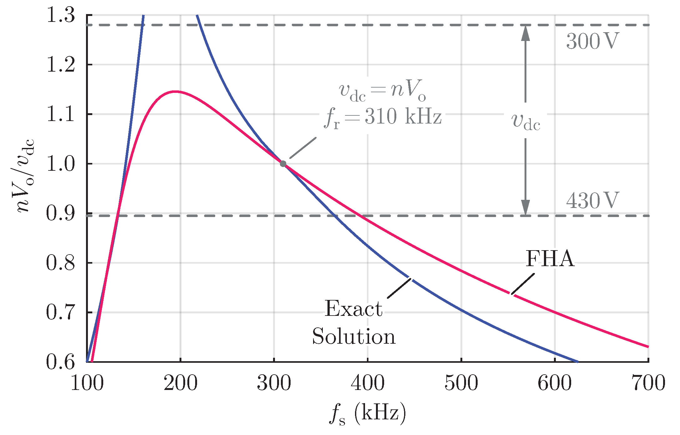
Graphical description of the output-to-input conversion ratio (normalized by the transformer turns ratio
n) as a function of the switching frequency (control variable). The exact solution, obtained through circuit simulation, is compared to the fundamental-harmonic-approximation (FHA), where we see that the the FHA captures the correct monotonic behavior of the gain function. For the given
range (300
–430
) and the parameters selected in
Section 2.1, the converter operates from 210
to 350
.
Figure 3.
Graphical description of the output-to-input conversion ratio (normalized by the transformer turns ratio
n) as a function of the switching frequency (control variable). The exact solution, obtained through circuit simulation, is compared to the fundamental-harmonic-approximation (FHA), where we see that the the FHA captures the correct monotonic behavior of the gain function. For the given
range (300
–430
) and the parameters selected in
Section 2.1, the converter operates from 210
to 350
.
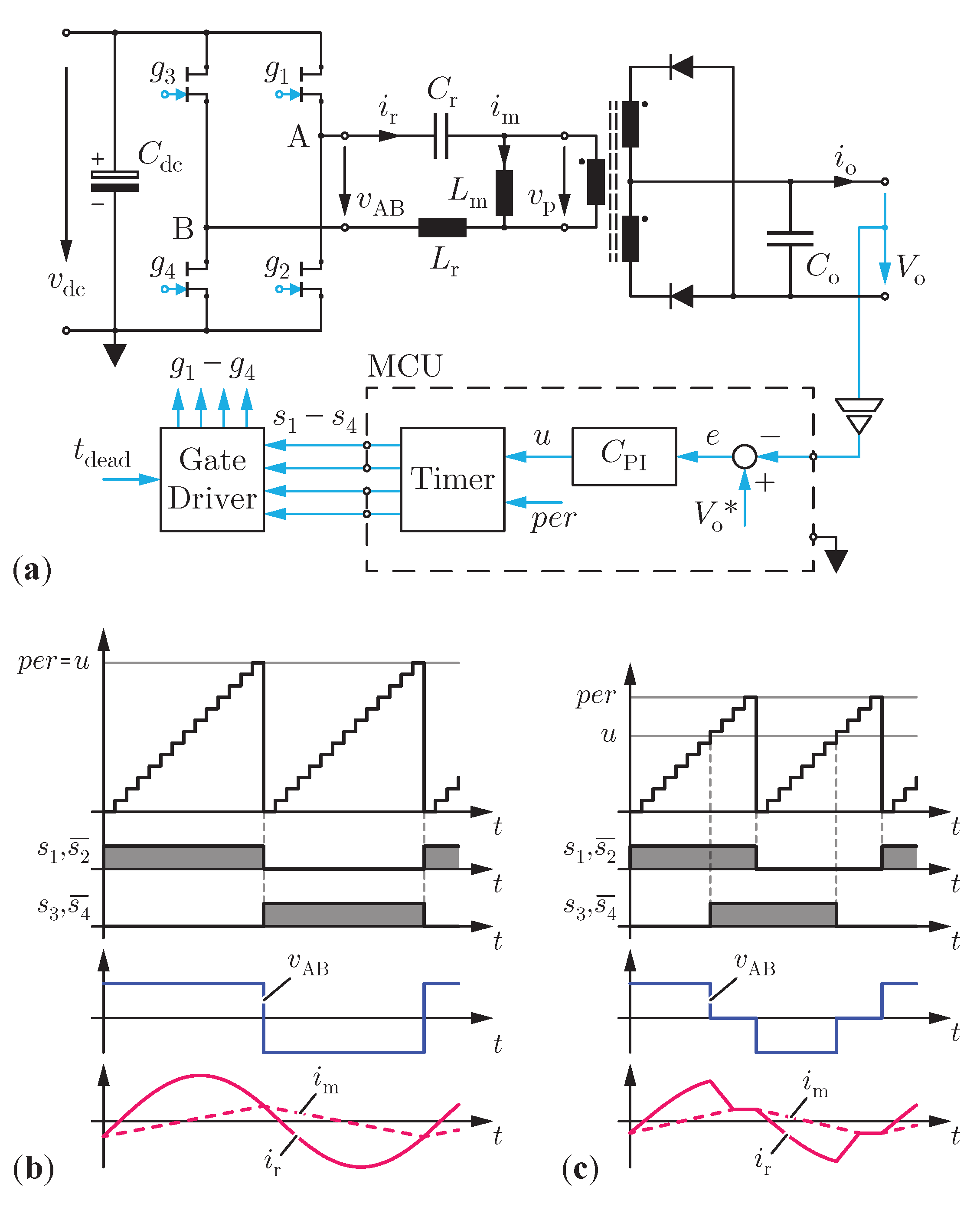
Figure 4.
(a) Proposed control topology for the DC/DC converter, with output-voltage regulation by variable frequency using only an isolated low-voltage measurement and a low-cost, 32-pin ST Arm Cortex M4 as the MCU. (b) Continuous conduction mode (CCM) operation, where the digital PI controller adjusts the period of the MCU timer to trigger . (c) When the control variable (u) is lower than the minimum (user-defined) switching period (), the converter enters discontinuous conduction mode (DCM), with a fixed frequency and a variable phase-shift to control the output voltage to the reference value (*).
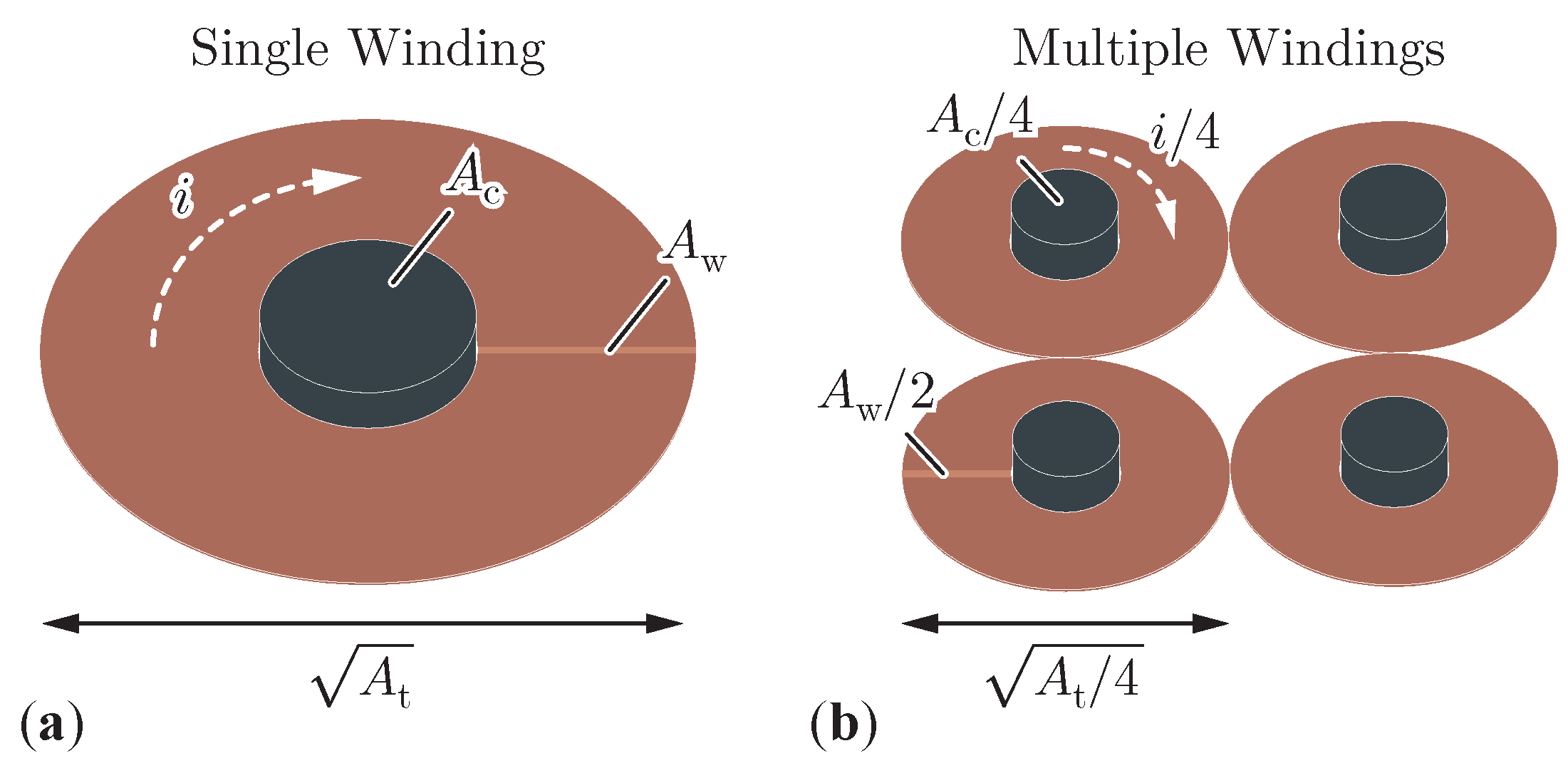
Figure 5.
(a) Illustrative scheme of a PCB-integrated, single-turn secondary-side winding with window area, core cross-section area, total footprint area, and current i. (b) Winding-loss minimization at the expense of increased core loss by means of a multi-output (matrix) structure with paralleled windings that reduces the current density by a factor of 2 for a fixed total footprint area and fixed current i.
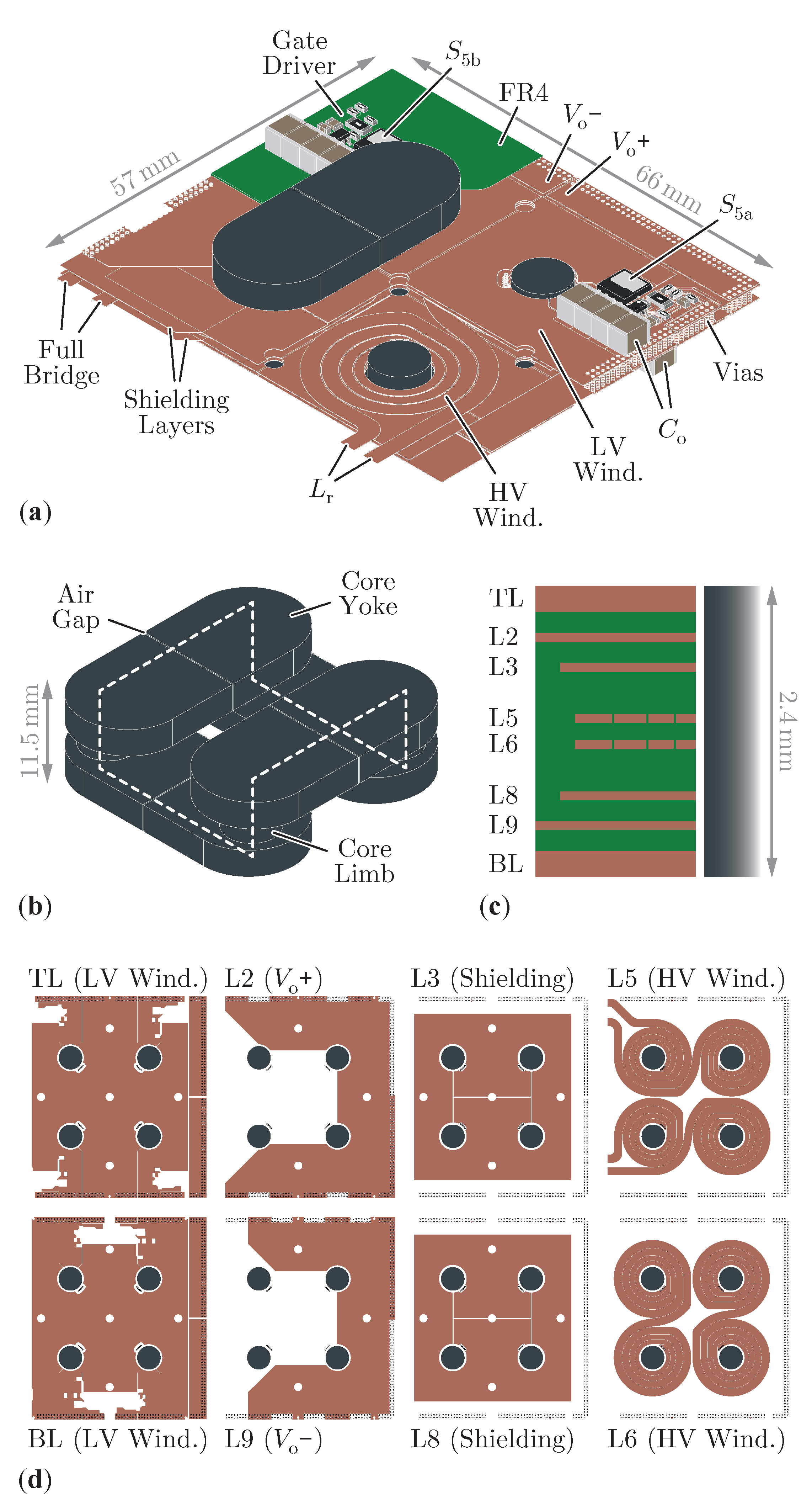
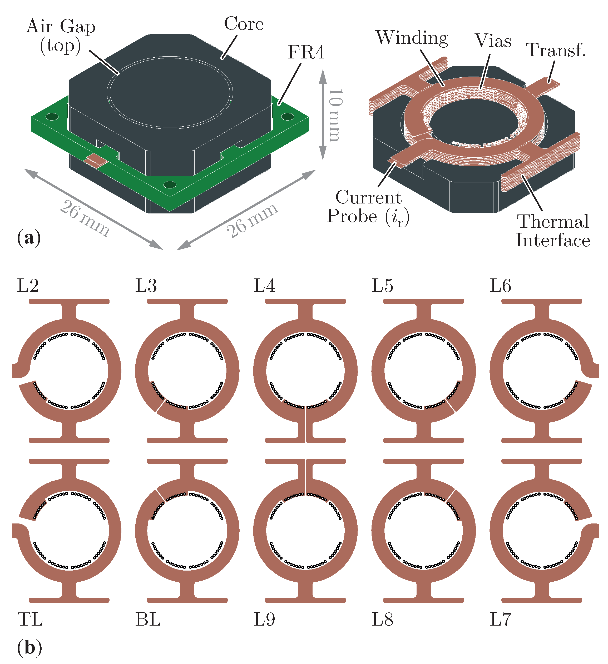
Figure 6.
(a) The 3-D view of the snake-core matrix transformer with cutaway view of the PCB-integrated windings. The secondary-side semiconductors and output capacitors are placed directly above the low-voltage windings for low termination losses and minimization of commutation loops. (b) Snake core with the single path for magnetic flux highlighted with white dashed lines. (c) PCB layer stackup from the top (TL) to bottom layer (BL), with copper and isolation thicknesses proportional to the final design. (d) Layer-by-layer copper of the 10-layer layout, with layers L4/L7 empty to reduce parasitic capacitance.
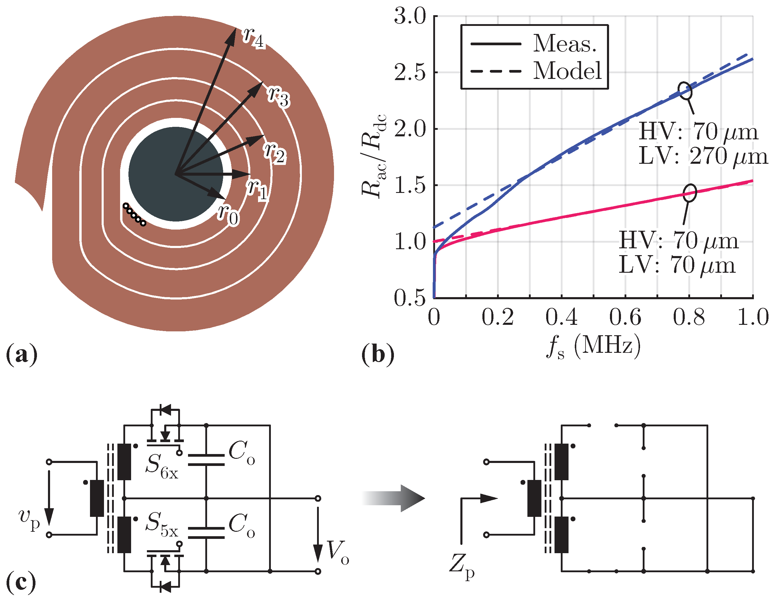
Figure 7.
(
a) Radii calculated from (
10) for minimizing winding resistance. (
b) Transformer AC-to-DC resistance ratio across frequency—measured as shown in (
c)—with secondary-side short-circuited for two copper-thickness arrangements: 70
primary (HV) and 70
secondary-side (LV) windings, or 70
HV and 270
LV windings (with
copper foils soldered onto the 70
LV windings for experimental results). (
c) Measurement technique for transformer resistance measurements, with measurement opens and shorts highlighted at right.
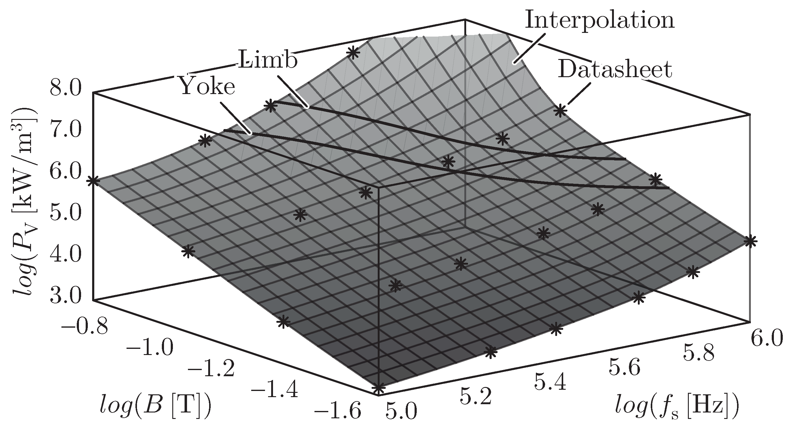
Figure 8.
N49-ferrite hysteric losses (volumetric) as a function of flux density and frequency (axes in log scale). Stars are datasheet-given values, which are interpolated as inputs into continuous loss models. The frequency-dependent limb and yoke fluxes are calculated using (
8) and shown with black lines on the top of the interpolation surface, indicating that core losses will decrease at higher operating frequencies due to the lower flux density.
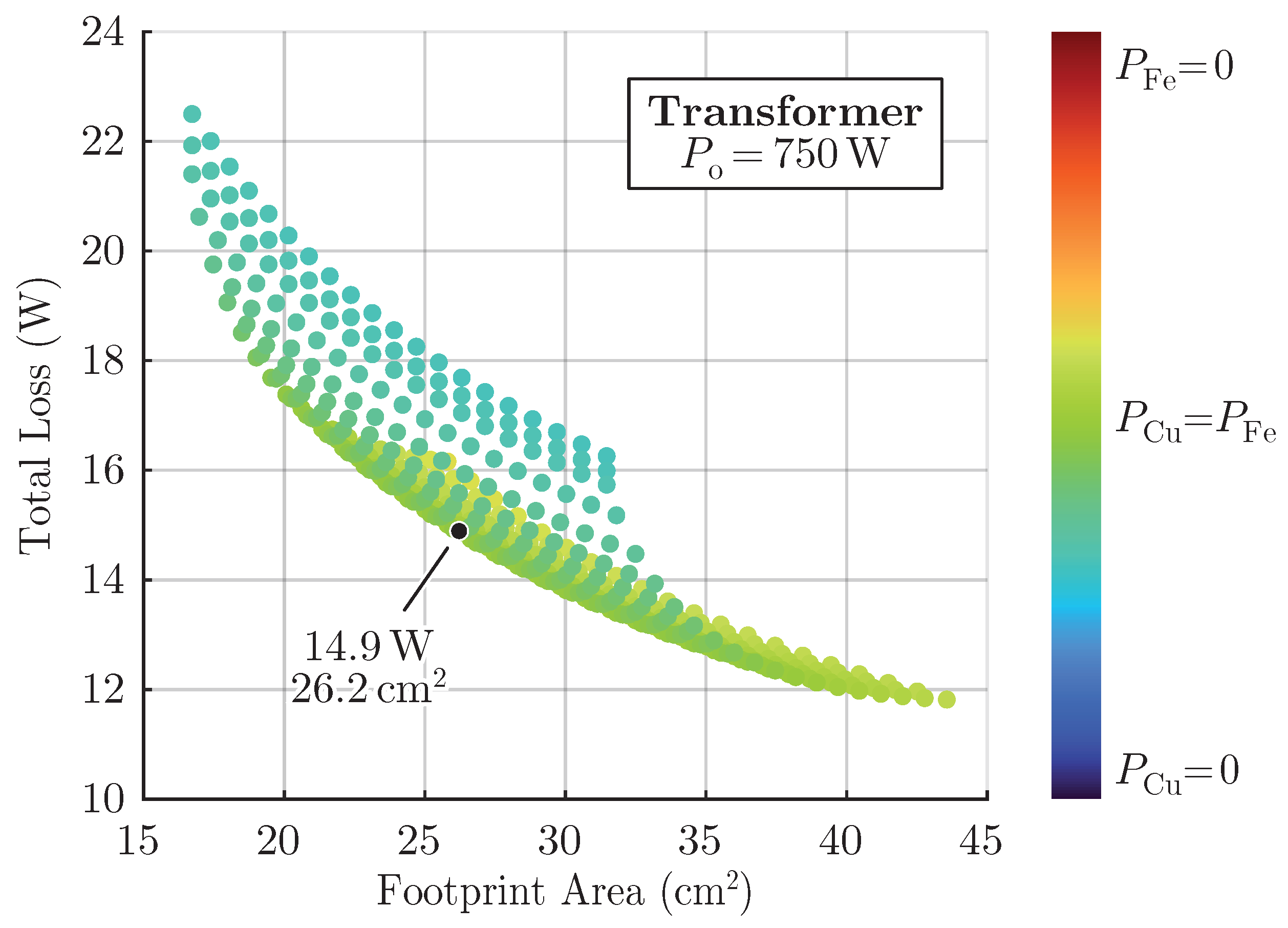
Figure 9.
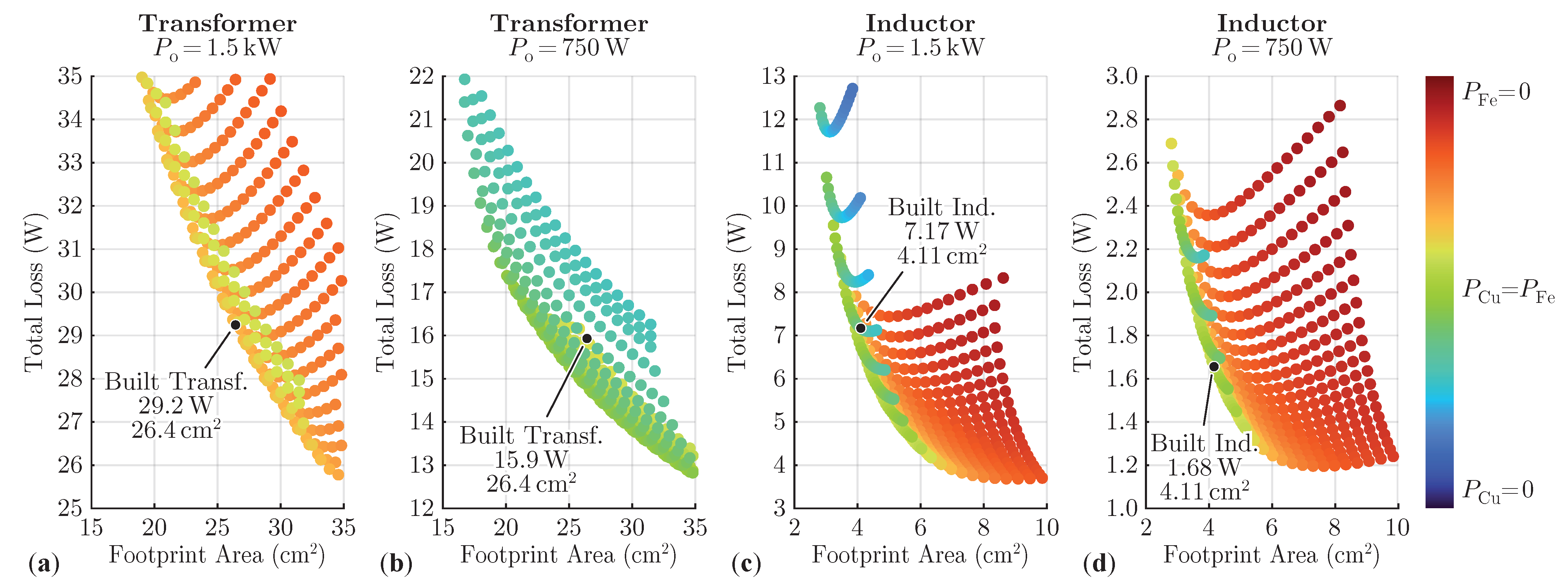
Pareto optimizations between total loss—sum of copper (
) and core (
) losses—and footprint area (directly related to volume) of the PCB-integrated (
a,
b) transformer and (
c,
d) inductor for (
a,
c) nominal and (
b,
d) 50% load. The design spaces were defined by sweeping core radius and winding width values for each of the two components to trade off the winding and core area. Selected designs that were Pareto-optimized for nominal load (
) are shown as black dots, with the design characteristics of
Table 4. Note that the Pareto-optimal designs are constant between full and 50% load for the inductor but change significantly for the transformer.
Figure 9.
Pareto optimizations between total loss—sum of copper (
) and core (
) losses—and footprint area (directly related to volume) of the PCB-integrated (
a,
b) transformer and (
c,
d) inductor for (
a,
c) nominal and (
b,
d) 50% load. The design spaces were defined by sweeping core radius and winding width values for each of the two components to trade off the winding and core area. Selected designs that were Pareto-optimized for nominal load (
) are shown as black dots, with the design characteristics of
Table 4. Note that the Pareto-optimal designs are constant between full and 50% load for the inductor but change significantly for the transformer.
Figure 10.
(
a) The 3-D view of the primary-side inductor (
) with PCB-integrated windings schematically shown with cutaways. Winding heat is transferred by thermal interfaces to adjacent surfaces that can be thermally coupled to heat sinks for cooling. Following [
25], air gaps are strategically placed above and underneath the windings to improve current distribution and boost efficiency. (
b) Layer-by-layer copper of the 10-layer stackup.
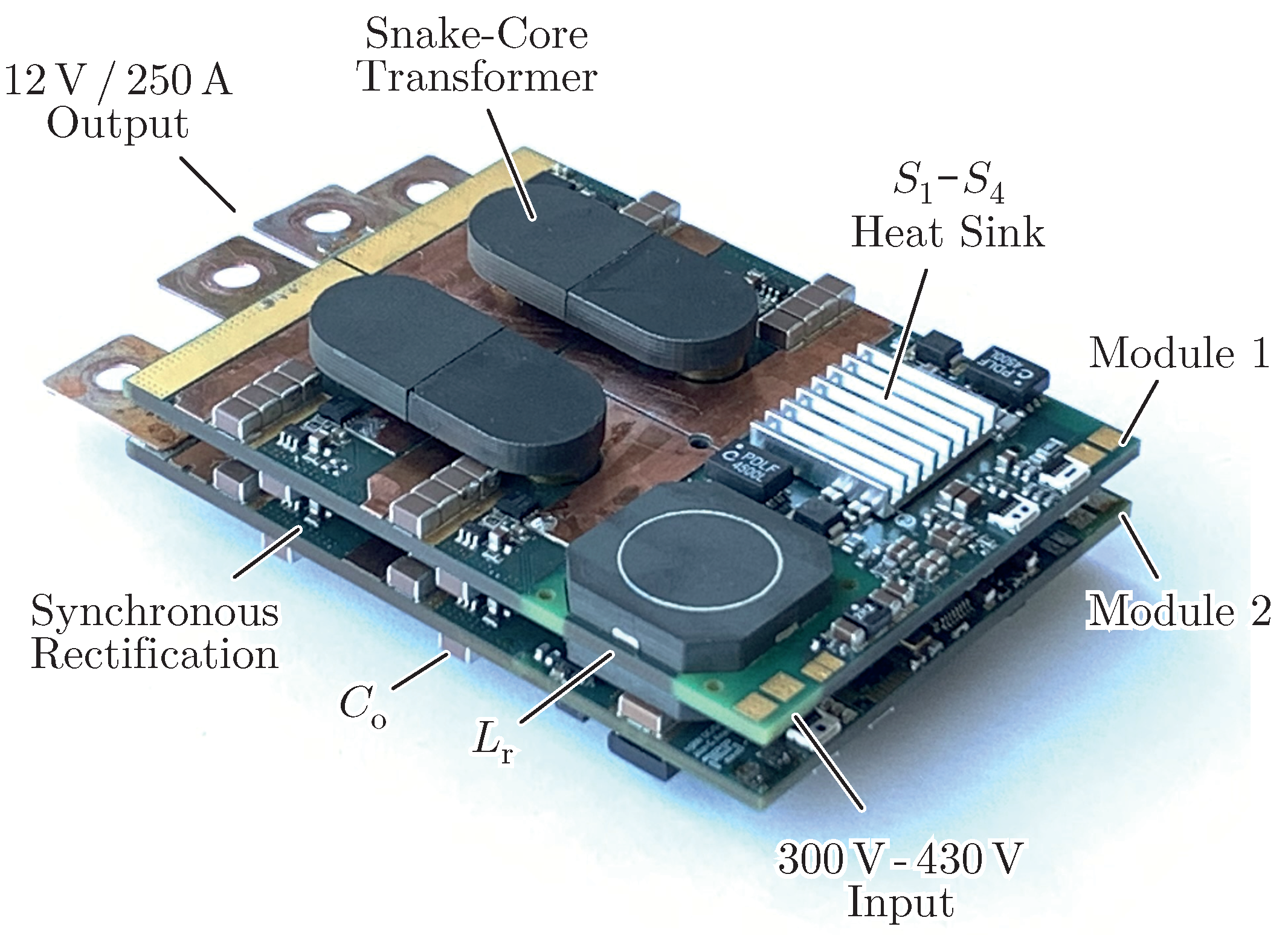
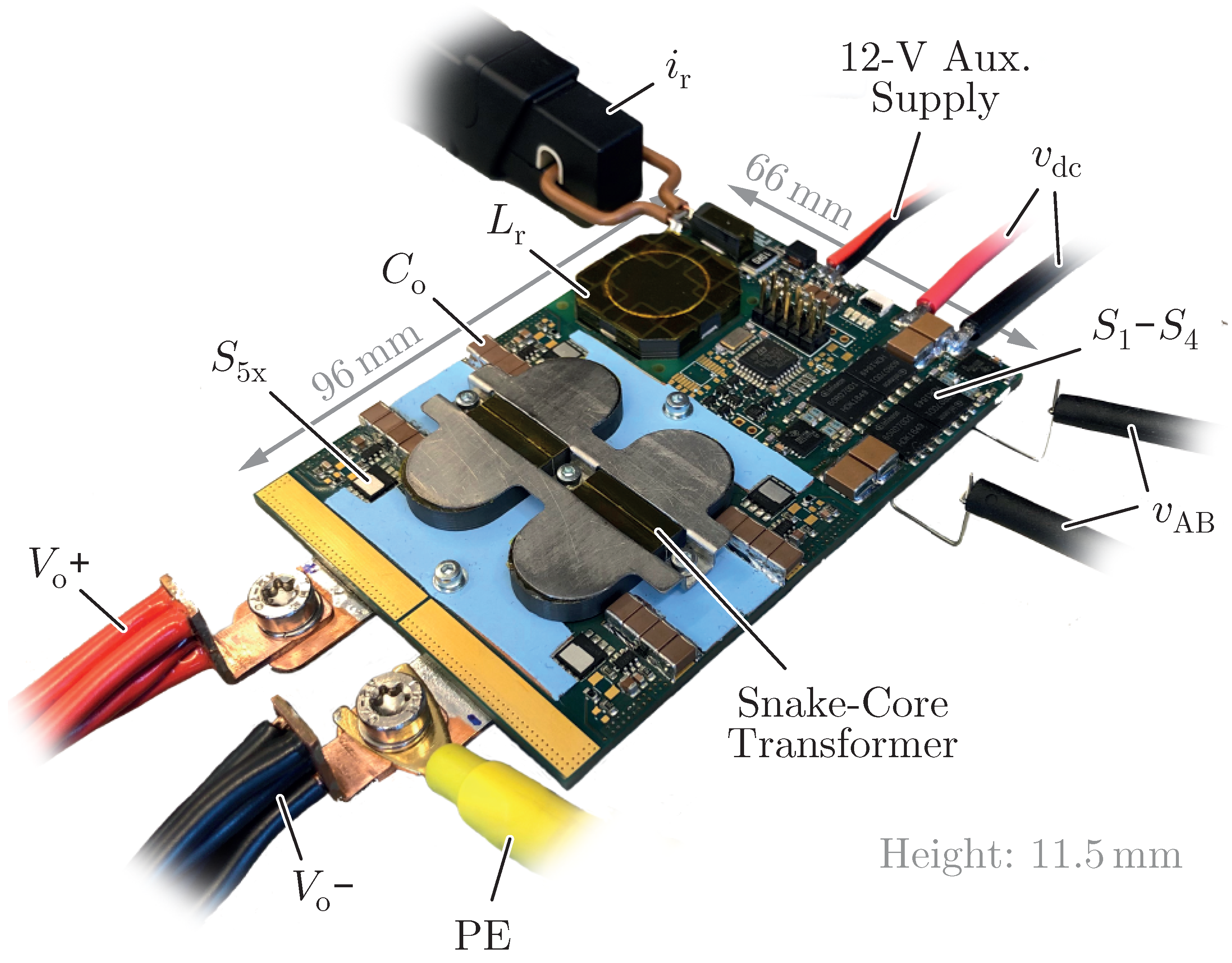
Figure 11.
The
hardware demonstrator of the DC/DC resonant converter, measuring 96
× 66
×
. Key components and measurement devices are highlighted, with key values and implementations given in
Table 6.
Figure 11.
The
hardware demonstrator of the DC/DC resonant converter, measuring 96
× 66
×
. Key components and measurement devices are highlighted, with key values and implementations given in
Table 6.
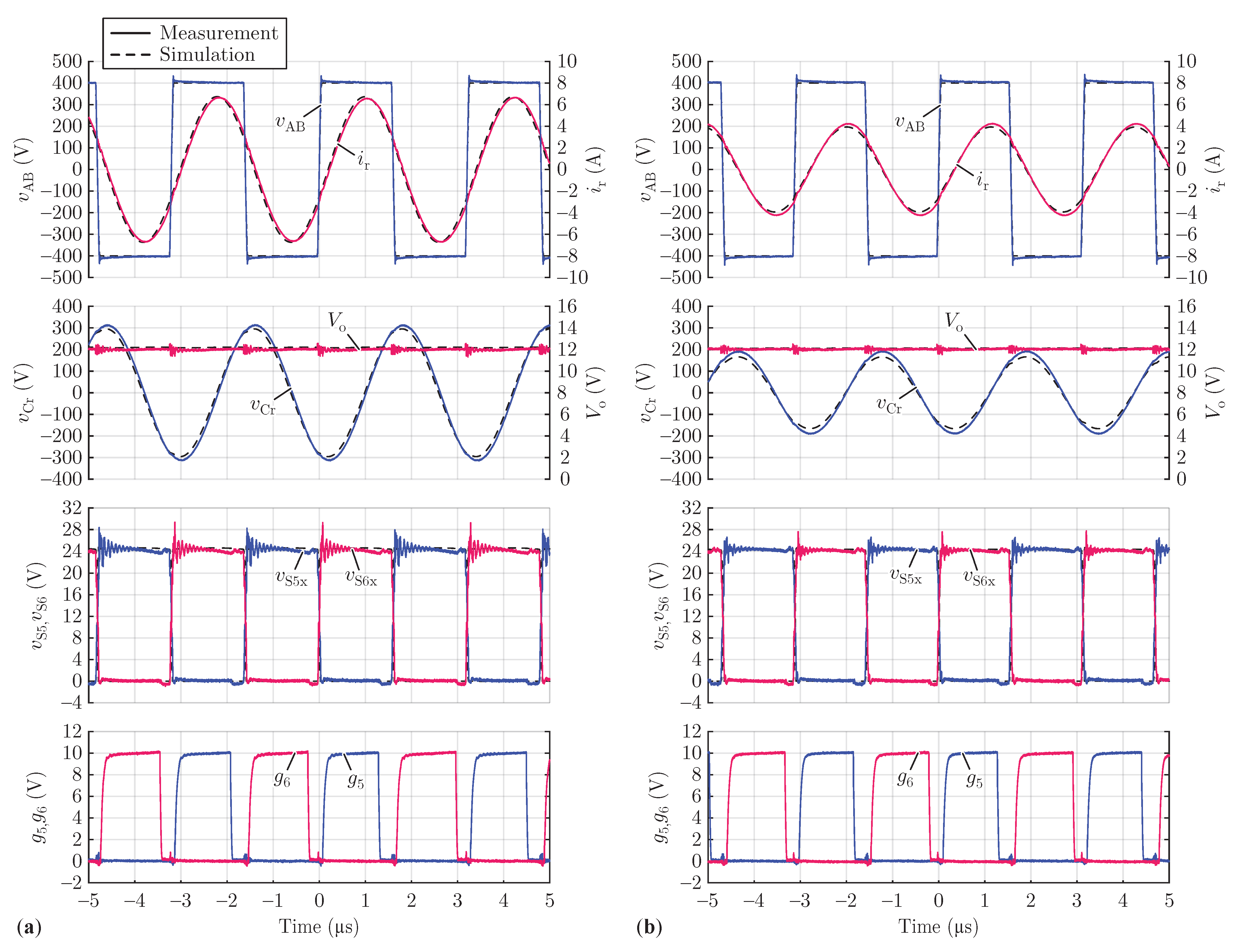
Figure 12.
Key operating waveforms captured at (a) nominal and (b) 50% load, demonstrating good agreement with circuit-simulation data (shown as dashed lines). Output voltage () is regulated at 12 by controlling the switching frequency of . The sinusoidal shape of minimizes harmonic losses, and synchronous rectification supports both ZVS and ZCS of the LV-side switches (drain-to-source voltages / commute naturally at zero current) and reduces body-diode losses by conducting most of the current through the MOSFET channel (gate signals / are commanded after and before switching actions).
Figure 13.
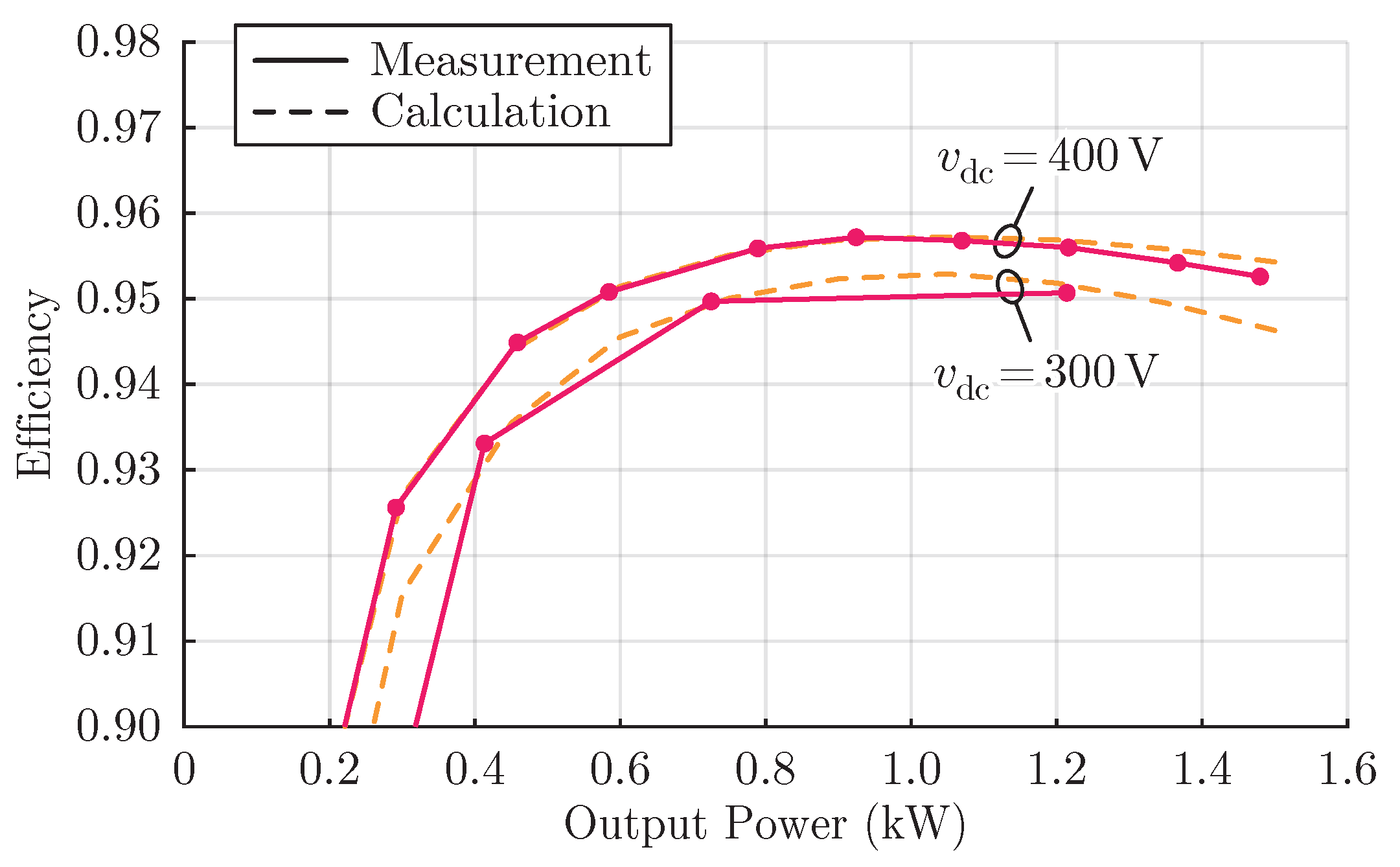
DC/DC calculated and electrically-measured efficiencies from input () to output () at different load conditions and two input voltages, including all loss components.
Figure 13.
DC/DC calculated and electrically-measured efficiencies from input () to output () at different load conditions and two input voltages, including all loss components.
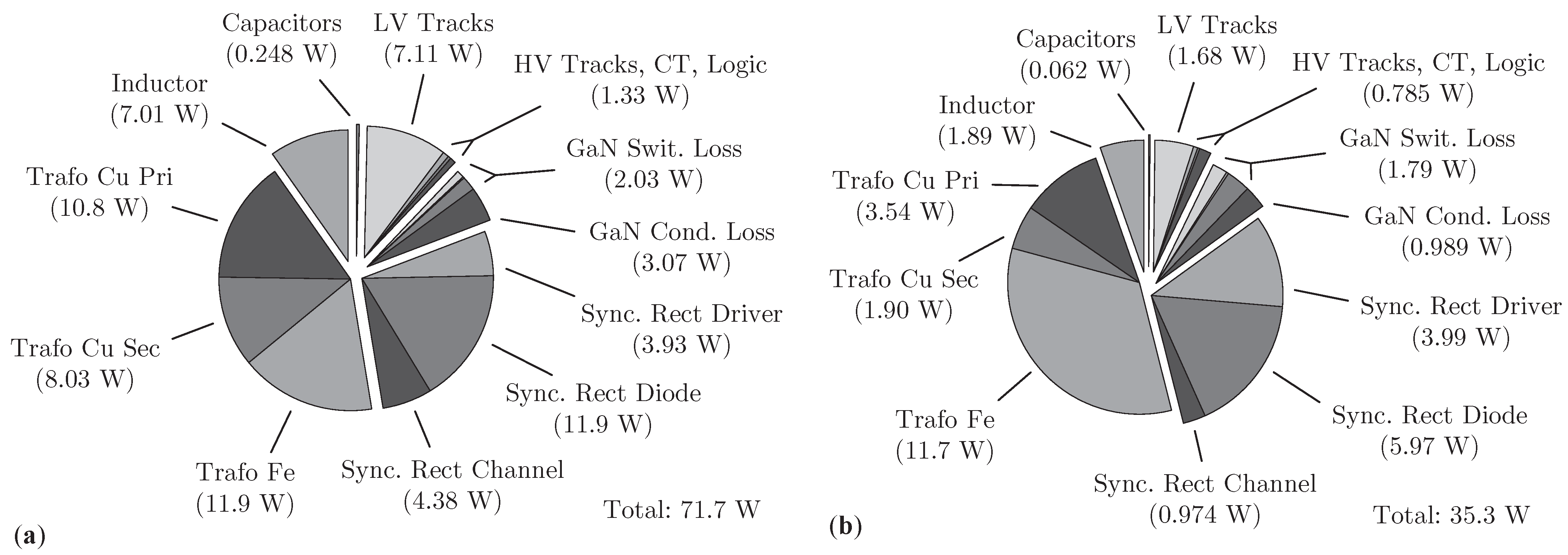
Figure 14.
(a) Full- and (b) 50%-load loss budgets for the DC/DC converter with and . Transformer, synchronous rectifiers and HV-side components/PCB tracks represent the three groups of loss contributors. Transformer losses accounts for 43% and 49% of the total losses at full and 50% load, respectively. Synchronous rectification is the second element with highest loss, achieving nearly 30% of the total losses in both load conditions.
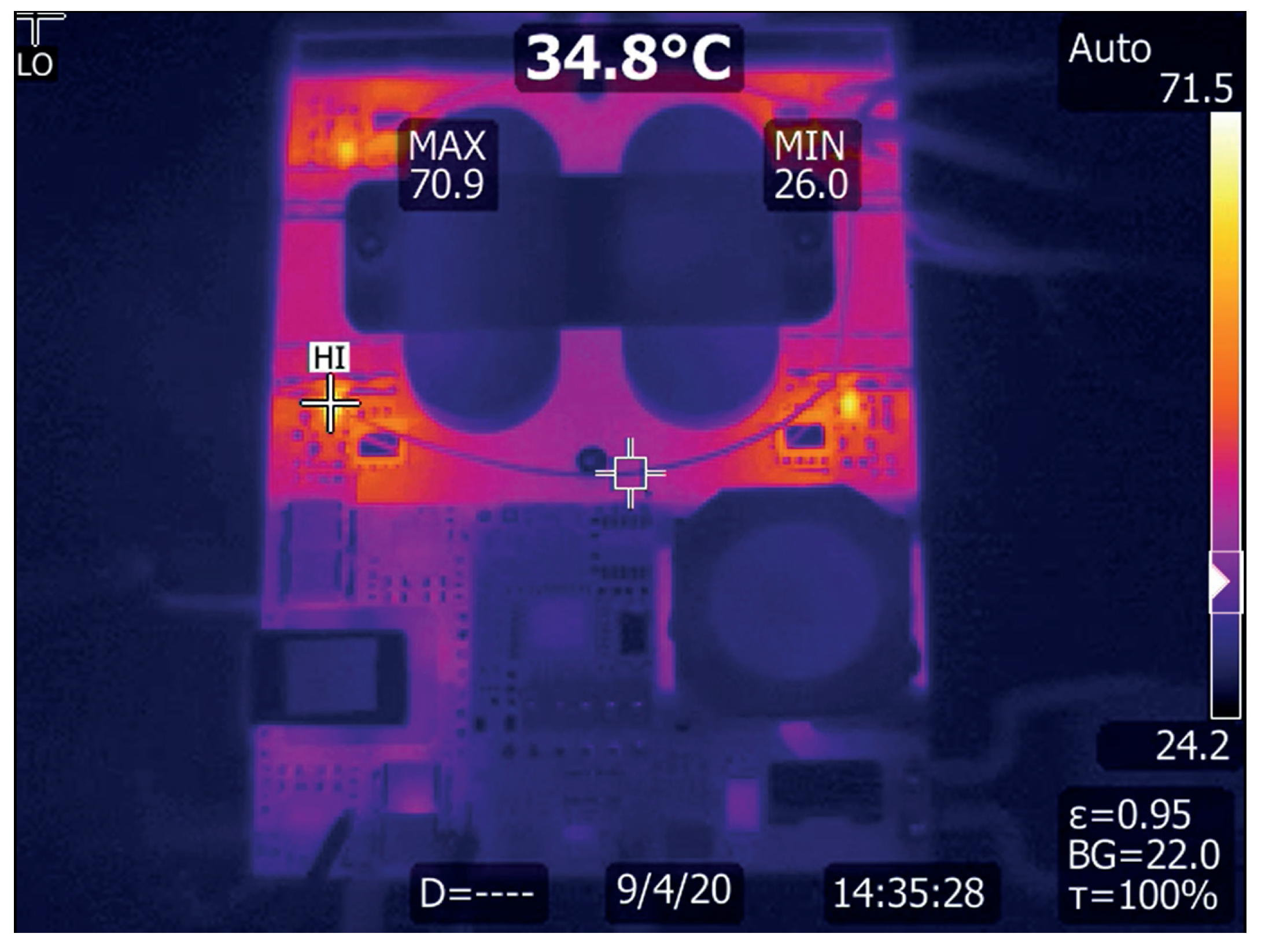
Figure 15.
Thermal image of the converter at steady-state and with forced cooling. The hottest component (71 ) is the gate driver for the synchronous rectifier switches, which each dissipate around .
Figure 15.
Thermal image of the converter at steady-state and with forced cooling. The hottest component (71 ) is the gate driver for the synchronous rectifier switches, which each dissipate around .
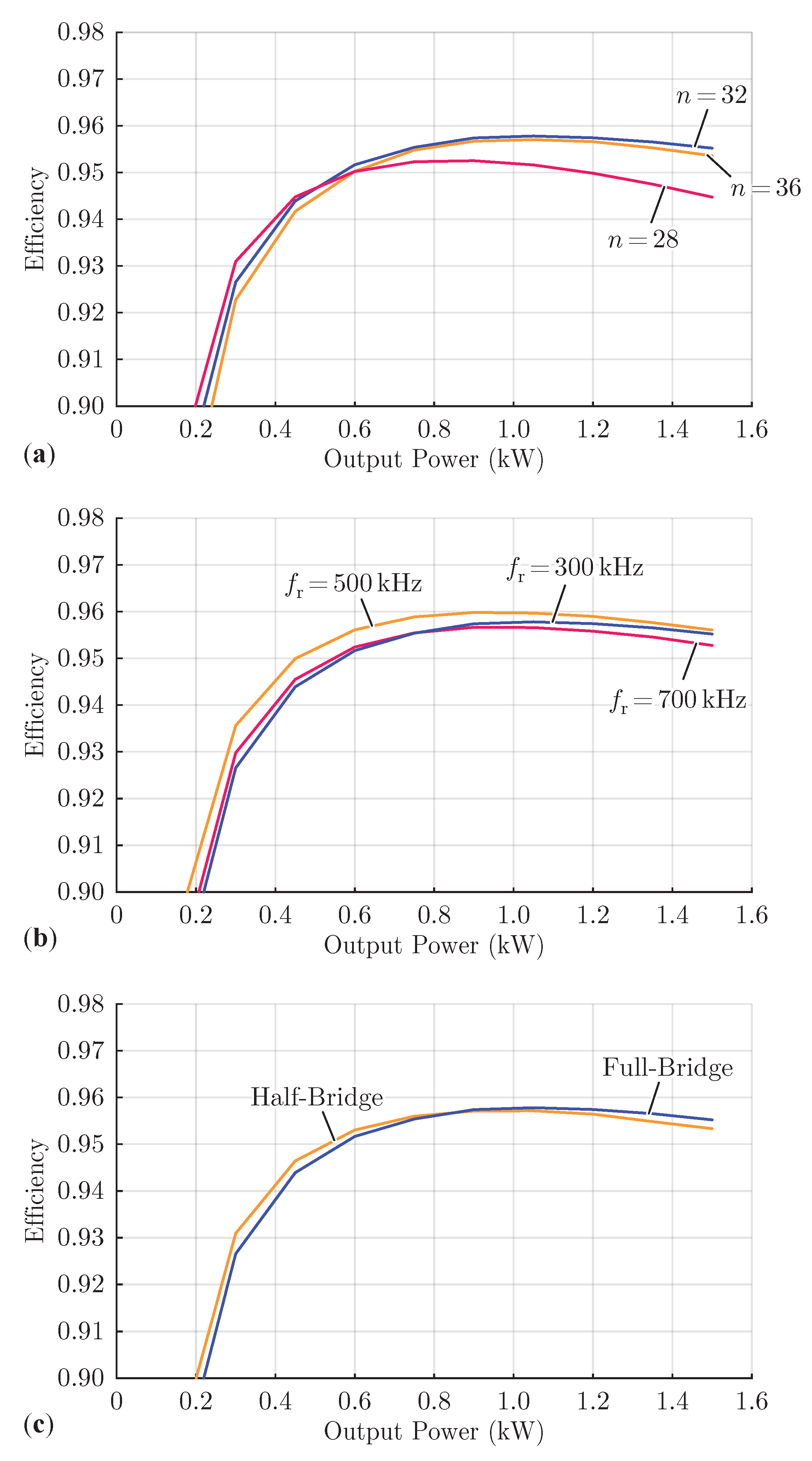
Figure 16.
Calculated efficiencies at and , highlighting optimal choices for (a) turns ratio () and (b) resonant frequency (). Due to the non-ideal synchronous rectification, body-diode conduction losses increase at higher frequencies (practical behavior not captured by the loss models), which actually makes the best choice to maximize efficiency. (c) A HV half-bridge switching-stage (that prevents DCM operation) does not improve efficiency over the full-bridge, even though n is cut by half.
Figure 17.
Transformer Pareto front optimized at 50% load by increasing limb and yoke cross-sectional areas according to case (i) of
Figure 18a, which shows that
/
of core/winding losses is optimal on
Figure 18b.
Figure 17.
Transformer Pareto front optimized at 50% load by increasing limb and yoke cross-sectional areas according to case (i) of
Figure 18a, which shows that
/
of core/winding losses is optimal on
Figure 18b.
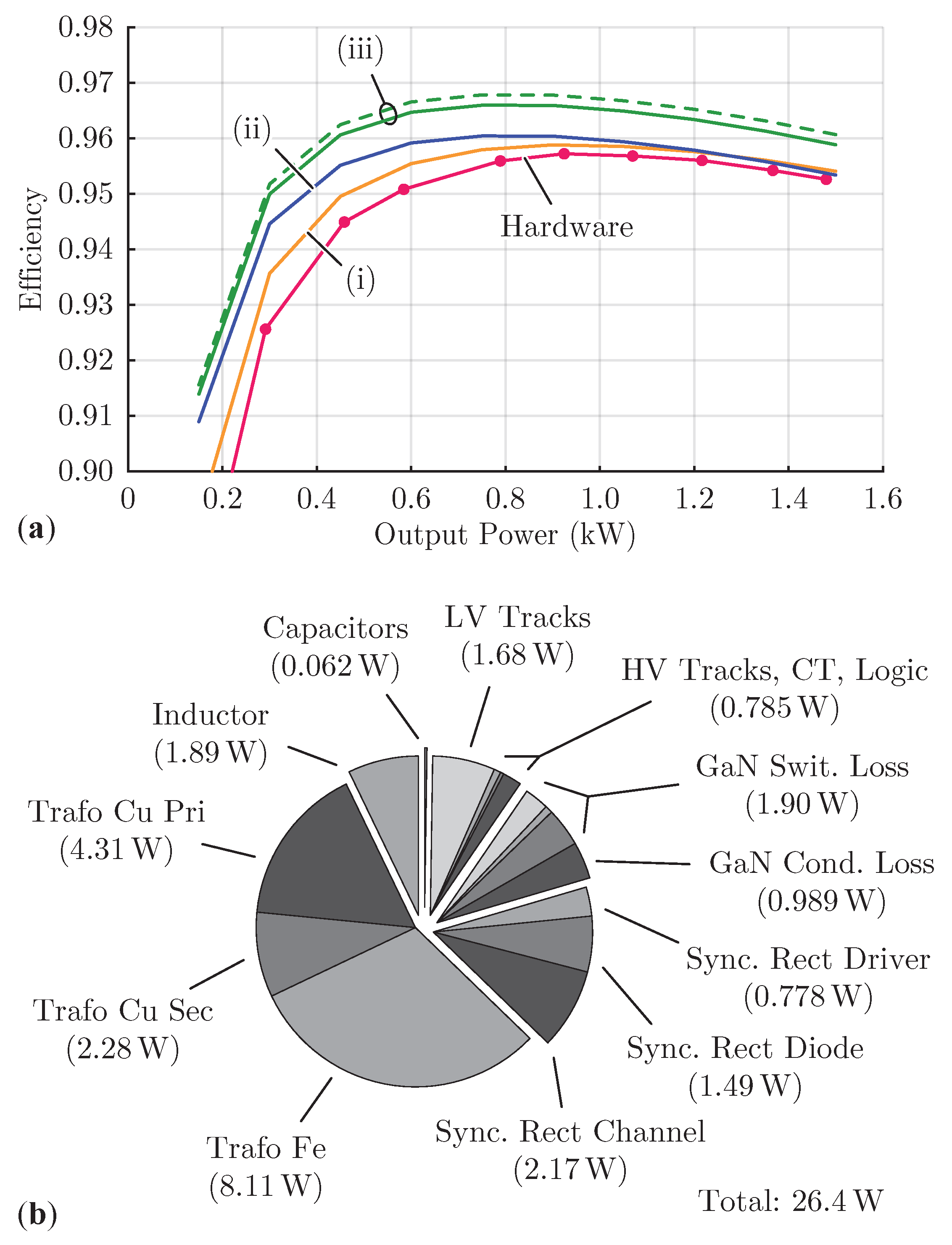
Figure 18.
(a) Calculated efficiencies (i,ii,iii) as result of a series of improvements for comparison with the prototype’s measured efficiency (“Hardware”): (i) larger limb and yoke cross-sectional areas for reduced core losses; (ii) new LV-side switch (IQE013N04LM6) with lower gate charge and triggered by a lower gate voltage using an LDO (6 instead of 12 ); and (iii) 50% lower body-diode conduction time (dashed line shows the ideal case of no body-diode conduction). (b) Loss budget of case (iii) at 50% load.
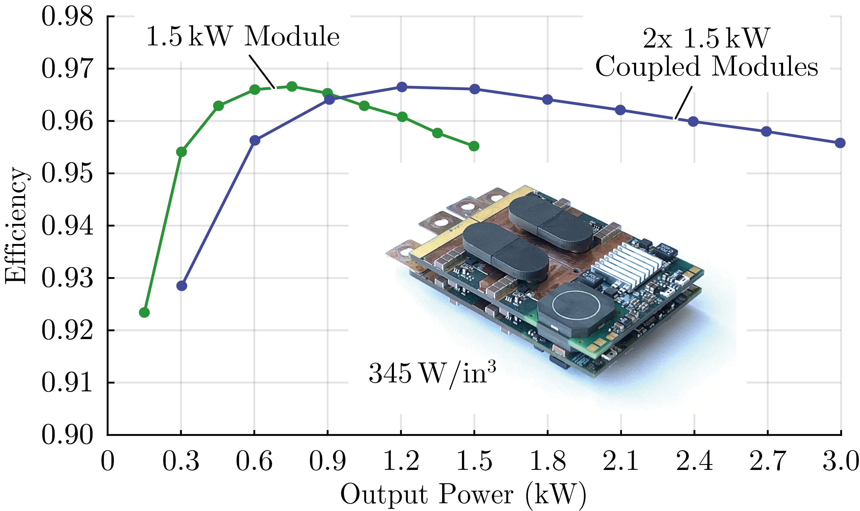
Figure 19.
Next-generation DC/DC module (key values and implementations given in
Table 7), measuring
×
×
(308
), shown with two modules combined in an input-parallel output-parallel (IPOP) configuration to reach 3
output power at 250
of output current and measuring
×
×
(345
). The snake-core transformer enables ideal current sharing between the phases and modules with reduced core losses from the single flux path and shared transformer core between the two modules.
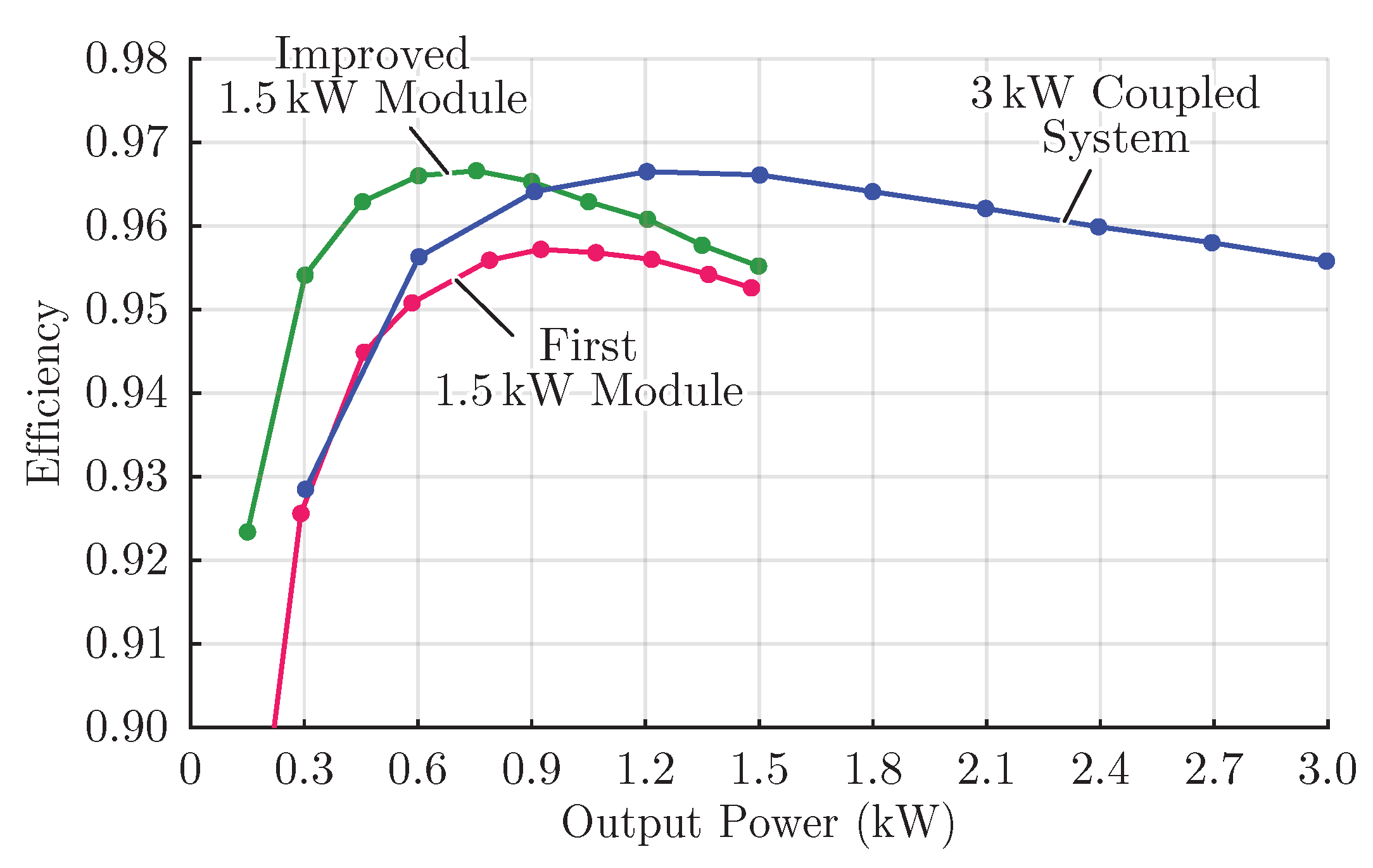
Figure 20.
DC/DC electrically-measured efficiencies from input () to output () at different load conditions, including all loss components. The improved DC/DC module achieves higher efficiency than the original module at all load conditions, and the paralleled 3 converter achieves higher efficiency from reduced core losses at power levels below .
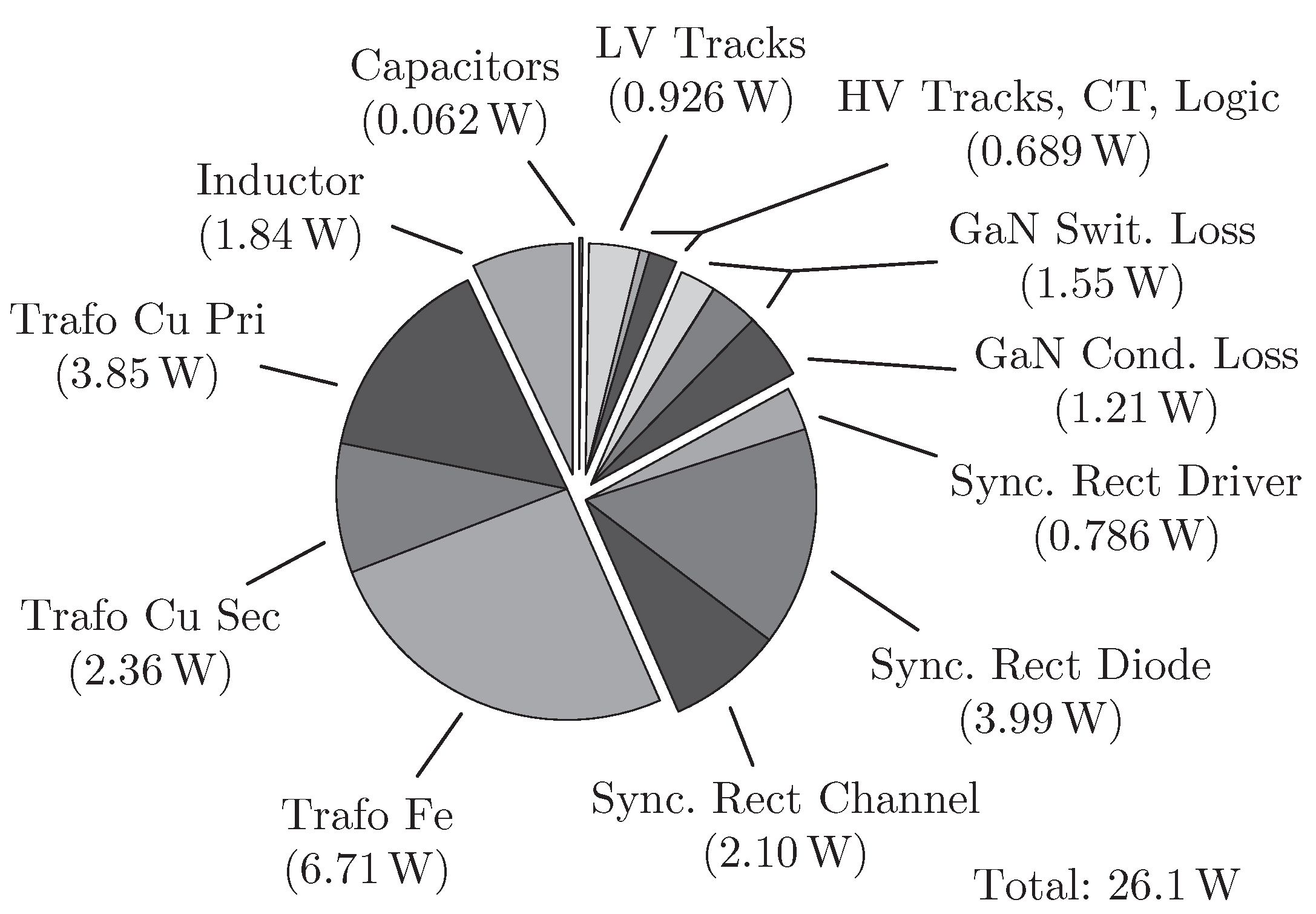
Figure 21.
Experimental loss budget at 50% load of the ”Improved
Module” of
Figure 20 (”Module 1” in
Figure 19), with
and
, confirming the expected performance improvements calculated in
Figure 18b.
Figure 21.
Experimental loss budget at 50% load of the ”Improved
Module” of
Figure 20 (”Module 1” in
Figure 19), with
and
, confirming the expected performance improvements calculated in
Figure 18b.
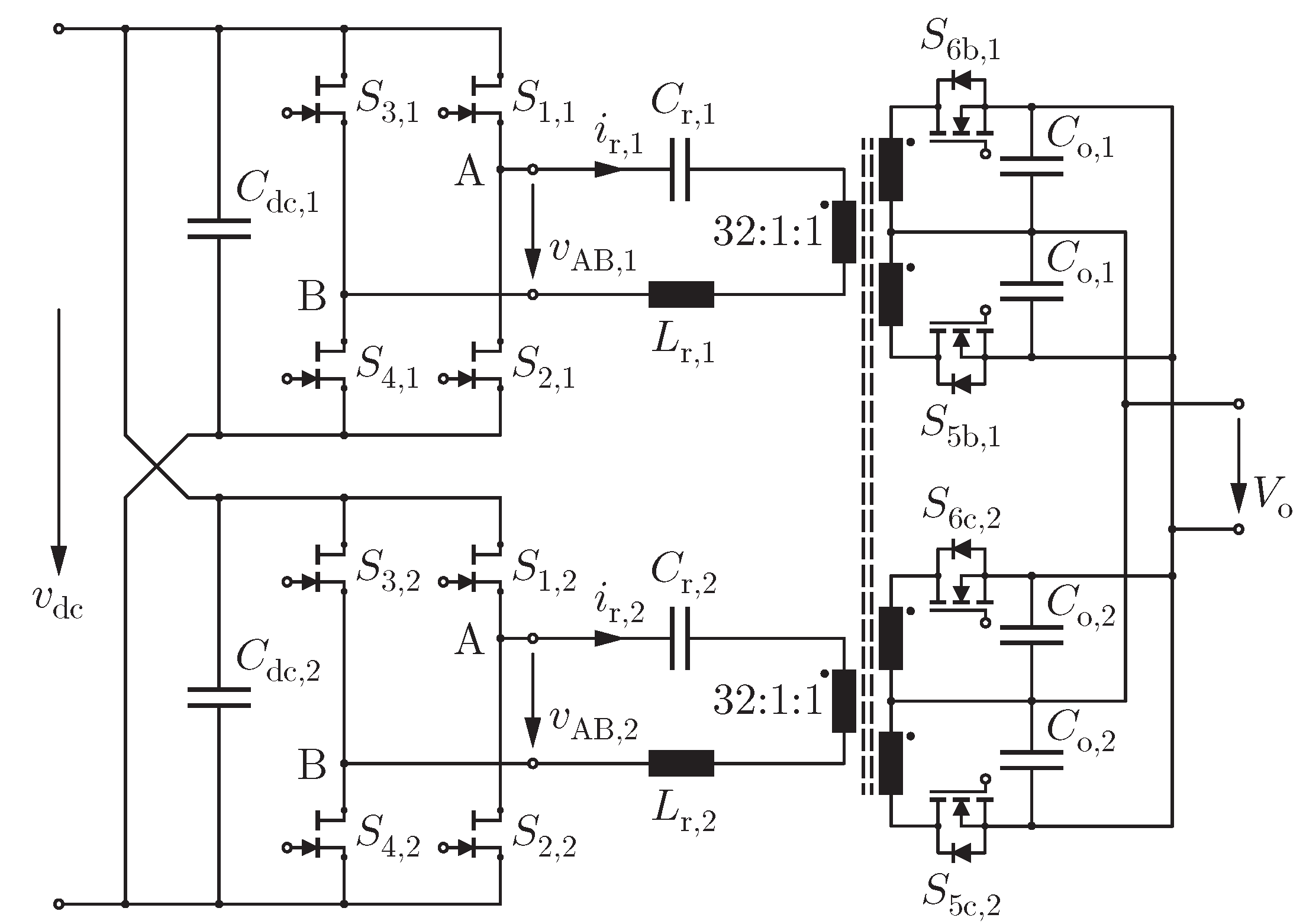
Figure 22.
Simplified power circuit of the proposed input-parallel output-parallel (IPOP) combined DC/DC converter, with the snake-core transformer shared for a single flux path between the two modules that results in ideal current sharing, lower core losses, and improved power density. The converter utilizes GaN devices for the primary-side full-bridge and the updated IQE013N04LM6 power MOSFETs operating as synchronous rectifiers on the secondary-side.
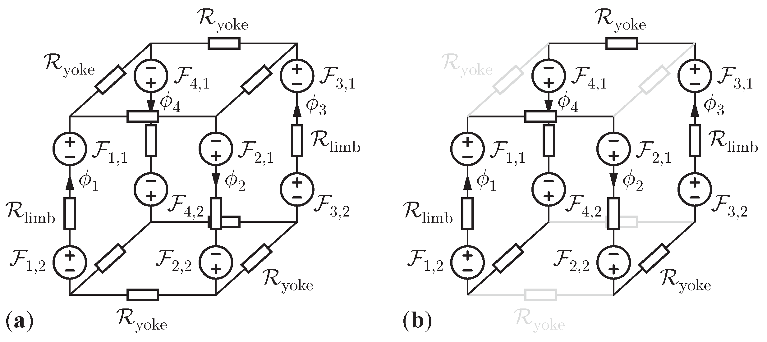
Figure 23.
Magnetic circuits for (a) a conventional matrix transformer and (b) the proposed snake-core transformer, with the magnetomotive forces of the windings () and core reluctances () highlighted, assuming the permeability of the core is sufficiently high to ignore reluctance paths through the air. The snake-core transformer has only a single path for the flux, guaranteeing identical flux through every winding and resulting in ideal current sharing. The conventional matrix transformer has multiple flux paths, and small turns or reluctance mismatches therefore result in poor current sharing and, potentially, operation instability.
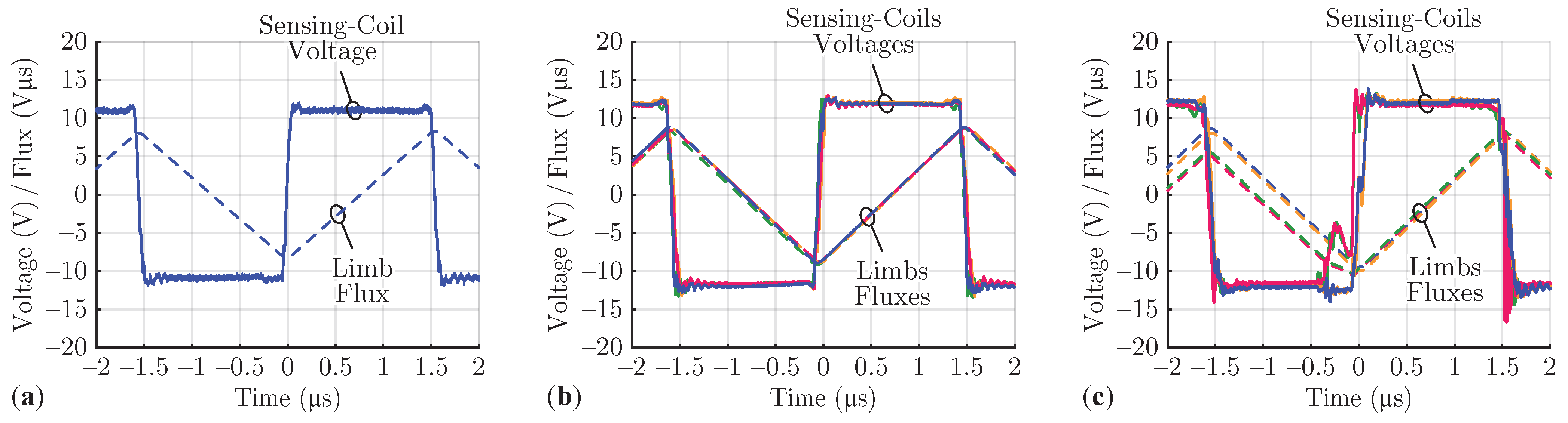
Figure 24.
Measured induced voltages and limb fluxes (measured by sensing coils wound around the core limbs) for (a) the proposed snake-core transformer, and for the conventional matrix transformer with (b) balanced and (c) unbalanced reluctances, through the addition of an larger air gap in one leg. Output power is 40% load for all test conditions.
Table 1.
DC/DC module design specifications.
Table 1.
DC/DC module design specifications.
| Full-load output power () | |
| Output voltage () | 12 |
| Full-load output current () | 125 |
| Power density | 300 (
) |
| Footprint (l × w) | 10 × 7 |
| Height (h) | |
| Input voltage range () | 300 –430 |
| PCB-integrated | Yes |
| Full ZVS | Yes |
| Parallel-able | Yes |
Table 2.
Survey of published converters near the design specifications of the DC/DC module considered in this paper. Efficiency is given at nominal load () and 50% of nominal load ().
Table 2.
Survey of published converters near the design specifications of the DC/DC module considered in this paper. Efficiency is given at nominal load () and 50% of nominal load ().
| Ref. | Topology | Full
ZVS? | | / | Power Density | Eff.
() | Eff.
() | PCB-
int.? |
|---|
| [14,16] | LLC | Yes | 380 | 12 /83 | 700 | %
| %
| Yes |
| [17] | LLC | Yes | 380 | 12 /67 | 900 | %
| %
| Yes |
| [15] | LLC | Yes | 200 –420 | 12 /83 | — | %
| %
| No |
| [15] | PSFB | No | 200 –420 | 12 /83 | — | %
| %
| No |
| [21] | PSFB | Yes | 270 | 22 /68 | — | %
| %
| No |
| [22] | PSFB | Yes | 230 –430 | 14 /150 | 170 (target) | %
| %
| Yes |
| [19] | PSFB | Yes | 330 –420 | 12 /83 | 300 (package) | %
| %
| Yes |
| [18] | Double-clamp | Yes | 160 –420 | /130 | 900 (package) | %
| %
| Yes |
| [8] | Half-bridge | No | 150 –400 | 12 /167 | — | %
| %
| No |
| [9] | DAB | No | 240 –450 | 12 /182 | 25 | %
| %
| No |
| [10] | DSAB | No | 350 –410 | 12 /25 | ≈ | %
| %
| Yes |
| [12] | LLC | Yes | 280 –380 | 48 /2 | ≈ | %
| %
| Yes |
| [13] | Morphing LLC | Yes | 100 –400 | 48 /17 | — | %
| — | No |
| [20] | PSFB | Yes | 300 –400 | 50 /24 | — | %
| %
| No |
| Target | | Yes | 300 –430 | 12 /125 | 300 | | | Yes |
Table 3.
Comparison between predicted and measured winding losses for the PCB-integrated transformer. All parameters at .
Table 3.
Comparison between predicted and measured winding losses for the PCB-integrated transformer. All parameters at .
| | Freq.
(kHz) |
(kHz) |
(m) | Error
(%) |
|---|
| DC | 244.2 | 256.5 | −4.8 |
| DC | 0.2085 | 0.2166 | −3.7 |
| 300 | 755.2 | 758.0 | −0.4 |
| 500 | 892.5 | 906.6 | −1.6 |
| 700 | 1030 | 1027 | 0.3 |
| DC | 0.03622 | 0.03554 | 1.9 |
Table 4.
Design characteristics of the optimized transformer and inductor.
Table 4.
Design characteristics of the optimized transformer and inductor.
| | Transformer | Inductor |
|---|
| Winding width | | |
| Limb area () | 48 | 36 |
| Yoke area * () | 71 | 149 |
| Air-gap length () | | |
Table 5.
Comparison between predicted and calorimetrically-measured core losses for the PCB-integrated transformer.
Table 5.
Comparison between predicted and calorimetrically-measured core losses for the PCB-integrated transformer.
| | #1 | #2 | #3 | #4 |
|---|
| () | 0.156 | 0.166 | 0.176 | 0.149 |
| () | 0.113 | 0.121 | 0.129 | 0.148 |
| () | 85.9 | 92.4 | 103 | 105 |
| () | 1.01 | 1.64 | 2.77 | 1.73 |
| () | 3.99 | 5.67 | 8.99 | 17.1 |
| () | 0.0033 | 0.0038 | 0.0043 | 0.0057 |
| () | 0.0344 | 0.0391 | 0.0442 | 0.0581 |
| () | 5.04 | 7.45 | 11.8 | 18.9 |
| () | 4.61 | 6.91 | 10.7 | 17.5 |
| Error (%) | 9.3 | 7.8 | 10.3 | 8.0 |
Table 6.
Key design values and implementation for components in the
hardware demonstrator of
Figure 11.
Table 6.
Key design values and implementation for components in the
hardware demonstrator of
Figure 11.
| Parameter | Design Value | Implementation |
|---|
| – | 600 , 70 GaN HEMT IGLD60R070D1 |
| gate drivers | – | UCC21225A |
| – | 40 , Si MOSFET TPW48004PL |
| gate drivers | – | NCP4306 and UCC27511A, |
| 24 | PCB-integrated, fringing-field concept [25] |
| 1 | C5750X7T2W105K250KA |
| 640 | 20 C4532X7R1C336M250KC |
| 11 | CGA4F4C0G2W222J085AA |
Table 7.
Key design values and implementation for components in the
Improved hardware demonstrator of
Figure 19.
Table 7.
Key design values and implementation for components in the
Improved hardware demonstrator of
Figure 19.
| Parameter | Design Value | Implementation |
|---|
| – | 600 , 70 GaN HEMT IGLD60R070D1 |
| gate drivers | – | UCC21225A |
| – | 40 , Si MOSFET IQE013N04LM6 |
| gate drivers | – | SRK2001A and 1EDN7511B, |
| 24 | PCB-integrated, fringing-field concept [25] |
| 1 | C5750X7T2W105K250KA |
| 640 | 20 C4532X7R1C336M250KC |
| 11 | C3216C0G2J222J115AA |


 ,
, 


