Abstract
This paper presents the design and postlayout simulation results of a capacitor-less low dropout (LDO) regulator fully integrated in a low-cost standard 180 nm Complementary Metal-Oxide-Semiconductor (CMOS) technology which regulates the output voltage at 1.2 V from a 3.3 to 1.3 V battery over a −40 to 120 °C temperature range. To meet with the constraints of system-on-chip (SoC) battery-operated devices, ultralow power (Iq = 8.6 µA) and minimum area consumption (0.109 mm2) are maintained, including a reference voltage Vref = 0.4 V. It uses a high-gain dynamically biased folded-based error amplifier topology optimized for low-voltage operation that achieves an enhanced regulation-fast transient performance trade-off.
1. Introduction
The increasing appearance of long-life autonomous portable and wearable equipment [1,2,3,4,5,6,7,8] demanding miniaturized systems with decreasing power consumption has brought to the forefront the design of efficient power management units (PMU), where low dropout (LDO) regulators play a key role [9,10,11,12,13]. As shown in Figure 1, in battery-operated systems, the LDO generates, from the battery voltage VBAT, a stable, low-noise and accurate supply voltage Vout under substantial changes of the battery voltage and the load current demanded to bias a specific system module, typically making use of multiple LDOs so as to optimize each module power consumption and, therefore, the global power efficiency.
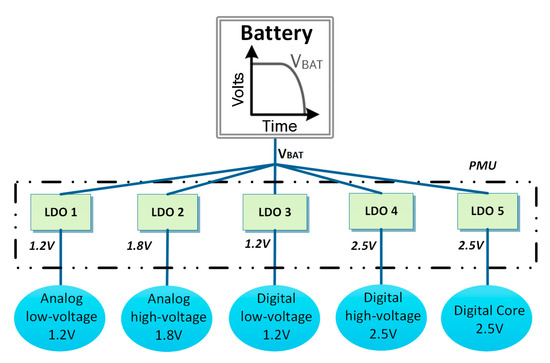
Figure 1.
Power management system using multiple LDOs (low dropout).
Conventional LDOs rely on external µF capacitors located at the output node to guarantee stability and at the same time to minimize the variations on Vout under transient operation [14,15,16]. Nonetheless, the reduction in power and size of the systems is leading toward complete system-on-chip (SoC) devices, where all the components need to be fully integrated. A key condition in the implementation of low-cost system-on-chip solutions is compatibility with complementary metal–oxide–semiconductor (CMOS) technology. This, in turn, has been associated with low-voltage compliance, since as CMOS technology downscales, the supply voltage also downscales, very nearly approaching the threshold voltage of MOS transistors, such that the new strategies must be followed when designing such low-voltage circuits.
Therefore, the design of CMOS capacitor-less low-dropout regulators has become a promising research topic, requiring low-voltage architectures with alternative on-chip compensation techniques that maintain the stability of the system over all the operating range while preserving the regulating performance. Moreover, a key parameter in portable devices is power consumption, since it determines the battery life. This implies the use of low quiescent currents Iq. However, reducing Iq degrades the dynamic performance: the maximum output current is limited, thus limiting parameters such as slew-rate and settling time. This makes necessary the introduction of transient enhancement circuit techniques to balance the dynamic performance with a minimum effect on power efficiency and circuit complexity.
There is extensive research on low dropout regulators for portable applications by taking advantage of the miniaturization of CMOS technology [17,18,19,20,21,22,23,24,25,26]. However, some of them report load capacitor values that do not comply with the size constraint of portable SoC devices ([17] and [18] report external load capacitors of 1 µF and 3 nF, respectively). Among those that are fully integrated, power consumption is jeopardized by quiescent currents too high to be used in short-lived battery-operated devices ([19] reports 495 µA, [20] 188 µA, [21] 76 µA and [22] 265 µA). Other proposals enhance the transient response by using adaptive biasing but jeopardizing the circuit complexity and power consumption ([23] increases the Iq from 4.45 µA for ILoad = 100 µA up to 130 µA for ILoad = 100 mA; and the Iq from [24] goes from 42.1 µA for ILoad < 1 mA up to 108 µA ILoad > 1 mA). Moreover, some LDOs require a minimum load current for stability, and therefore, the total current consumption is actually Iq + ILoad,min, further reducing the battery life ([25] reports a minimum load current of 250 µA, [21,23,26] 100 µA, [22] 10 µA and [20] 1 mA). Accordingly, there exists an overall power-area-transient behavior trade-off that makes the design of a fully integrated stable LDO a significant challenge, with high regulation performance and good dynamic performance, preserving ultralow power consumption and a compact topology.
In this proposal, an all-MOS capacitor-less low dropout (LDO) regulator is presented with improved performance aimed at this demanding scenario of portable on-chip devices. Thus, design guidelines are used to minimize both the power and area consumption, while maintaining an adequate regulating performance with a low-voltage topology for our requirements: a 1.2 V output voltage, Vout, compatible with battery supply voltage values VBAT = 3.3 − 1.3 V, for a maximum ILoad = 50 mA over a CLoad,max = 50 pF. In this attempt, we have followed the compensation and dynamic-enhancement strategies successfully adopted in [27] but adapted to provide the required low-voltage compatibility, further optimizing the transient response by introducing a multiple dynamic feedback strategy. Moreover, a fully integrated temperature and voltage-supply-independent voltage reference are also proposed to further advance into a truly integrated device.
Some preliminary results were reported in [28]. In this paper, the optimized design and complete postlayout characterization of the LDO are presented. The organization of this paper is as follows: in Section 2, the design of the low dropout (LDO) regulator is presented; the characterization and comparison with other LDO regulators is reported in Section 3. Finally, in Section 4, conclusions are drawn.
2. Proposed Topology
In this section, the operating principle of a LDO regulator is introduced together with the schematic design of the proposed 1.2 V LDO regulator.
Figure 2a illustrates the basic scheme of a linear regulator, which provides a regulated voltage Vout from an unregulated input voltage Vin, which is the battery voltage VBAT for the power management unit of a battery-operated portable device [29]. A sampling circuit is responsible for sensing the variations over Vout because of variations in the power supply and/or in the load current. An error amplifier (EA) compares the difference between this signal and a reference voltage, Vref, and drives the control element, which makes the necessary modifications to set the desired voltage at the output.
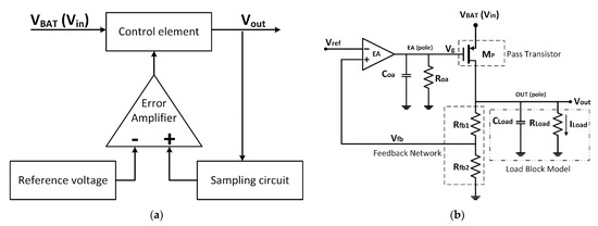
Figure 2.
(a) Conceptual scheme of a linear regulator and (b) schematic view of a complementary metal–oxide–semiconductor (CMOS) LDO regulator.
Figure 2b presents the typical scheme of a CMOS LDO regulator, which uses a PMOS transistor as the control element to minimize the dropout voltage Vdo = VBAT − Vout and a resistive network Rfb1 − Rfb2 as a sampling circuit. This negative feedback resistive network samples the output voltage Vout through a feedback voltage Vfb, which is compared against the reference voltage, Vref. The variation is amplified and applied to the PMOS transistors gate, Vg, acting as the control element to keep the desired output voltage constant regardless of the changes in the supply voltage, Vin, or the current required by the load, modelled through RLoad and CLoad.
Assuming an ideal amplifier, the output voltage is then given by
The main design parameters for low dropout regulators include stability, line regulation (LNR), load regulation (LDR), line transient regulation, load transient regulation and power supply rejection (PSR). To achieve a high level of precision in the regulation, the use of high gain error amplifiers is required, as shown by Equations (2) and (3) [30]. The load regulation is approximated to:
and line regulation
where gmP is the pass transistors transconductance, AV the open-loop gain of the EA, and α is the feedback factor set by Rfb2/(Rfb1+Rfb2). Therefore, since both LNR and LDR are inversely dependent to the error amplifier DC gain, the higher the AV, the better the regulation.
The simplest amplifier topology is a differential pair. To increase its gain without power penalty, a cascode configuration is used, obtaining the so-called telescopic amplifier. This structure, however, implies the use of several stacked transistors, a technique unfit for low-voltage solutions. To take advantage of the cascode technique to increase the amplifier gain with a topology suitable for low-voltage operations with minimum power penalty, the folded-cascode amplifier is used. Thus, a folded-cascode structure is considered. By using this simple one-stage topology, we are able to lower both the requirements for power and area consumption, simplifying altogether the LDO compensation, which corresponds to a two-pole system (Figure 2b), one at the pass transistor gate, and given by:
where Roa and Coa characterize the output impedance of the error amplifier and CgsP the gate-source capacitance of the PMOS pass transistor.
The second pole is located at the LDO output and is given by:
To achieve a stable SoC LDO regulator over all the ILoad operating conditions, the dominant pole of the system must be placed, through internal compensation techniques, at the output of the error amplifier, fEA, while the pole located at the output of the LDO regulator must satisfy fOUT ≫ fEA.
2.1. Core Structure
The core structure, as shown in Figure 2b consists of a reference voltage Vref = 0.4 V, a PMOS pass transistor MP, a resistive feedback network and an EA, and its schematic is shown in Figure 3. To guarantee the operation of the PMOS pass transistor in saturation for maximum ILoad = 50 mA with a Vdo = 300 mV, its size is set to 9 mm/340 nm. In order to minimize the parasitic gate pass transistor capacitance CgsP—which is ~11 pF with no load and up to 17 pF at the maximum load- the transistor length used is the minimum allowed by the technology.
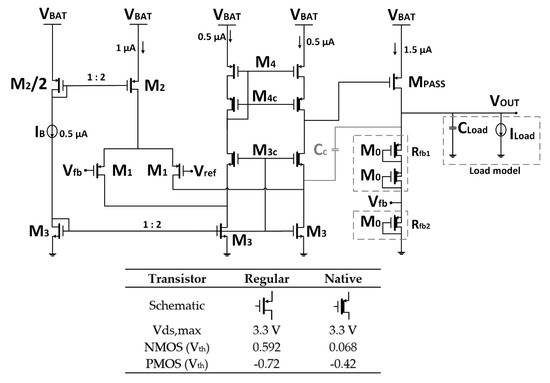
Figure 3.
Core structure of the proposed CMOS LDO regulator for a 1.2 V output.
The static current through the pass transistor is set to 1.5 µA at no load current condition to keep a low power consumption. With a Vout = 1.2 V and a reference voltage Vref = 0.4 V, the resistive feedback network results in Rfb1 + Rfb2 = 800 kΩ with Rfb1 = 2Rfb2. These resistances have been carried out through three identical low-voltage PMOS transistors in a P-substrate N-well technology (M0, size 1 µm/1 µm, with VBS = 0) in diode configuration to further optimize the area, resulting in an area reduction of ~250 times, compared to its implementation with a highly resistive polysilicon layer of the technology (Rsquare = 1039 Ω/square).
A folded-cascode PMOS-input differential amplifier implements the error amplifier. It is a single-stage high-gain structure specifically designed for low-voltage applications. Consequently, good line regulation (LNR) and load regulation (LDR)—Equations (2) and (3)—are achieved while the power consumption is maintained bounded and compensation is simplified [31]. Low-voltage transistors (native to the technology) are used for both the cascode transistors, using a self-biased scheme (gates of M4 and M4C are connected, and the same happens with M3 and M3C); with this method, no additional bias branches are required (Figure 3). All other transistors in the circuit are 3.3 V regular. Figure 3 also details the schematic view of the two transistors (native and regular) and their main parameters.
Transistor sizes (µm/µm) of the error amplifier are M1 = 60/0.34, M2 = 12/4, M3 − M3c = 8/2 and M4 − M4c = 6/2. With a total Iq of 3.5 µA (including the 0.5 µA bias current), it presents a gain > 85 dB, phase margin PM = 89° and gain-bandwidth product GBW > 105 kHz over the battery voltage range (1.3 V − 3.3 V) and the parasitic CPASS range of the pass transistors gate (11 pF@ILoad = 0 mA/17 pF@ILoad = 50 mA).
As shown in Figure 4, fOUT moves toward higher frequencies for higher load currents rendering the system stable. However, as the load current reduces, fOUT approaches fEA, reducing the phase margin down to 32°, i.e., under the (45°–60°) limit that guarantees stability [32]. Thus, to separate the poles and keep the system stable, a single MIM capacitor CC = 6.1 pF (78 µm/78 µm size) is used as a cascode compensation technique (in grey in Figure 3), attaining a PM above 60.3° over all the working conditions (Figure 4).
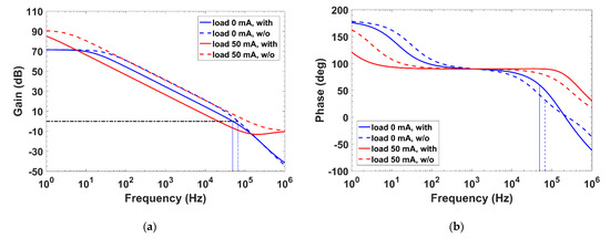
Figure 4.
(a) Gain and (b) phase margin with (straight line) and w/o (dotted line) compensation for maximum ILoad (50 mA, red) and minimum ILoad (0 mA, blue).
2.2. Transient Response
The combination of a low quiescent current, Iq, coupled with the limited slew-rate at the error amplifier output node due to the high pass transistor gate capacitance, as well as the small load capacitor compared to the conventional externally compensated µF load capacitor LDOs results in large time responses and voltage peaks, as it can be seen in the characterization of the transient load regulation without any circuit to enhance the dynamic behavior, shown in Figure 5. It provides settling times of roughly 35.4 and 14.2 µs for the overshoot (OS) and the undershoot (US) performance, respectively, with voltage peaks of approximately 1.64 V (OS) and 759 mV (US). These values clearly demonstrate the need of a transient control circuit capable of stabilizing the output voltage faster and with smaller voltage peaks, while at the same time keeping the constraints of reduced area and power consumption.
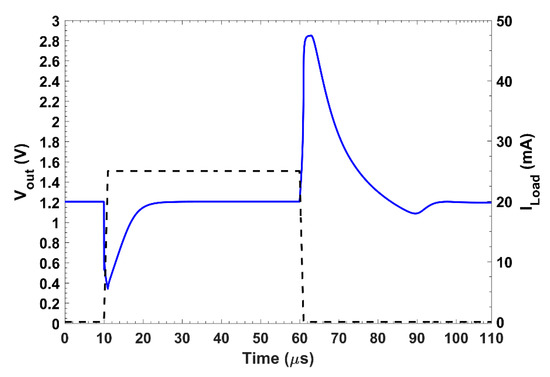
Figure 5.
Load transient behavior, from 0 to 50 mA, w/o transient enhancement with VBAT = 3.3 V.
This is performed through a simple but effective dynamic transient control (TC) circuit, only active during the transients, so that both the additional circuit complexity and power consumption remain bounded as shown in grey (transient control circuit, TC) in Figure 6. The overshoot (OS) transient detection circuit consists of a NMOS quasifloating gate (QFG) transistor MQFG,N, with the voltage gate set to a DC bias VBN connected using a large resistance realized by two series reversed-biased PMOS transistors in diode configuration and linked to the output node through a capacitor CQFG = 1 pF. In a steady state, the gate to source voltage is VGS = VBN = 0.4 V < VTH,N = 0.59 V; therefore, MQFG,N stays in the cut-off region with a weak leakage current consumption. Meanwhile, when ILoad suddenly decreases, the overshoot at Vout couples through CQFG triggering on the transistor and generating a current. This current is directly added to the error amplifiers lower Ibias branch at node C, assisting the gate capacitance CPASS charge. In addition, MQFG,N is duplicated to MQFG,N′ dynamically sinking supplementary current at the output node of the LDO regulator, aiding to discharge the path made by (Rfb1 + Rfb2) and CLoad. When Vout is regulated back to its nominal value, MQFG,N returns to the off region.
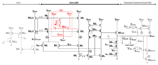
Figure 6.
Core structure of the proposed low dropout regulator with transient control circuits.
For the undershoot (US) transient detection circuit, a similar circuit based on two identical QFG PMOS transistors MQFG,P is used. Again, with a DC bias voltage VBP connected to the voltage gate through a RLarge resistive element and to Vout through a CQFG capacitor of 1 pF. In a steady state, the transistor remains in the cut-off region with the voltage gate being VSG = (VBAT − VBP) = 0.55 V < |VTH,P| = 0.72 V. Afterward, when Vout suddenly decreases, the variation is conveyed to MQFG,P transistors gate, turning VSG > |VTH,P| entering the on region of the transistors. The newly generated currents are added to the error amplifiers upper Ibias branches at nodes A and B, respectively, hastening the gate capacitance CPASS discharge. When Vout is taken back to its nominal value, MQFG,P returns to the off region.
To further improve the US transient behavior, Figure 6 shows in red another QFG approach (transient enhancement circuit, TEC) that adds dynamic current sources MDB in parallel to the currents at nodes A and B. In a steady state, VG,MDB = VG,M2 and transistors are in a saturation region driving a static current of 1 μA each. When Vout decreases, the variations are coupled to their gate through capacitor CQFG, accelerating the discharge process.
Transistor sizes (µm/µm) of the transient control circuits are MQFG,P = 180/0.34, MQFG,N = 180/0.34, MQFG,N’ = 20/0.34 and MDB = 12/4, with RLarge = 0.5/5 and CQFG = 1 pF implemented as two MIM capacitors (22.2 µm/22.2 µm size each). The complete schematic structure of the core LDO regulator with the transient enhancement circuits (TC and TEC) is shown in Figure 6, while the improvement of the transient circuits is presented in Figure 7.
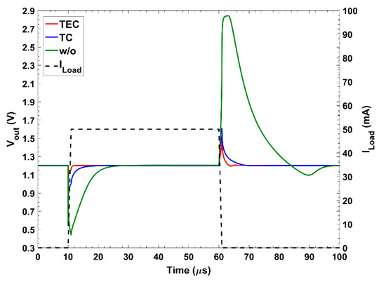
Figure 7.
Impact of the transient enhancement circuits on the load transient behavior (at VBAT 3.3 V).
2.3. Voltage Reference Circuit
Finally, to truly achieve a fully integrated LDO, the voltage reference Vref = 0.4 V is also implemented on-chip. Observe that as per Equation (1), Vout is directly dependent of the reference voltage. Therefore, any dependence on the temperature and/or the battery voltage in Vref is transferred to Vout.
This voltage reference is typically implemented as a bandgap voltage reference with a combination of complementary to absolute temperature (CTAT) and proportional to absolute temperature (PTAT) voltages or currents to provide a reliable temperature and supply independent solution [33,34,35,36,37,38]. However, the classical approaches typically provide higher values than the low-voltage 0.4 V approach herein adopted, while usually demanding high levels of power and area consumption not suitable for miniaturized portable systems.
Therefore, the 0.4 V voltage reference proposed here is based in the technique used for a 2-transistor (2T) Vref ([39], Figure 8a), which takes advantage of different transistors with different threshold voltages Vth (one regular thick oxide Vth,r and one native device Vth,n) operating in the subthreshold region. Therefore, the voltage reference performance can be modelled from the subthreshold current equation:
where β = µCOX(W/L) with μ being the mobility of the electrons, COX the oxide-capacitance and (W/L) the transistors dimensions; m is the emission coefficient; VT = KBT/q corresponds to the thermal voltage with KB Boltzmann’s constant, T the temperature and q the electron charge; Vgs is the gate-to-source voltage; Vth the threshold voltage and Vds the drain-to-source voltage.
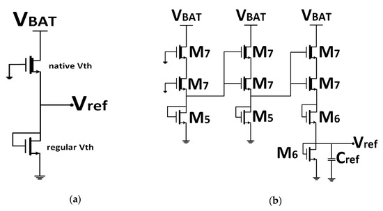
Figure 8.
Vref schematic view of: (a) 2T proposal from [39] and (b) implemented proposal.
For the topology in Figure 8a, setting the current equal through the native and the regular transistor, the reference voltage is given by [39]:
By using this 2T topology, Vref values are below the 0.4 V target reference voltage. To achieve the required voltage level, the 2T variant cascades three stages as shown in Figure 8b increasing the voltage reaching the 0.4 V, similar to the 4T Vref presented in [39] and the 6T used in [40]. In the 180 nm technology used the threshold voltages for NMOS transistors are Vth,r = 0.592 V and Vth,n = 0.068 V. Transistor sizes (μm/μm) are M5 = 0.5/0.5, M6 = 0.24/0.5, M7 = 225/0.5, such that Vref = 0.4 V with a total Iq of 20.4 nA and an output capacitor Cref = 0.5 pF is added to the output to enhance its transient performance.
3. Characterization
The proposed LDO design has been implemented in the 180 nm CMOS technology from UMC. The layout view is shown in Figure 9 with a total area consumption of 382 µm × 285 µm. The reported postlayout simulation results have been executed using Spectre with a BSIM3v3 level 53 transistor model. A 0.5 μA bias current is inserted to the circuit through a 1:2 current mirror, displaying a total Iq in steady state of 5.5 μA if the TC transient circuit is used and of 8.6 μA if the TEC transient circuit is added—including the generation of the bias voltages VBN and VBP-. It presents a temperature-independent voltage supply-independent Vout = 1.2 V, for a battery-supplied Vin ranging from 3.3 V down to ~1.3 V, with a Vdo ~ 100 mV and a maximum load of 50 mA and 50 pF.
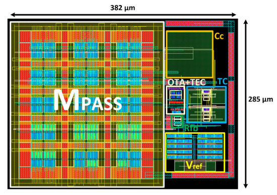
Figure 9.
Layout view of the proposed low-dropout regulator.
First, the proposed Vref is characterized against voltage and temperature variations to validate its design. Then, the static (characterized by the load regulation (LDR), the line regulation (LNR) and the quiescent current, Iq) and dynamic (characterized by the transient load and line regulations) behavior are characterized.
3.1. Voltage Reference
Figure 10a shows the temperature and Figure 10b the battery voltage, VBAT, dependence of the reference voltage, Vref, which remains almost constant at 400 mV. For a temperature variation from −40 to 120 °C the maximum Vref variation is 87.5 ppm/°C (at VBAT = 2.5 V), and for a power supply variation from 1.3 to 3.3 V, the Vref variation is 0.0155%/V (at 27 °C).
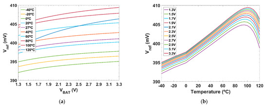
Figure 10.
Reference voltage, Vref, dependence with: (a) temperature and (b) battery voltage.
3.2. Static Behavior
Figure 11 shows the static VBAT − Vout characteristic. Figure 11a presents the results for a voltage sweep from 3.3 V down to 1.0 V, at room temperature, Troom, for different ILoad from 0 to 50 mA. The LDO regulator provides a constant Vout of 1.2 V for VBAT > 1.31 V (dropout voltage, Vdo of 110 mV) with an error < 1 % for all range of load currents. Figure 11b present the same characteristic against temperature (from −40 to 120 °C) for the designed Vref with maximum load current, showing a maximum variation of 26.8 mV (168 ppm/°C) in Figure 11b.
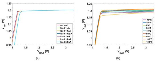
Figure 11.
Vin − Vout characteristic, with: (a) different current loads, ILoad, and (b) different temperatures (at maximum load current, ILoad).
The consumed current, Iq, by the system over the battery voltage is shown in Figure 12. Figure 12a shows the variation with both the ideal reference voltage and the designed one, showing no significant difference (around ±20 nA difference). With the proposed reference voltage, the average current consumption is 8.59 µA ± 40 nA. Figure 12b displays the quiescent current for different temperatures, showing a current increase over temperature, with a maximum deviation of ~70 nA/°C.
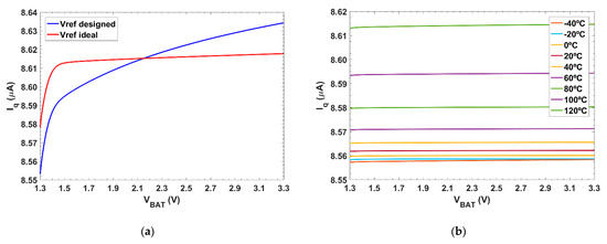
Figure 12.
Quiescent current, Iq, at: (a) room temperature, Troom; and (b) different temperatures.
Figure 13 presents the line regulation (LNR) performance for different loads (Figure 13a) and temperatures (Figure 13b). The worst-case LNR at room temperature is for ILoad = 0 mA (LNR = 4.13 mV/V). Over temperature, it shows a maximum deviation of ~156 (µV/V)/°C.
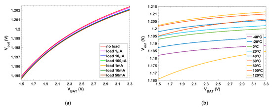
Figure 13.
Line regulation for different: (a) load currents; and (b) temperatures (under maximum load current condition).
Figure 14 presents the load regulation (LDR) performance for different VBAT (Figure 14a) and temperatures (Figure 14b). The worst-case line regulation at room temperature, is for VBAT = 3.3 V (LDR = 5.56 μV/mA). Over temperature, it shows a maximum deviation of ~4.25 (µV/mA)/°C. The load regulation is almost equal for each VBAT value, being the main affected parameter in the line regulation.
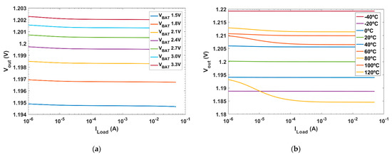
Figure 14.
Load regulation for different: (a) battery voltages and (b) temperatures (with VBAT = 2.5 V).
3.3. Dynamic Behavior
Figure 15 presents the performance for a full load transition (0 mA—50 mA—0 mA with 1 µs rise/fall times) for VBAT = 3.3 V, with and without the TC and TEC transient circuits. Figure 15a presents the undershoot (US) performance and Figure 15b the overshoot (OS) performance.
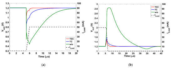
Figure 15.
Load transient behavior: with and w/o the TC and TEC transient circuits for VBAT 3.3 V: (a) undershoot and (b) overshoot.
Figure 15a shows that the suggested low-dropout regulator achieves stability for undershoot (US) variations with a 1% error for a maximum variation of 499 mV within 5.9 μs (TC); this means an enhancement of 8.3 µs and 260 mV. With the TEC circuit, shown in grey in Figure 6, the discharge process can be enhanced reducing the maximum variation down to 340 mV within 1.3 μs.
Figure 15b shows this behavior for overshoot (OS) variations; the stability is achieved with a 1% error for a maximum variation of 406 mV and within 7.5 μs (TC); and this means an enhancement of 27.9 µs and 1.23 V. With the TEC circuit, the process is enhanced reducing the maximum variation down to 326 mV within 3.0 μs.
Figure 16 presents the performance over a full line transition (1.5 V—3.3 V—1.5 V with 1 µs rise/fall times) for ILoad = 50 mA, with the TC and TEC transient circuits and without them. Figure 16a presents the undershoot (US) performance and Figure 16b the overshoot (OS) performance.
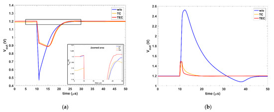
Figure 16.
Line transient behavior: with and w/o the TC and TEC transient circuits for ILoad 50 mA: (a) undershoot and (b) overshoot.
Figure 16a shows that for undershoot (US) variations stability is achieved with a 1% error for a maximum variation of 307 mV within 13.6 μs (TC). This means an enhancement of 0.6 µs and 475 mV. With the TEC circuit, the undershoot is slightly enhanced, down to 314 mV within 12.8 μs.
Figure 16b shows the performance for overshoot (OS) variations. The stability is achieved with a 1% error with a maximum variation of 283 mV and within 7.3 μs (TC), this means an enhancement of 28.5 µs and 1.041 V. While in the TEC circuit, the process is enhanced, reducing the maximum variation down to 288 mV within 4.8 μs.
4. Discussion
Table 1 summarizes the performance of the postlayout results of the main characteristics of the reported low dropout regulator and compares them with previously reported works with similar design specifications. To show the influence of Vref, the results for an ideal Vref are also included. In addition, to compare the performance between the different proposals, two figures of merit (FoM) are introduced next. FoM1 previously defined in [27] compares the power-efficiency regulation-performance (both line and load) trade-off. It is defined as:
where CLoad is the output capacitor in pF, LNR the line regulation in mV/V, LDR the load regulation in mV/mA, Iq the quiescent current in μA and ILoad,max the maximum load current in mA. The factor 1000 is introduced to have FoM1 dimensioned in (s).
FoM2 [41,42] evaluates the transient performance:
where Tsettle is the settling time required in a full load transition.

Table 1.
Performance summary of the main characteristics of the reported and state-of-art LDO regulators.
Table 1.
Performance summary of the main characteristics of the reported and state-of-art LDO regulators.
| Parameter | Proposal * Vref, Ideal | Proposal *, Vref, Designed | [23]’15 | [43]’16 | [17]’16 | [25]’17 | [27]’18 | [26]’19 |
|---|---|---|---|---|---|---|---|---|
| Results | Post-lay | Post-lay | Post-lay | Exp | Exp | Exp | Exp | Sim |
| Tech. (nm) | 180 | 180 | 350 | 350 | 180 | 180 | 180 | 180 |
| Vref integrated | No | Yes | No | No | No | No | No | No |
| Vin (V) | 1.297–3.3 | 1.31–3.3 | 1.4 | 3.7 | 1.2–1.8 | 1.0–1.4 | 1.94–3.6 | 1.1–1.5 |
| Vout (V) | 1.2 | 1.2 | 1.2 | 3.25 | 1 | 0.9 | 1.8 | 1 |
| Vdo (mV) | 97 | 110 | 200 | 300 | 200 | 100 | 140 | 114 |
| ILoad,max (mA) | 50 | 50 | 100 | 50 | 100 | 0.5 | 50 | 100 |
| CLoad (F) | 50p | 50p | 100p | 100p | 1 µ (ext) | 100p | 100p | 100p |
| Iq (µA) | 5.5/8.6 1 | 5.5/8.6 1 | 4.45/130 4 | 26 | 135.1 | 10.5 | 7.45 | 20 7 |
| Area (mm2) | 0.103 | 0.109 | 0.069 | 0.024 + CLoad | 0.012 | 0.10 | Nt/A | |
| T range (°C) | −40 to 120 | −40 to 120 | Nt/A | Nt/A | Nt/A | Nt/A | −40 to 100 | Nt/A |
| LNR (mV/V) | 0.065 | 4.13 | Nt/A | N/tA | 22.7 | Nt/A | 0.081 | Nt/A |
| LDR (mV/mA) | 0.006 | 0.0056 | Nt/A | ~2.86 | 75 | Nt/A | −0.82 | Nt/A |
| Full load ST (µs) | 6.7/3.6 1,2 | 5.9/1.3 1,2 | 2 5 | 0.2 3 | >10 | 3.5 6 | <2.5 | 1.3 5 |
| PSR@1kHz (dB) | −41.7/−41.8 3 | −36.3/−36.3 3 | −35/−30 4 | −40 @1mA | ~−38@max | −63 | −48 | −58/−56 4 |
| FOM1 (fs) | 0.002/0.003 1 | 0.127/0.199 1 | Nt/A | Nt/A | 2.3 × 10⁶ | Nt/A | 0.989 | Nt/A |
| FOM2 (ns) | 0.369/0.310 1 | 0.649/0.224 1 | 0.089/2.6 4 | 0.104 | 13.51 | 73.5 | 0.37 | 0.26 |
| γ factor | 1 | 1 | 23.47 | 4.85 | 1 | 24.8 | 1 | 6 |
| FOM1 † (fs) | 0.002/0.003 1 | 0.127/0.199 1 | Nt/A | Nt/A | 2.3 × 10⁶ | Nt/A | 0.989 | Nt/A |
| FOM2 † (ns) | 0.369/0.310 1 | 0.649/0.224 1 | 2.09/61.02 4 | 0.504 | 13.51 | 1822.8 | 0.37 | 1.56 |
| FOM1 † xFOM2 † (ps)2 | 7.38 × 10⁻⁴/ 9.3 × 10⁻⁴ | 0.082/0.045 1 | Nt/A | Nt/A | 31.07 × 10⁶ | Nt/A | 0.366 | Nt/A |
FoM1,2 † with γ factor applied; * Simulation; Nt/A not available; 1 TC/TEC (Vref designed); 2 step from 0 to max current; 3 no load/50 mA; 4 0.1 mA/100 mA; 5 step from 0.1 mA to max; 6 0.25 mA/0.5 mA; 7 w/o current dynamic boost.
In the two figures of merit, the smaller the value, the better the performance metric. Note that for some of the reported works in Table 1, the full load transition is from minimum current to maximum, not necessarily being from zero to maximum current. Therefore, a γ correction factor as proposed in [43] is added in both FoMs (FoMi†= γFoMi)
It takes into account the minimum ILoad at which the low dropout regulator operates, thus adding to the Iq the ILoad,min requirement. In the same way, FoM1† and FoM2† properly evaluate the regulation performance with the effective power consumption and the transient response for a full load transition, respectively.
The proposed fully integrated 1.2 V LDO regulator with the reference voltage, Vref, embedded in the circuit reports a 5.9 µs settling time with a dynamic transient circuit with a quiescent current of 5.5 µA. It can be reduced up to 1.3 µs with the TEC increasing the total quiescent current up to 8.6 µA. It shows a good static line and load regulation, compared with the state of the art.
From FoM1,2† we see the reported LDO regulator presents a better performance both in terms of power efficiency-regulation trade-off and in terms of settling time-current efficiency.
Compared between the ideal and the designed reference voltage: the ideal reference voltage presents a slightly better dropout and PSR, while the temperature dependency of the designed reference voltage compensates the deviation of the core circuit reducing the overall temperature dependency. Overall, the main advantage of the ideal reference voltage is a better LNR and PSR as they are related parameters.
5. Conclusions
The design and postlayout simulation results of an output capacitor-less low-dropout regulator has been reported in this paper. The presented LDO regulator has been simulated in a 180 nm CMOS technology, providing a 1.2 V regulated Vout from a 3.3 to 1.3 V supply voltage. It has been specifically designed to meet the constraints of battery-operated devices, with minimum power (8.6 µA) and area consumption (0.109 mm2), including the voltage-independent and temperature-independent reference voltage. Compared to the state-of-art solutions, it achieves excellent transient and efficiency FoMs performances thanks to the low Iq combined with dynamic transient control circuits only active during the transients.
The proposed LDO regulator is a competitive solution for the current scenario of low-power, portable on-chip devices.
Author Contributions
Conceptualization and methodology, J.P.-B., B.C. and N.M.; design and implementation, J.P.-B.; analysis and validation, J.P.-B.; formal analysis, J.P.-B., B.C. and N.M.; writing—original draft preparation, J.P.-B.; writing—review and editing, J.P.-B., B.C. and N.M.; supervision, B.C. and N.M.; funding acquisition, B.C. and N.M. All authors have read and agreed to the published version of the manuscript.
Funding
This work was supported by the Ministerio de Ciencia e Innovación, through the PID2019-106570 RB-I00 Research Project.
Data Availability Statement
Data are contained within the article.
Conflicts of Interest
The authors declare no conflict of interest. The funders had no role in the design of the study; in the collection, analyses, or interpretation of data; in the writing of the manuscript, or in the decision to publish the results.
References
- Kim, J. Simultaneous Voltage and Current Measurement Instrumentation Amplifier for ECG and PPG Monitoring. Electronics 2021, 10, 679. [Google Scholar] [CrossRef]
- Richelli, A. Low-Voltage Integrated Circuits Design and Application. Electronics 2021, 10, 89. [Google Scholar] [CrossRef]
- Pérez-Bailón, J.; Calvo, B.; Medrano, N. A CMOS Low Pass Filter for SoC Lock-in-Based Measurement Devices. Sensors 2019, 19, 5173. [Google Scholar] [CrossRef] [Green Version]
- Ng, K.A.; Chan, P.K. A CMOS analog front-end IC for portable EEG/ECG monitoring applications. IEEE Trans. Circuits Syst. I Regul. Pap. 2005, 52, 2335–2347. [Google Scholar] [CrossRef]
- Anisimov, A.; Alekseev, B.; Egorov, D. Development of Portable Cardiograph Using Novel Front-End Solutions. In Proceedings of the 2019 25th Conference of Open Innovations Association (FRUCT), Helsinki, Finland, 5–8 November 2019; pp. 32–37. [Google Scholar] [CrossRef]
- Tsai, T.; Hong, J.; Wang, L.; Lee, S. Low-Power Analog Integrated Circuits for Wireless ECG Acquisition Systems. IEEE Trans. Inf. Technol. Biomed. 2012, 16, 907–917. [Google Scholar] [CrossRef]
- Lasanen, K.; Kostamovaara, J. A 1-V analog CMOS front-end for detecting QRS complexes in a cardiac signal. IEEE Trans. Circuits Syst. I Regul. Pap. 2005, 52, 2584–2594. [Google Scholar] [CrossRef]
- Kim, H.; Kim, S.; Van Helleputte, N.; Artes, A.; Konijnenburg, M.; Huisken, J.; Van Hoof, C.; Yazicioglu, R.F. A Configurable and Low-Power Mixed Signal SoC for Portable ECG Monitoring Applications. IEEE Trans. Biomed. Circuits Syst. 2014, 8, 257–267. [Google Scholar] [CrossRef]
- Zhou, S.; Sheng, W.; Deng, F.; Wu, X.; Fu, Z. A Novel Passive Wireless Sensing Method for Concrete Chloride Ion Concentration Monitoring. Sensors 2017, 17, 2871. [Google Scholar] [CrossRef] [PubMed] [Green Version]
- Jong-Ryul, Y.; Seong-Tae, H.; Donghyun, B. Differential CMOS Sub-Treahertz Detector with Subthreshold Amplifier. Sensors 2017, 17, 69. [Google Scholar]
- Li, X.; Zhang, H.; Peng, F.; Li, Y.; Yang, T.; Wang, B.; Fang, D. A Wireless Magnetic Resonance Energy Transfer System for Micro Implantable Medical Sensors. Sensors 2012, 12, 10292–10308. [Google Scholar] [CrossRef] [PubMed]
- Crepaldi, P.C.; Pimenta, T.C.; Moreno, R.L.; Rodriguez, E.C. A Low Power CMOS Voltage Regulator for a Wireless Blood Pressure Biosensor. IEEE Tim 2012, 61, 729–739. [Google Scholar] [CrossRef]
- Zawawi, R.B.A.; Choi, H.; Kim, J. High-PSRR Wide-Range Supply-Independent CMOS Voltage Reference for Retinal Prosthetic Systems. Electronics 2020, 9, 2028. [Google Scholar] [CrossRef]
- Azcona, C.; Iriarte, S. Compensation Scheme for High Bandwidth LDOs with Large Parasitic ESL. In Proceedings of the 2020 IEEE 29th International Symposium on Industrial Electronics (ISIE), Delft, The Netherlands, 17–19 June 2020; pp. 400–404. [Google Scholar] [CrossRef]
- Guo, J.; Leung, K.N. A 25mA CMOS LDO with −85 dB PSRR at 2.5 MHz. In Proceedings of the 2013 IEEE Asian Solid-State Circuits Conference (A-SSCC), Singapore, 11–13 November 2013; pp. 381–384. [Google Scholar] [CrossRef]
- Chen, L.; Cheng, Q.; Guo, J.; Chen, M. High-PSR CMOS LDO with embedded ripple feedforward and energy-efficient bandwidth extension. In Proceedings of the 2015 28th IEEE International System-on-Chip Conference (SOCC), Beijing, China, 8–11 September 2015; pp. 384–389. [Google Scholar] [CrossRef]
- Ho, M.; Guo, J.; Mak, K.H.; Goh, W.L.; Bu, S.; Zheng, Y.; Tang, X.; Leung, K.N. A CMOS Low-Dropout Regulator With Dominant-Pole Substitution. IEEE Trans. Power Electron. 2016, 31, 6362–6371. [Google Scholar] [CrossRef]
- Li, C.; Chan, P.K. FVF LDO regulator with dual dynamic-load composite gain stage. Analog. Integr. Circ. Sig. Process. 2017, 92, 131–140. [Google Scholar] [CrossRef]
- Zhang, H.; Wan, P.; Geng, J.; Liu, Z.; Chen, Z. A Fast Transient Response Digital LDO with a TDC-Based Signal Converter. Electronics 2020, 9, 132. [Google Scholar] [CrossRef] [Green Version]
- Abugharbieh, K.; Yaseen, B.; Deeb, A. A Fully Integrated 1.2V LDO Regulator. In Proceedings of the 2020 32nd International Conference on Microelectronics (ICM), Aqaba, Jordan, 14–17 December 2020; pp. 1–4. [Google Scholar] [CrossRef]
- He, X.; Qian, L.; Li, D.; Xia, Y. Capacitor-Less Low Dropout Regulator with High PSR in 0.1–10MHz Range. In Proceedings of the 2019 IEEE International Conference on Electron Devices and Solid-State Circuits (EDSSC), Xi’an, China, 12–14 June 2019; pp. 1–3. [Google Scholar] [CrossRef]
- Zarate-Roldan, J.; Wang, M.; Torres, J.; Sánchez-Sinencio, E. A Capacitor-Less LDO With High-Frequency PSR Suitable for a Wide Range of On-Chip Capacitive Loads. IEEE Trans. Very Large Scale Integr. Syst. 2016, 24, 2970–2982. [Google Scholar] [CrossRef]
- Lim, C.C.; Lai, N.S.; Tan, G.H.; Ramiah, H. A low-power fast transient output capacitor-free adaptively biased LDO based on slew rate enhancement for SoC applications. Microelectron. J. 2015, 46, 740–749. [Google Scholar] [CrossRef]
- Lavalle-Aviles, F.; Torres, J.; Sánchez-Sinencio, E. A High Power Supply Rejection and Fast Settling Time Capacitor-Less LDO. IEEE Trans. Power Electron. 2019, 34, 474–484. [Google Scholar] [CrossRef]
- Yosef-Hay, Y.; Larsen, D.Ø.; Muntal, P.L.; Jørgensen, I.H. Fully integrated, low drop-out linear voltage regulator in 180 nm CMOS. Analog. Integr. Circ. Sig. Process. 2017, 92, 427–436. [Google Scholar] [CrossRef] [Green Version]
- Abdi, F.; Bastan, Y.; Amiri, P. Dynamic current-boosting based FVF for output-capacitor-less LDO regulator. Analog. Integr. Circ. Sig. Process. 2019, 101, 555–564. [Google Scholar] [CrossRef]
- Pérez-Bailón, J.; Márquez, A.; Calvo, B.; Medrano, N. A 0.18 μm CMOS LDO Regulator for an On-Chip Sensor Array Impedance Measurement System. Sensors 2018, 18, 1405. [Google Scholar] [CrossRef] [PubMed] [Green Version]
- Pérez-Bailón, J.; Márquez, A.; Calvo, B.; Medrano, N. An all-MOS low-power fast-transient 1.2 V LDO regulator. In Proceedings of the 2017 13th Conference on Ph.D. Research in Microelectronics and Electronics (PRIME), Giardini Naxos-Taormina, Italy, 12–15 June 2017; pp. 337–340. [Google Scholar] [CrossRef]
- Rincón-Mora, G.A. Analog IC Design with Low-Dropout Regulators; McGraw-Hill: Estados Unidos, CA, USA, 2009. [Google Scholar]
- Torres, J.; El-Nozahi, M.; Amer, A.; Gopalraju, S.; Abdullah, R.; Entesari, K.; Sanchez-Sinencio, E. Low Drop-Out Voltage Regulators: Capacitor-less Architecture Comparison. IEEE Circuits Syst. Mag. 2014, 14, 6–26. [Google Scholar] [CrossRef]
- Lee, B.S. Technical Review of Low Dropout Voltage Regulator Operation and Performance. Application Report, Texas Instrument. 1999. Available online: www.ti.com/lit/an/slva072/slva072.pdf (accessed on 22 April 2021).
- Maloberti, F. Analog Design for CMOS VLSI Systems; Kluwer Academic Publishers: Boston, MA, USA, 2001. [Google Scholar]
- Nagulapalli, R.; Hayatleh, K.; Barker, S.; Reddy, B.N.K. A Single BJT 10.2 ppm/°C Bandgap Reference in 45nm CMOS Technology. In Proceedings of the 2020 11th International Conference on Computing, Communication and Networking Technologies (ICCCNT), Kharagpur, India, 1–3 July 2020; pp. 1–4. [Google Scholar] [CrossRef]
- Annema, A.J.; Veldhorst, P.; Doornbos, G.; Nauta, B. A sub-1V bandgap voltage reference in 32 nm FinFET technology. In Proceedings of the 2009 IEEE International Solid-State Circuits Conference—Digest of Technical Papers, San Francisco, CA, USA, 8–12 February 2009; pp. 332–333. [Google Scholar]
- Liu, Q.; Zhang, B.; Zhen, S.; Xue, W.; Qiao, M. A 2.6 ppm/°C 2.5 V Piece-Wise Compensated Bandgap Reference with Low Beta Bipolar. Electronics 2019, 8, 555. [Google Scholar] [CrossRef] [Green Version]
- Chen, P.; Chang, S.; Huang, C.; Lin, J. A 1-V CDS bandgap reference without on-chip resistors. In Proceedings of the 2012 IEEE Asia Pacific Conference on Circuits and Systems, Kaohsiung, Taiwan, 2–5 December 2012; pp. 160–163. [Google Scholar] [CrossRef]
- Lee, E.K.F. A low voltage CMOS differential/floating bandgap voltage reference circuit. In Proceedings of the 2015 IEEE International Symposium on Circuits and Systems (ISCAS), Lisbon, Portugal, 24–27 May 2015; pp. 489–492. [Google Scholar] [CrossRef]
- Toledo, P.; Cordova, D.; Klimach, H.; Bampi, S.; Crovetti, P.S. A 0.3–1.2 V Schottky-Based CMOS ZTC Voltage Reference. IEEE Trans. Circuits Syst. Ii: Express Briefs 2019, 66, 1663–1667. [Google Scholar] [CrossRef]
- Seok, M.; Kim, G.; Blaauw, D.; Sylvester, D. A portable 2-transistor picowatt temperature-compensated voltage reference operating at 0.5 V. IEEE J. Solid-State Circuits 2012, 47, 2534–2545. [Google Scholar] [CrossRef]
- Azcona, C.; Calvo, B.; Medrano, N.; Celma, S.; Gimeno, C. A 1.2-V 1.35-μW all MOS temperature sensor for wireless sensor networks. In Proceedings of the 2015 IEEE International Symposium on Circuits and Systems (ISCAS), Lisbon, Portugal, 24–27 May 2015; pp. 365–368. [Google Scholar] [CrossRef]
- Bu, S.; Guo, J.; Leung, K.N. A 200-ps-Response-Time Output-Capacitorless Low-Dropout Regulator with Unity-Gain Bandwidth >100 MHz in 130-nm CMOS. IEEE Trans. Power Electron. 2018, 33, 3232–3246. [Google Scholar] [CrossRef]
- Hazucha, P.; Karnik, T.; Bloechel, B.A.; Parsons, C.; Finan, D.; Borkar, S. Area-efficient linear regulator with ultra-fast load regulation. IEEE Jssc 2005, 40, 933–940. [Google Scholar] [CrossRef]
- Amayreh, M.; Leicht, J.; Manoli, Y. A 200 ns Settling Time Fully Integrated Low Power LDO Regulator with Comparators as Transient Enhancement. In Proceedings of the IEEE International Symposium on Circuits and Systems (ISCAS), Montreal, QC, Canada, 22–25 May 2016; pp. 494–497. [Google Scholar]
Publisher’s Note: MDPI stays neutral with regard to jurisdictional claims in published maps and institutional affiliations. |
© 2021 by the authors. Licensee MDPI, Basel, Switzerland. This article is an open access article distributed under the terms and conditions of the Creative Commons Attribution (CC BY) license (https://creativecommons.org/licenses/by/4.0/).