Abstract
The paper puts forward a method for predicting output voltage and resistance of a series-series (SS) compensated inductive wireless power transfer (IWPT) link operating at load-independent-voltage-output (LIVO) frequency. The link is a part of the static system (reported by the authors in earlier works), wirelessly delivering power into an enclosed compartment without any secondary-to-primary feedback. The proposed algorithm employs input DC-side quantities (which are slow-varying and nearly noise-free, thus measured utilizing low-cost, low-bandwidth sensors) only to monitor output DC-side quantities, required for protection and/or control. It is shown that high estimation accuracy is retained as long as system parameter values are known and the phasor-domain equivalent circuit is valid (i.e., upon continuous-conduction mode (CCM) of the diode rectifier, where the proposed methodology utilizes the recently revealed modified diode rectifier equivalent model for enhanced accuracy). Under light loading (i.e., in discontinuous conduction mode (DCM)), a nonlinear correction is combined with the proposed technique to retain accuracy. The proposed methodology is well-verified by application to a 400 V to 400 V, 1 kW static IWPT link by simulations and experiments.
1. Introduction
One of the most conceivable solutions for future power delivery to portable electronics, implanted medical devices, and electric vehicles (EV’s) is the inductive wireless power transfer (IWPT) technique [1,2]. As of today, the most practiced technique for wireless energy transfer is resonant inductive with series–series (SS) compensation, which is also considered in the paper.
IWPT output is typically regulated by the primary-side inverter, employing secondary DC-side voltage and/or current feedback. Due to its contactless nature, it goes without saying that the transfer of output current and/or voltage information to the primary side is realized by wireless communication link [3,4,5,6], typically requiring special high-cost circuits. Another solution is modulating the feedback signal over high-frequency power transfer, causing noisy ripples at IWPT output [7]. An alternative approach is identifying the output variables utilizing electrical information of primary AC-side only [8,9,10] without any feedback from the secondary side, applicable in case the values of all IWPT components except coupling coefficient and load resistance/power are known. The most common methods proposed for estimation based on primary AC-side quantities rely on the phasor-domain theory [11,12], valid for the first harmonic equivalent circuit (FHEC), which is solved as a two-port system. Once magnitudes and phases of primary AC-side variables are detected and IWPT link parameters are known, secondary-side phasors may be calculated using two-port relations. Nevertheless, the first harmonic components of primary AC-side variables are not straightforwardly available from measurements due to non-sinusoidal shape of actual instantaneous voltage and current. Therefore, commonly used RMS-based calculations and peak/zero-crossing detection-based estimations are quite imprecise. To overcome this issue, utilizing a quadrature demodulator has been recently proposed in [13]. However, the high costs and complexity of high-frequency current sensor and phase demodulator comprise the downside of the method.
For SS-compensated IWPT links, two operating frequencies were shown to yield load-independent voltage output, one residing below (capacitive region) and the other above (inductive region) resonant frequency [14,15], both being coupling coefficient dependent. In case the latter is constant and known (such as in case of wireless power delivery system into enclosed compartment, where transmitting and receiving coils reside statically on two sides of the compartment walls [12,16,17]), load-independent voltage output (LIVO) may be ideally achieved at the design stage, and the system may potentially be feedback-free [12]. In practice, LIVO operation is impossible due to primary and secondary nonzero parasitic-resistances and invalidity of the phasor-domain equivalent circuit under light loading. Thus, the output voltage remains affected by the load even if the IWPT is operating at LIVO frequency and must therefore be monitored. On the other hand, since LIVO operation is relevant for systems in which the coupling coefficient is constant and known, the load remains the only unknown quantity. Therefore, the uncertainty degree is reduced two-fold, and thus is the amount of primary-side information required for secondary-side variables prediction. It is shown in the paper that information contained in primary AC-side voltage and current magnitudes and phases (four values in total) is no longer needed, and output voltage and load resistance may be estimated using primary DC-side voltage and current (two values in total) only.
The static SS-compensated IWPT link (IWPTL) considered in the paper is part of an off-grid AC-AC wireless power delivery system into a glass-enclosed compartment, schematically shown in Figure 1 [12,17]. The IWPT link is fed by a standard grid-interfacing boost-type unity power factor AC/DC converter with regulated DC output VI and terminated by a typical load-interfacing buck-type DC/AC converter supplying regulated AC output vL to a load. While both AC/DC and DC/AC converters possess individual local closed-loop control schemes, the IWPT link operates without secondary-to-primary feedback. As shown in [17], in order to assure correct operation of DC-AC converter, the allowed range of IWPT link output voltage VO is restricted. Therefore, it is highly desired to monitor both output voltage and equivalent load resistance of the IWPT for protection purposes employing the proposed methodology without utilizing any receiver-to-transmitter feedback.
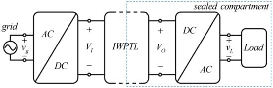
Figure 1.
Wireless power delivery system based on SS-compensated IWPTL.
The rest of the paper is organized as follows. Series-series compensated IWPT link is analyzed in Section 2, presenting phasor domain solution and time-domain solution alongside the theory of LIVO operation. Relations between primary DC-side quantities to primary and secondary AC-side phasors are revealed in Section 3. An example of the proposed method application is described in detail in Section 4. The paper is summarized in Section 5.
2. SS-Compensated IWPT Link Essentials
2.1. The Circuitry
Consider an SS-compensated IWPTL, shown in Figure 2, with VI and VO denoting input and output dc voltages, L1 and L2 symbolizing primary and secondary inductances, C1 and C2 representing primary and secondary compensating capacitances, r1 and r2 signifying equivalent primary and secondary equivalent series resistances, k indicating coupling coefficient, CI and CO standing for input and output filter capacitances and RO denotes equivalent load resistance, respectively. The inverter is operated with 50% duty cycle at constant frequency ω = 2π∙f, thus that inverter output voltage
is a bipolar square-wave signal with V1n denoting nth harmonic magnitude. Primary-side current is given by
with I1n and φn denoting nth harmonic magnitude and phase, respectively. The resonant frequency of the system ωR is given by
and secondary-side variables are described by
with V2n, I2n and θn, δn denoting nth secondary voltage and current harmonic magnitudes and phases, respectively.
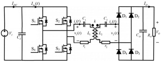
Figure 2.
SS-compensated IWPT link.
The IWPT link may be represented in phasor-domain by its first-harmonic equivalent circuit (FHEC) shown in Figure 3 [5] with
and equivalent AC-side load [9]

Figure 3.
Equivalent phasor-domain circuit.
Denoting
Figure 3 suggests that phasor domain solution of secondary AC-side variables may be derived as
Representing voltage and current phasors as a sum of in-phase (real) and quadrature (imaginary) components
respectively, and substituting into Equation (8) yields
Considering Equations (6) and (9), AC-side voltage and load impedance components are then given by
2.2. LIVO Operation
LIVO frequencies (imposing load-independent voltage gain Equation (12)) can be calculated by forcing the load-related component in Equation (12) to zero, i.e.,
Neglecting equivalent series resistances and brings Equation (13) to
Two LIVO frequencies and are identified by solving Equation (14) using Equations (4) and (7) as
with residing below resonance (capacitive region) and belonging to the inductive region above resonance, i.e., . Inductive region frequency is typically used for LIVO operation, allowing a lower harmonic distortion of primary and secondary currents and natural zero voltage switching (ZVS) of inverter valves, and is considered in this paper. In order to derive load impedance components in Equation (11), the time-domain solution of the circuit in Figure 2 is necessary, carried out in the following subsection.
2.3. Equivalent Input Impedance of Diode Rectifier Operating in CCM
Operation at yields (neglecting equivalent series resistances and ) θ1 = 0 (see [12] for details). Time-domain behavior of the IWPTL in Figure 2 is then described by the following system of differential equations,
with uC1, uC2 denoting instantaneous voltages across primary and secondary capacitances, respectively, and initial conditions given by
and
Solving Equation (17) with (18) yields [14]
with
denoting the output DC-side current of the IWPT link. Observing Equation (19), it may be concluded that although IWPT link operation frequency is , both current contains a term at lower LIVO frequency as well. Since in general is not a multiple of , the term at lower LIVO frequency may contribute to both active and reactive components. Hence, when calculating phasor domain components of secondary current, it is necessary to utilize Fourier decomposition of Equation (19) thus that
On the other hand, secondary side voltage phasor may be expressed as
Equivalent input impedance of the diode rectifier is typically considered as series-connected resistance and reactance (Figure 4a), calculated from Equations (6) and (11). However, it may also be expressed by parallel-connected resistance and reactance (Figure 4b). Noticing that
there are
and
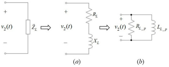
Figure 4.
Equivalent load impedance circuit: (a) series form, (b) parallel form.
It may be concluded from Equation (25) that for a known secondary side inductance L2 and coupling coefficient k, inductance is both well defined and load-independent.
3. Input DC-Side Quantities-Based Estimation Method
3.1. Primary AC-Side Variables in-Phase Components Derivation
The first harmonic in-phase component of the inverter output voltage is related to input DC voltage as
Moreover, inverter input current iin(t) is related to inverter output current i1(t) as (see Figure 5)
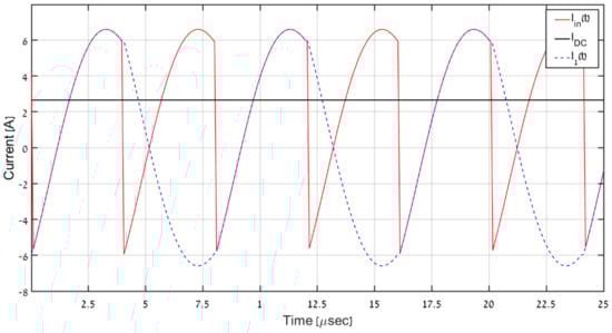
Figure 5.
Primary-side current shapes of a LIVO-operating IWPT.
On the other hand, input DC-side current of the IWPT link IDC is given by
Consequently, the first harmonic in-phase component of primary AC-side current is obtained as
3.2. Estimation of Output DC-Side Voltage and Resistance Utilizing Input DC-Side Variables in CCM
Using Equations (10), (26), (28), and (29), secondary AC-side output voltage is given by
i.e., quadrature component of primary AC-side current can be expressed as
Furthermore, substituting Equations (22), (25), and (31) into (10) yields
with
It may be concluded that primary and secondary AC-side voltage and current components may be obtained utilizing primary DC-side variables VI and IDC only. In case the diode rectifier operates in continuous conduction mode (CCM), combining the solution of Equation (32) with Equation (11) yields [9,18]
with PO denoting DC-side output load power of the system.
3.3. Correction for DCM Regime
Operation at in CCM while neglecting equivalent series resistances and yields) cf. (12)–(15)) [17]
However, parasitic resistances and are nonzero in practice. Moreover, as mentioned above, the linear relation between secondary AC and DC side variables Equation (34) is only valid in case the diode rectifier operates in CCM and does not hold in DCM. As presented in [19], the imaginary part of the diode rectifier input impedance possesses inductive characteristics, which are relatively insignificant in CCM (and may thus be neglected [14]) but rise significantly in DCM. Moreover, IWPT currents possess significant harmonic content in the DCM regime thus that the FHEC (Figure 3) is no longer accurate. Consequently, operation at or does not result in LIVO in practice. It was demonstrated in [17] that SS-compensated IWPTL output voltage at LIVO frequency is given by
with
where PO denotes the load power, PO,B signifies load power level corresponding to the bound between CCM and DCM, PO,MIN represents minimum allowed IWPTL load power [20] and VO,B and VO,MAX symbolize output DC-side voltages corresponding to PO,B and PO,MIN, respectively. It is well-evident that neglecting patristics resistances and reduces the first row of Equation (36) (corresponding to CCM) to Equation (35). On the other hand, the relation between the output voltage and load power relation is highly nonlinear yet well-defined analytically in DCM regime (second row of Equation (36)). Nevertheless, the relation between the rows of Equation (36) is injective (one-to-one), and hence DCM-related output voltage may be estimated from its corresponding CCM counterpart. The relation between the load resistance value and the load power may be obtained by substituting (36) into
4. Example
Consider the 1 kW SS-compensated IWPT link shown in Figure 2 with parameter values summarized in Table 1, operating at LIVO frequency . According to Table 1, resonant and operating frequencies of the IWPT link are
respectively. The IWPT link is designed to be utilized for delivering power into an enclosed compartment through 10 mm-thick polyvinyl-chloride plate (see Figure 6) with near-unity voltage gain. The transmitter-side inverter is realized by modified Transphorm TDINV1000P100-KIT 1-kW Inverter GaN Evaluation Platform (Transphorm, Goleta, CA, USA) [21] utilizing 650 V, 150 mΩ TPH3206PSB gallium-nitride field-effect transistors (Transphorm, Goleta, CA, USA) driven by silicon labs SI8273AB1 isolated drivers (Skyworksinc, Irvine, CA, USA). Switching signals are generated by Texas Instrument TMS320F28335 digital signal processor (Texas Instruments, Dallas, TX, USA). The diode rectifier is formed by four Microsemi APT40DQ120BG devices. The system is fed from IT61517D ITECH high-voltage DC power supply (ITECH, New Taipei City 23586, Taiwan) and loaded by Maynuo M9715 DC (Maynuo, Nanjing, Jiangsu 20019, China) electronic load, functioning in constant-power mode. IWPT link DC output is terminated by a 20 kΩ resistor to realize the minimum allowed load of PO,MIN = 9 W [20].

Table 1.
System Parameter Values.

Figure 6.
Experimental setup.
Output voltage and load resistance versus load power curves were derived experimentally in [18] and are reproduced in Figure 7 and Figure 8, respectively. The output voltage versus load power relation of the system is given by
corresponding to (36) with VO,B = 395 V, VO,MAX = 428 V, PO,B = 250 W and PO,MIN = 9 W. Due to the fact that CCM is assumed for the phasor domain solution Equation (10), IWPT link output voltage would be given by the first row of Equation (40) all load levels. In order to include a nonlinear correction to allow accurate estimation of VO in DCM,
yields the final IWPT link output voltage estimate for all feasible load levels.
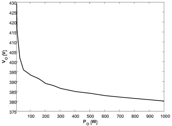
Figure 7.
Measured output voltage versus load power [19].
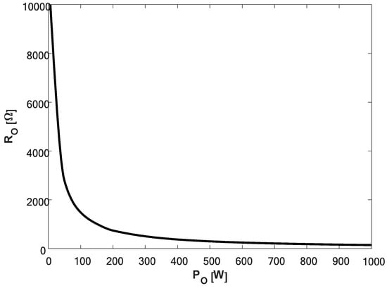
Figure 8.
Measured load resistance versus load power [19].
According to Equations (38) and (40), there is
Again, CCM is assumed for the phasor domain solution Equation (10) and hence IWPT link output resistance would be given by the first row of Equation (42) for all load levels. In order to perform a nonlinear correction to allow accurate estimation of RO in DCM,
with signifying load resistance corresponding to diode rectifier operation on the bound between CCM and DCM yields the final IWPT link output resistance for all feasible load levels.
4.1. Simulations
In order to validate the proposed DC-side measurement-based estimation methodology, the system was simulated with input DC-side variables employed as real-time inputs to the proposed secondary AC-side estimator (32). Simulated AC-side variables were compared to estimated ones (recognized by superscript ‘est’ from now on). Time-domain AC-side waveforms for different load levels (1000 W and 600 W corresponding to CCM regime and 200 W, 100 W, and 50 W imposing DCM regime) are shown in Figure 9, Figure 10, Figure 11, Figure 12 and Figure 13 where V1, I1, V2, I2 denote primary and secondary AC-side voltages and currents, respectively; V1h1, I1h1, V2h1, I2h1 symbolize corresponding first-harmonic components (obtained by band-pass filtering of V1, I1, V2, I2 around operation frequency), and V11, I11, V21, I21 with α1, ϕ1, θ1, δ1 signify estimated phasor component values calculated using (32) and (11). It is well-evident that CCM operation imposes continuous secondary currents and the square-wave secondary voltage, as expected. On the other hand, the discontinuous nature of secondary current and distortion of secondary voltage during the non-conduction period is clearly visible in DCM.

Figure 9.
Simulation results, PO = 1000 W.
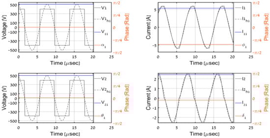
Figure 10.
Simulation results, PO = 600 W.
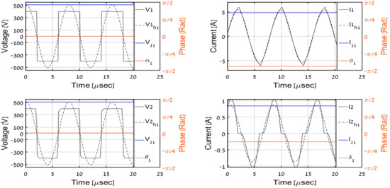
Figure 11.
Simulation results, PO = 200 W.
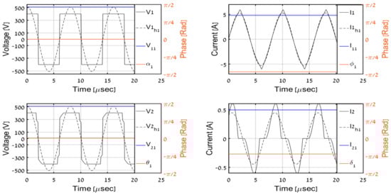
Figure 12.
Simulation results, PO = 100 W.
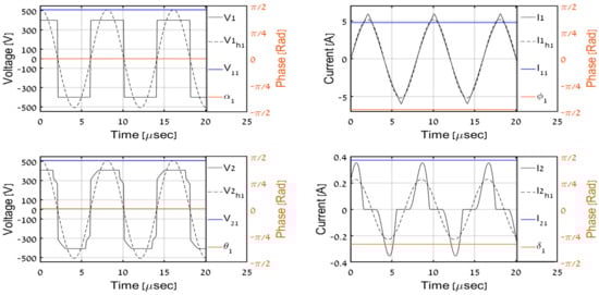
Figure 13.
Simulation results, PO = 50 W.
Observing the results, it may be concluded that the methodology results in accurate prediction of the first harmonic components of primary-side variables and their secondary-side counterparts for all load levels. Then, (34), (41), and (43) are applied to estimate the output DC-side voltage and resistance based on secondary AC-side estimations. Table 2 summarizes the estimation algorithm performance. It may be concluded that estimated values of output voltage and resistance are satisfactory to indicate the correct operation of the system, which is the major goal of the proposed process.
Table 2.
Simulation results summary.
4.2. Experiments
In order to experimentally validate the proposed methodology, the system in Figure 6 was operated under multiple load levels (including those during simulations). All AC-side and DC-side variables were acquired during experiments. Then, recorded input DC waveforms were applied to (32) in an offline manner to obtain corresponding estimations and compare them to their measured counterparts. Time-domain AC-side waveforms for load levels matching the simulations are shown in Figure 14, Figure 15, Figure 16, Figure 17 and Figure 18, respectively. It is well-evident that estimated phasor components match well with corresponding first harmonic waveforms. Table 3 summarizes the estimation algorithm performance.
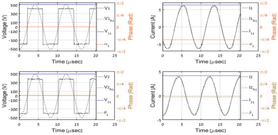
Figure 14.
Experimental results, PO = 1000 W.

Figure 15.
Experimental results, PO = 600 W.
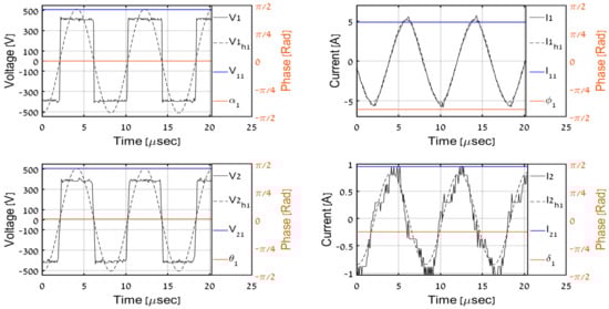
Figure 16.
Experimental results, PO = 200 W.
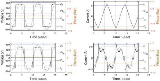
Figure 17.
Experimental results, PO = 100 W.
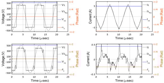
Figure 18.
Experimental results, PO = 50 W.
Table 3.
Experimental results summary.
It should be emphasized that DCM secondary current waveforms are somewhat different from their simulation counterparts. This is due to the fact that the simulation model does not include parasitic capacitances of the coils and the diode bridge since they do not affect the first harmonic behavior. In general, if parasitics are brought into the model, the results look much more similar [20]. Here, the first harmonics only are of interest, and it is shown that the first harmonic approximations are quite similar in simulations and experiments.
In order to further validate algorithm performance, Figure 19 and Figure 20 graphically demonstrate estimated values of output load values and load resistance, respectively, versus corresponding measurements for the whole load power levels range. Recalling that the estimation process is used for monitoring and protection rather than for feedback control, the obtained accuracy may be considered satisfactory.

Figure 19.
IWPT link measured and estimated output DC voltage versus load power.
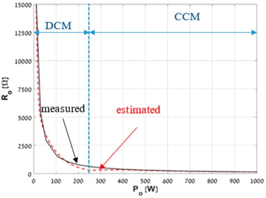
Figure 20.
IWPT link measured and estimated output resistance versus load power.
5. Conclusions
Input DC-side variables-based methodology is proposed for estimation of the output voltage and resistance of IWPT link with known coupling coefficient, operating at LIVO frequency. The time-domain solution contributes the necessary additional equation to describe the system in addition to the commonly used phasor domain equation. The proposed approach yields highly accurate results in the CCM regime yet requires a nonlinear correction in DCM region. Compared to other methods used for output voltage and resistance estimation, the proposed approach uses a simpler and lower-cost solution. The outcomes were supported by simulations and experiments. Future work on the subject may focus on accuracy improvement of the method and adoption of different artificial intelligence methods [22,23,24,25,26] to perform the task.
Author Contributions
Conceptualization, O.T. and A.K.; methodology, O.T. and A.K.; software, O.T.; validation, O.T.; formal analysis, O.T. and A.K.; investigation, O.T.; resources, A.K.; writing—original draft preparation, O.T.; writing—review and editing, A.K.; supervision, A.K.; funding acquisition, A.K. All authors have read and agreed to the published version of the manuscript.
Funding
This research received no external funding.
Conflicts of Interest
The authors declare no conflict of interest.
Abbreviations
| SS | series-series |
| IWPT | induction wireless power transfer |
| IWPTL | induction wireless power transfer link |
| LIVO | load independent voltage output |
| CCM | continuous conduction mode |
| DCM | discontinuous conduction mode |
| RMS | root-mean-square |
| FHEC | first harmonic equivalent circuit |
| EV | electric vehicle |
| ZVS | zero voltage switching |
References
- Zhang, Z.; Pang, H.; Georgiadis, A.; Cecati, C. Wireless power transfer—An overview. IEEE Trans. Ind. Electron. 2019, 66, 1044–1058. [Google Scholar] [CrossRef]
- Mi, C.C.; Buja, G.; Choi, S.Y.; Rim, C.T. Modern advances in wireless power transfer systems for roadway powered electric vehicles. IEEE Trans. Ind. Electron. 2016, 63, 6533–6545. [Google Scholar] [CrossRef]
- Hu, S.; Liang, Z.; Wang, Y.; Zhou, J.; He, X. Principle and application of the contactless load detection based on the amplitude decay rate in a transient process. IEEE Trans. Power Electron. 2017, 32, 8936–8944. [Google Scholar] [CrossRef]
- Meng, X.; Qiu, D.; Lin, M.; Tang, S.C.; Zhang, B. Output voltage identification based on transmitting side information for implantable wireless power transfer system. IEEE Access 2018, 7, 2938–2946. [Google Scholar] [CrossRef]
- Miller, J.M.; Onar, O.C.; Chinthavali, M. Primary-side power flow control of wireless power transfer for electric vehicle charging. IEEE J. Emerg. Sel. Top. Power Electron. 2015, 3, 147–162. [Google Scholar] [CrossRef]
- Li, S.; Hui, S.Y.R. Comparative study on front-end parameter identification methods for wireless power transfer without wireless communication systems. In Proceedings of the International Power Electronics Conference (IPEC-Niigata 2018-ECCE Asia), Niigata, Japan, 20–24 May 2018. [Google Scholar]
- Wang, Z.-H.; Li, Y.-P.; Sun, Y.; Tang, C.-S.; Lv, X. Load detection model of voltage-fed inductive power transfer system. IEEE Trans. Power Electron. 2013, 28, 5233–5243. [Google Scholar] [CrossRef]
- Chow, J.P.-W.; Chung, H.S.-H.; Cheng, C.-S. Use of transmitter-side electrical information to estimate mutual inductance and regulate receiver-side power in wireless inductive link. IEEE Trans. Power Electron. 2016, 31, 6079–6091. [Google Scholar] [CrossRef]
- Mohammad, M.; Choi, S. Sensorless estimation of coupling coefficient based on current and voltage harmonics analysis for wireless charging system. In Proceedings of the IEEE Energy Conversion Congress and Exposition (ECCE), Cincinnati, OH, USA, 1–5 October 2017. [Google Scholar]
- Madawala, U.K.; Thrimawithana, D.J. New technique for inductive power transfer using a single controller. IET Power Electron. 2012, 5, 248–256. [Google Scholar] [CrossRef]
- Sun, L.; Sun, M.; Ma, D.; Tang, H. Detecting load resistance and mutual inductance in series-parallel compensated wireless power transfer system based on input-side measurement. Int. J. Antennas Propag. 2018, 2018, 2094637. [Google Scholar] [CrossRef]
- Frechter, Y.; Kuperman, A. Output voltage range of a power-loaded series-series compensated inductive wireless power transfer link operating in load-independent regime. IEEE Trans. Power Electron. 2020, 35, 6586–6593. [Google Scholar] [CrossRef]
- Trachtenberg, O.; Kuperman, A. Quadrature demodulator-assisted estimation of load voltage and resistance based on primary-side information of a wireless power transfer link. Electronics 2021, 10, 1858. [Google Scholar] [CrossRef]
- Costanzo, A.; Dionigi, M.; Mastri, F.; Mongiardo, M.; Monti, G.; Russer, J.A.; Russer, P.; Tarricone, L. Conditions for a load-independent operating regime in resonant inductive WPT. IEEE Trans. Microw Theory Technol. 2017, 65, 1066–1076. [Google Scholar] [CrossRef]
- Zhang, W.; Wong, S.; Tse, C.K.; Chen, Q. Analysis and comparison of secondary series- and parallel-compensated inductive power transfer systems operating for optimal efficiency and load-independent voltage-transfer ratio. IEEE Trans. Power Electron. 2014, 29, 2979–2990. [Google Scholar] [CrossRef]
- Trachtenberg, O.; Baimel, D.; Kuperman, A. Accurate first-harmonic-approximation-based model of the diode rectifier in series-series compensated inductive wireless power transfer link at load-independent-voltage-output frequency. Int. J. Electron. Commun. 2021, 135, 153732. [Google Scholar] [CrossRef]
- Frechter, Y.; Kuperman, A. Analysis and design of inductive wireless power transfer link for feedbackless power delivery to enclosed compartment. Appl. Energy 2020, 278, 115743. [Google Scholar] [CrossRef]
- Wang, C.S.; Covic, G.A.; Stielau, O.H. Power transfer capability and bifurcation phenomena of loosely coupled inductive power transfer systems. IEEE Trans. Ind. Electron. 2004, 51, 148–157. [Google Scholar] [CrossRef]
- Trachtenberg, O.; Shoihet, A.; Beer, E.; Fux, E.; Tiktin, N.; Kolesnik, S.; Kuperman, A. Quadrature demodulator based output voltage and load estimation of a resonant inductive WPT link. In Proceedings of the IEEE PELS Workshop on Emerging Technologies: Wireless Power Transfer (WoW), London, UK, 17–21 June 2019. [Google Scholar]
- Frechter, Y.; Kuperman, A. On the minimal loading of sensorless series-series compensated inductive WPT link operating at load independent voltage output frequency without feedback. IEEE Access 2020, 8, 192517–192526. [Google Scholar] [CrossRef]
- 1kW Inverter GaN Evaluation Platform. Available online: https://www.transphormusa.com/en/evaluation-kit/tdinv1000p100-kit/ (accessed on 18 July 2021).
- Ju, X.; Chen, V.; Rosenberger, J.; Liu, F. Fast knot optimization for multivariate adaptive regression splines using hill climbing methods. Expert Syst. Appl. 2021, 171, 114565. [Google Scholar] [CrossRef]
- Prado, D.; Lopez-Fernandez, J.; Arrebola, M. Systematic Study of the Influence of the Angle of Incidence Discretization in Reflectarray Analysis to Improve Support Vector Regression Surrogate Models. Electronics 2020, 9, 2105. [Google Scholar] [CrossRef]
- El Morabit, S.; Rivenq, A.; Zighem, M.-E.-N.; Hadid, A.; Ouahabi, A.; Taleb-Ahmed, A. Automatic Pain Estimation from Facial Expressions: A Comparative Analysis Using Off-the-Shelf CNN Architectures. Electronics 2021, 10, 1926. [Google Scholar] [CrossRef]
- Liu, F.; Ju, X.; Wang, N.; Wang, L.; Lee, W.-J. Wind farm macro-siting optimization with insightful bi-criteria identification and relocation mechanism in genetic algorithm. Energy Convers Manag. 2020, 217, 112964. [Google Scholar] [CrossRef]
- Ju, X.; Liu, F. Wind farm layout optimization using self-informed genetic algorithm with information guided exploitation. Appl. Energy 2019, 248, 429–445. [Google Scholar] [CrossRef]
Publisher’s Note: MDPI stays neutral with regard to jurisdictional claims in published maps and institutional affiliations. |
© 2021 by the authors. Licensee MDPI, Basel, Switzerland. This article is an open access article distributed under the terms and conditions of the Creative Commons Attribution (CC BY) license (https://creativecommons.org/licenses/by/4.0/).