Abstract
By using a mixer to down-convert the high frequency components of a signal, digital bandwidth interleaving (DBI) technology can simultaneously increase the sampling rate and bandwidth of the sampling system, compared to the time-interleaved and hybrid filter bank. However, the software and hardware of the classical architecture are too complicated, which also leads to poor performance. In particular, the pilot tone used to synchronize the analog and digital local oscillators (LO) of mixers intermodulates with the high frequency components of the signal, resulting in larger spurs. This paper proposes a synchronous mixing architecture for the DBI system, where the LO of the analog mixer is synchronized with the sampling clock of the analog-to-digital converter. Its hardware and software are simplified—the pilot tone used to synchronize the LOs can also be removed. An evaluation platform with a sampling rate of 250 MSPS is implemented to illustrate the performance of the new architecture. The result shows that the spurious free dynamic range (SFDR) of the new architecture is more than 20 dB higher than the classical one in a high frequency range. The rise time of a step signal of the new architecture is 0.578 ± 0.070 ns faster than the classical one with the same bandwidth (90 MHz).
1. Introduction
The demand for sampling systems with a higher bandwidth and sample rate has dramatically increased for such fields as software-defined radio, coherent optical communication and time domain measurement [1,2,3]. However, due to the limitation of semiconductor technology, it is difficult to increase the speed of an analog-to-digital converter (ADC) above a gigahertz, which limits the sample rate of the sampling system [4,5].
The concept of time-interleaved ADCs was first proposed for increasing the speed of the sampling systems [6]. In the time-interleaved systems, ADCs are connected in parallel at the front end while sampling at different phases of the same clock. The digital multiplexer driven by ADCs sequentially selects the output of each channel to obtain the full speed code. The time-interleaved sampling system is extremely sensitive to the mismatches between the sub-ADCs. The signal-to-noise ratio (SNR) and spurious free dynamic range (SFDR) are not as good as a system that is built up with a single ADC [7,8]. The mismatches include offset, gain and sample time skew; some papers analyze the mismatch effects in a time-interleaved system and introduce some compensation methods, divided into foreground and background calibrations [9,10,11]. The normal operation of the ADC is interrupted during the foreground calibration, which is usually performed when the system is powered on. The background calibration does not affect the normal operation of the ADC.
Another popular architecture for parallelizing ADCs is proposed in [12], which is called hybrid filter bank (HFB). It uses an analog analysis filter bank to replace the input power divider (or driver amplifier) in a time-interleaved system. It reconstructs the signal through a digital filter bank instead of a multiplexer. The analog analysis filter bank allocates different frequency bands to each sub-ADC, and attenuates the aliasing caused by the mismatch. Compared with the time-interleaved system, it greatly reduces the sensitivity of performance to mismatches between converters.
The two methods introduced above both increase the system sampling rate, but cannot increase the bandwidth. Its upper limit is still determined by a single converter. The ADCs in the time-interleaved and hybrid filter bank architectures need to operate in the second Nyquist zone or even higher. Most gigahertz converters do not have this capability. Therefore, a series of frequency-interleaved architectures that use mixers to down-convert the input signal have been proposed [3,13,14,15,16,17,18,19]. They can be divided into two categories: one is similar to time-interleaved ADCs, where the input signal is first distributed to each channel by a power divider and then down-converted by a mixer, which is generally a complex mixer [13,15,17,18]; the other is similar to the HFB system, where the analog analysis filter bank allocates the input signal to the sub-channel, followed by down-conversion. Due to the high operating frequency, the analog filter bank is passive, and the mixer is also a real mixer with a simple structure [3,14,16,19].
The digital bandwidth interleaving (DBI) system that this article focuses on belongs to the second architecture. Some high-speed digital oscilloscopes use DBI technology, which connects multiple acquisition channels in parallel while increasing both bandwidth and sampling rate [3,14,16]. Some problems still exist in the classical DBI system. First of all, the digital reconstruction process of the signal is too complicated, consumes too many computing resources, and cannot be completed in real time [3]. Secondly, it requires a pilot tone insertion system to establish the local oscillators (LO) synchronization between analog and digital mixers [20]. Pilot tone insertion requires analog circuits and digital LO synthesizers to work together, which increases hardware complexity and software calculations, and also leads to a decrease in the performance of the sampling system. Last but not least, the quality of the signal reconstructed by the DBI technology is not good, and there are many spurious components, which is worse than the time-interleaved system after calibration [21].
In this article, a new architecture called synchronous mixing for the DBI system is introduced. Compared with the classical architecture, it does not require digital mixing when reconstructing the signal, so there is no need to insert a pilot tone. In the synchronous mixing architecture, the signal reconstruction process is similar to the HFB system, and only a set of digital synthesis filters is needed, which can remove digital anti-aliasing filters in the classical DBI system. Although the software and hardware are greatly simplified, the reconstructed signal of the synchronous mixing architecture has a higher SFDR than the classical one because there is no intermodulation between the pilot tone and the input signal at the ADC drive amplifier.
The rest of this paper is organized as follows. In Section 2, the sampling and reconstruction process of the classical DBI system is briefly described. Section 3 discusses the problems existing in the classical DBI system. In Section 4, the synchronous mixing architecture is proposed for the DBI system. The platform for evaluating the performance of the two architectures is built in Section 5. Section 6 gives some test results and the discussion. Finally, the conclusions are drawn in Section 7.
2. Classical DBI Sampling System
A classical two-channel DBI sampling system is shown in Figure 1. The input signal is bandlimited to , and the output is a discrete-time sequence . and are the frequency responses of the analog analysis filter bank, which is usually realized by a diplexer. and are the frequency responses of the image rejection filter after the analog and digital mixers. and are the frequency responses of the interpolation filters. and are the frequencies of the reconstruction filters. In this section, it is assumed that the stopband attenuation of the image rejection and interpolation filter is large enough to completely eliminate the aliasing components.
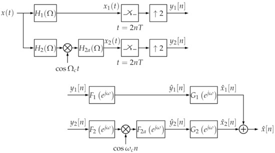
Figure 1.
Two-channel digital bandwidth interleaving (DBI) system.
As shown in Figure 2, a real diplexer has a crossover region between the low-pass and high-pass channel. We define the stopband frequency point of the low-pass channel as , where , . Similarly, we define and for the high-pass channel. The crossover region is the frequency range between and . The signal in this range is sampled by both channels at the same time. In order to simplify the analysis of the spectrum shifting by the mixer, we split the spectrum of the real signal into positive and negative bands as follows:
where is the Fourier transform of . Similarly, we define and . For digital filters, the range from to are the positive band, and the rest are the negative band, where k is an integer. The analog angular frequency and digital angular frequency satisfy , where is the total sampling rate of the DBI system.
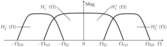
Figure 2.
Frequency response of input diplexer. is the low-pass channel, is the high-pass channel.
For the low frequency (LF) band, the output of diplexer is sampled with a period of , and then up-sampled by a factor of 2 to obtain . The discrete-time Fourier transform (DTFT) of the sequence is as follows:
We define that and are the extension of and with a period of , where and bandlimited to [22]. Therefore, Equation (2) can be written as follows:
In the classical DBI system, each sub-channel strictly satisfies the Nyquist sampling theorem, so is less than . in Equation (3) is the aliasing component caused by upsampling, which can be eliminated by the interpolation filter . Then, we have the following:
In Equation (4), is reserved because the interpolation filter is not an ideal low-pass filter, and there is attenuation in the passband.
For the high frequency (HF) band, in order for to satisfy the sampling theorem, is required. The local oscillator (LO) frequency is chosen to create high-side injection for reducing the spurs generated by the mixer; therefore, . The Fourier transform of is as follows:
The frequency of the digital mixer LO is . In order to prevent the image generated by digital mixing overlapping the original signal, must be met. So, the DTFT of is as follows:
where is given by the following:
The definitions of and are the same as that of . Finally, the output sequences of the high and low frequency bands are added together to produce . Its DTFT can be written as follows:
where
For a continuous time signal bandlimited to , when discretized by a single channel sampling system with a period of T, the DTFT of the output sequence is as follows [23]:
Comparing Equations (8) and (11), it can be concluded that when the reconstruction filters and are designed so that , the DBI system is equivalent to a single channel sampling system. Considering causality in physical realization, the system should have a delay , so the perfect reconstruction equation becomes as follows:
In DBI system, is bandlimited to and is bandlimited from to . Therefore, in the region , and need to meet the following:
In the crossover region,
where means the unwrapped phase response.
For more convenient implementation, and are divided into two stages in the actual DBI system [3], as shown in Figure 3. First, use and to correct the phase of the crossover region of the two channels to satisfy Equation (15). Then add the outputs together, and use to compensate the full frequency band amplitude and phase. Furthermore, the total delay of the low frequency channel is shorter, and have eliminated the alias. Therefore, in [19], let be a cascade of a fixed delay and digital infinite impulse response (IIR) all-pass filter and to simplify the implementation. In addition, the frequency-independent factors in Equations (9) and (10) are compensated by adjusting the ADC drive amplifier, which adds less of a noise floor than the digital compensation.
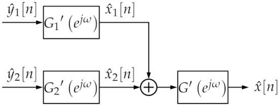
Figure 3.
Realization of and in classical DBI system for two stages.
3. Problems of Classical Architecture
The classical DBI architecture can increase the sampling rate and bandwidth at the same time, but there are still some problems. This section describes them in detail. First of all, it requires a very large amount of calculation. As shown in Figure 1, there are five digital filters in a two-channel DBI system. Among them, filters , and are used to eliminate the image generated after interpolation or mixing. In order not to add a non-linear phase, generally, a linear phase finite impulse response (FIR) filter is used. The order N of low-pass FIR filter can be estimated according to the Kaiser formula as follows [24]:
and in Equation (16) are the ripples in the pass and stop band, respectively, and is the normalized (by the sampling rate) width of the transition band. When we use a high speed 8-bit ADC, we can generally let , and , so the order of each FIR filter is . Ten years ago, the highest speed DBI system sampling rate was 80 GS/s [16]. At this rate, only the digital signal processing (DSP) performance required to implement the above three filters is 110 TMAC/s. The field programmable gate array (FPGA) with the highest DSP capability now has a performance of no more than 22 TMAC/s [25]. Therefore, the real-time processing of each sampling point is completely impossible in the classic DBI system.
The DBI system usually uses a central processing unit (CPU) for the digital signal processing, and with an advanced trigger system, only a short sampling sequence after the trigger time is reconstructed and processed. As shown in Figure 4, the trigger time is generally random, and in the high frequency channel, it corresponds to the different phase of the analog LO. Therefore, it is difficult to determine the LO phase of digital mixing during reconstruction.
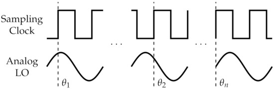
Figure 4.
Different analog LO phases at different trigger times.
The classical DBI system uses a pilot tone insertion system to establish the synchronization between analog and digital LOs, as shown in Figure 5. This system includes analog and digital parts. In the analog domain, the analog LO and the sampling clock are multiplied by factors N and M from the same reference clock, and the value of the factor is determined according to different system requirements. The analog LO is divided into paths: one is to drive the mixer, and the other is divided by two. The divided LO passes through a band pass filter to eliminate harmonics and is inserted into the high frequency signal channel as a pilot tone. The high frequency input signal is down-converted by a mixer. The image is removed by a low-pass filter, and then passed through a band-stop filter with the same center frequency with pilot tone to eliminate the interference that may affect the subsequent pilot tone extraction in the digital domain. The down-converted signal and pilot tone are combined by the power combiner, then drive the ADC through the amplifier.
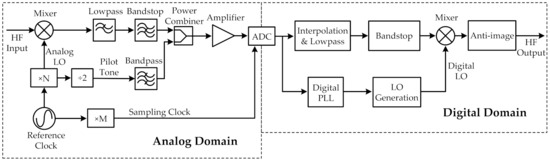
Figure 5.
Pilot tone insertion system.
In the digital domain, the sampling sequence is divided into two paths. One passes though the digital phase-locked loop (PLL) to obtain the phase information of the pilot signal, which is multiplied by 2 to obtain the phase of the analog LO, and then this phase is used to generate the digital LO. The other is interpolated and filtered by a low pass filter, and then a band stop filter is used to completely eliminate the pilot signal. Finally, the signal is up-converted by a digital mixer and anti-imaged to obtain the high frequency channel output. The digital PLL is realized by discrete Fourier transform (DFT), and its time complexity is , where L is the sequence length. Increasing L can improve the frequency resolution, but it leads to a rapid increase in the computational complexity.
In summary, the pilot tone insertion system is very complicated. At the same time, it also affects system performance and reduces the SFDR of the DBI system. In actual analog circuits, devices such as amplifiers, samplers and power combiners are not perfectly linear, and the value of 1 dB compression point is usually used to express its linear range [26]. The addition of the pilot tone reduces the range of the available linear interval of the high frequency channel. During the system’s single tone signal test, the pilot tone and input signal are intermodulated in the power combiner, amplifier and the sampler of ADC to generate spurs and reduce the SFDR of the system.
4. Synchronous Mixing Architecture
In this section, the synchronous mixing architecture for DBI system is described in detail. Synchronous mixing means that the LO for mixer in high frequency channel is the same as the sub-channel sampling clock. In this architecture, the digital mixer for upconversion and the pilot tone insertion circuit for the synchronization of the analog and digital LO can be removed. First, we will explain why the digital mixer can be removed in the synchronous mixing architecture. Then, the reconstruction process of the signal is analyzed in detail. It is similar to a HFB system.
The sampler can be represented as a multiplier and a continuous-to-discrete-time converter cascade, as shown in Figure 6. The input signal and a periodic impulse train are multiplied to obtain the following:
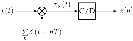
Figure 6.
Block diagram of an ideal sampler. C/D is a continuous-to-discrete-time converter.
Its Fourier transform is as follows:
Equation (11) is the DTFT of . It can be concluded from Equations (11) and (18) that the sampling process uses a periodic impulse train to modulate the input signal and then normalizes the frequency axis.
An ideal periodic impulse train has an infinite number of harmonics, and modulation replicates the signal spectrum for an infinite number of times, as shown in Figure 7. We usually only pay attention to the baseband signal after sampling and extract it through a low-pass filter during recovery. Similarly, we can also design various types of band-pass filters to recover the signals mixed by various harmonics. In the digital domain, we can use interpolation and high-pass filters to reconstruct the signal in the corresponding frequency band. For example, if we want to determine the mixed signal of sampling clock , we can interpolate the sequence by a factor of 2, and then pass it through a high-pass filter with a bandwidth of .
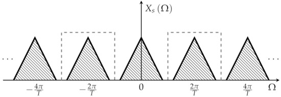
Figure 7.
Signal spectrum after impulse modulation. The frequency bands in the dashed box are of interest after sampling in the synchronous mixing architecture.
According to the above analysis, in the DBI system, we can use the sampler to upconvert, and then the digital mixer can be removed. In the high frequency band, we use synchronized clock signals to drive the analog mixer and ADC, which are the synchronized modulator and demodulator. Removing the digital mixer and anti-aliasing filter, the simplified DBI system is shown in Figure 8.
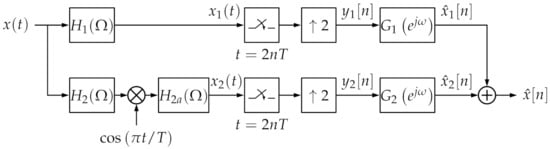
Figure 8.
Synchronous mixing DBI system.
Now, we analyze how to design the correct reconstruction filters for the synchronous mixing DBI system. For the low frequency band, only the low-pass filter after interpolator is removed, so the DTFT of still satisfies Equation (3). For the high frequency band, before , only the LO of analog mixer becomes , so the DTFT of is as follows:
where
Then, using the periodicity of the sampled signal, we have the following:
Finally, the sequences of two channels are added to obtain , and its DTFT should satisfy the following:
Therefore, and should satisfy the following:
where
Equation (23) is similar to the perfect reconstruction (PR) equation in the HFB system [22], where is called the distortion function, and is called the aliasing function. The distortion function represents the amplitude and phase response of the entire system, and the aliasing function represents the aliasing caused by the input signal at the image frequency point.
After we obtain the frequency response of the analog front-end circuit, we can refer to the design method of the synthesis filter bank in the HFB system to design and [27]. First, we solve Equation (23) at N equally spaced frequency points, then use inverse discrete Fourier transform (IDFT) to obtain the coefficients of the FIR filter. Finally, the coefficients are truncated by the appropriate window to obtain a filter of the specified length. is generally set to half of the length of the filter, and the value could be optimized by the Nelder–Mead simplex method in MATLAB [12]. The method of obtaining the response of the analog front-end circuit is given in Section 5.
5. Evaluation Platform and Methods
An evaluation platform is implemented in order to compare the performance of classical and synchronous mixing architectures, as shown in Figure 9. It can be divided into four parts: radio frequency (RF) front-end, data acquisition, digital signal processing and clock generation. The RF front-end includes the mixer, diplexer and other filters. Active mixer AD831 (manufactured by Analog Devices Inc., Norwood, MA, USA) is used for down-conversion of the high frequency signal. In order to reduce the harmonics generated by the mixer, there is a lumped resistance attenuator with 20 dB attenuation before it.
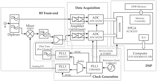
Figure 9.
Block diagram of the evaluation platform.
As shown in Figure 10, the input diplexer is implemented by connecting two singly terminated 11th-order Chebyshev low-pass and high-pass filters in parallel. The singly terminated filters are designed in the ADS (Advanced Design System) software. The diplexers are implemented using LQW series inductors and GRM series capacitors from Murata Company and assembled on double-layer printed circuit boards. Other analog filters are also implemented in this way. This type of diplexer is called a contiguous diplexer because the low-pass and high-pass filters have a common 3 dB attenuation frequency [28]. In physical realization, due to the insertion loss of the lumped capacitor and inductor, the attenuation of the common frequency is generally greater than 3 dB. Additionally, due to the finite quality (Q) factor of the component, the stopband attenuation is also limited. This article defines a gain less than −50 dB as the stopband. Some key specifications of the diplexers for classical and synchronous mixing architectures are shown in Table 1.
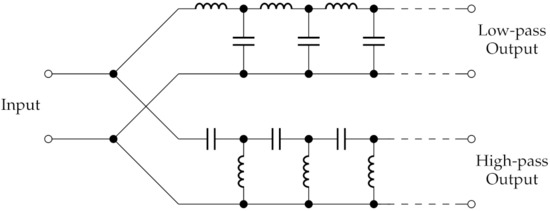
Figure 10.
Structure of the diplexer.

Table 1.
Key specifications for input diplexers.
Each 14-bit resolution ADC (ADC14X250) is driven in a cascade by a single-ended to differential amplifier (LMH5401) and a variable gain amplifier (LMH6401). Variable gain amplifiers are used to balance the gain difference between low-frequency and high-frequency channels. The total sampling rate of the system is 250 MSPS, so each ADC works at 125 MSPS. The sampling clock of ADCs is generated by PLL1 (LMK04828), which is driven by a programmable oscillator (LMK61E2), and the reference clock is 12.5 MHz. PLL1 also generates a logic clock for FPGA (XC7K325T-FFG900, manufactured by Xilinx Inc., San Jose, CA, USA) and drives PLL2 (LMX2572) and PLL3 (LMX2572) to generate the pilot tone (only for the classical architecture) and analog LO. All clocks are controlled and synchronized by PLL1. The ADCs, amplifiers, PLLs and reference clock are all manufactured by Texas Instruments Inc (Dallas, TX, USA).
LMK04828 is a phase-locked loop chip that complies with the JESD204B standard. It phase locks to the reference clock and generates the device clock and SYSREF signal (a signal used for synchronization of multiple converters defined in the JESD204B standard). In addition, the reference clock buffer in LMK04828 outputs the reference clock to a multiple output buffer LMK00304, which drives two secondary phase-locked loops LMX2572 to generate the analog LO and pilot tone, respectively. The SYNC and SYSREF signal are generated by the same frequency divider circuit in the LMK04828. It can not only control the synchronization of two LMX2572 chips, but also synchronize the ADC sampling clock and the analog LO. In the classical architecture, the analog LO is set to 95 MHz. In the synchronous architecture, the analog LO is the same as the single ADC sampling clock at 125 MHz.
Data are transferred between ADC and FPGA through the JESD204B interface, and then sent to the DDR memory (MT41K256M16TW, manufactured by Micron Inc., Boise, Idaho, USA) for buffering. The JESD204B core and the memory controller in the FPGA are connected by the AXI4-Stream bus, and data transmission is carried out through direct memory access. The computer obtains data through communication between the Vivado software on the computer and the Integrated Logic Analyzer (ILA) on FPGA. FPGA is only responsible for the synchronous reception and buffering of ADC sampled data. Digital filtering, digital mixing, pilot tone phase extraction and data reconstruction are all done on the computer using MATLAB software. For the classic architecture, , and are designed using the Filter Designer toolbox. The key specifications of them are as shown in Table 2.
Table 2.
Key specifications for digital anti-alias filter in classical architecture.
The reconstruction filter design method of the classical DBI system is introduced in detail in [29]. For the synchronous mixing architecture, we need to know the analog front-end circuit frequency response and in order to design the reconstruction filters. We can use a series of tones of different frequencies to test the system, use DFT to analyze sequences and , and obtain the amplitude and phase of the sampling sequence at the corresponding frequency point [30]. According to Equations (3) and (21) (without considering alias components), we compare the sampling sequence with the original signal, and calculate and .
When using single tone test to obtain the system response, the sampling system under test should have a precise trigger circuit to determine the initial moment of the sequence so that the absolute phase response of the system can be obtained [31]. However, the system in this article does not include a trigger circuit. We design the reconstruction filter bank by obtaining the amplitude and relative phase response between the two channels through a single tone test, and then use the pulse signal test to adjust the overall phase response. We denote the amplitude response of the two channels as and , and the relative phase response as follows:
where and are absolute phase response of and . The frequency independent gain factors are compensated by the input amplifier of the ADCs. The total delay of the system is . We use , and to solve Equation (23) to obtain the reconstruction filter response as follows:
where
Using this filter bank to reconstruct the signal, the aliasing function of the system is as follows:
where
The distortion function of the system is as follows:
From Equations (28) and (30), it can be concluded that signal reconstruction using reconstruction filters designed through the amplitude response and relative phase response is also alias free, the amplitude is also not distorted, and it is only phase away from the perfect reconstruction. We can calibrate this phase difference by a pulse test because the entire system is low-pass, and the phase response is linear at a very low frequency. After the pulse signal is input to the system, the output sequences of reconstruction filters and are added together to obtain its DFT. We adjust the initial time of the sequence to make the phase of the fundamental wave the same as that of the input pulse, and then compare the phases of other harmonics to obtain the phase response to be compensated.
The system design using the perfect reconstruction equation has a brick wall response, and its Gibbs effect is very obvious. The actual sampling system response types include Gaussian, maximum flat and Bessel responses [32]. The maximum flat response has the smallest oversampling rate and is commonly used in high speed acquisition systems. Therefore, in the synchronous mixing architecture, a digital filter is added after the phase compensation filter to adjust the system to the maximum flat response. In summary, the reconstruction process of the synchronous mixing system is shown in Figure 11.
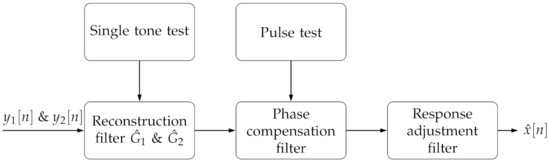
Figure 11.
Reconstruction process of the synchronous mixing architecture.
For the synchronous mixing architecture, a series of single tone tests with total of 200 frequency points are carried out. Then, 2048 points are obtained through spline interpolation to solve Equation (26) to obtain the response of the reconstruction filter. Finally, we use the inverse fast Fourier transform (IFFT) and rectangular window truncation to obtain 736 order FIR filters and . Increasing the order of the filter does not improve the reconstruction effect much. In the pulse test, the response value to be compensated can be added to and ; then, we use IFFT to solve the new and . The advantage of this is that there is no need to increase the order of the filter for phase compensation. The response compensation factor can be multiplied by in Equation (26), which means that a brick wall response system is not needed. The above method is also used to obtain in the classical architecture, as shown in Figure 3. The order of this filter is also 736.
Figure 12 shows the prototype system under test. The arbitrary waveform generator DG4162 from RIGOL Technologies is used to generate single tone signal and pulse signals. Two power supplies, GPE-2323C and GPD-3303S, from Good Will Instrument power the mixer and other modules.
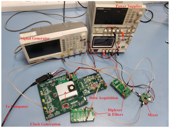
Figure 12.
Prototype system under test.
6. Test Results and Discussion
Using the single tone test method in Section 5, we obtain the frequency response of the analog front-end circuit of the synchronous mixing DBI system, as shown in Figure 13a. Using , and relative phase , we solve the perfect reconstruction equation, and the resulting reconstruction filter bank frequency response is shown in Figure 13b.
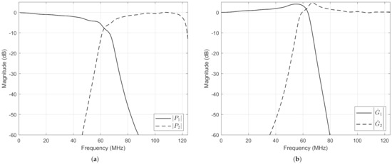
Figure 13.
Frequency response of the analysis and reconstruction filters in the synchronous mixing DBI system: (a) analysis filter bank; (b) reconstruction filter bank.
Figure 14 and Figure 15 show the spectrum of the single tone test. We choose two cases where the frequency is in the stopband of the low-pass filter in the diplexer and near the common frequency of the diplexer.
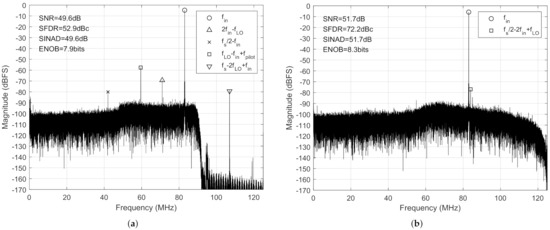
Figure 14.
Single tone test spectrum in high frequency band: (a) 83 MHz input signal for classical architecture; (b) 83 MHz input signal for synchronous mixing architecture.
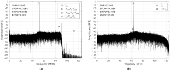
Figure 15.
Single tone test spectrum near diplexer common frequency: (a) 52 MHz input signal for classical; (b) 63 MHz input signal for synchronous mixing.
In the first case, almost all the power of the input signal enters the high frequency band of the DBI system, and the test result is shown in Figure 14. For the classical architecture, the frequency of the input signal is 83 MHz, and the power of the pilot tone is −32.5 dBm. For the synchronous mixing architecture, the frequency of the input signal is also 83 MHz. Figure 14a shows the various spurs of the classical architecture, where represents the frequency of the input signal, represents the frequency of analog LO, represents the total sampling rate of the system, and represents the frequency of the pilot tone. The largest spur in Figure 14a is caused by the intermodulation of the pilot tone and the down-conversion output of the analog mixer. The SFDR of the system is only 52.9 dBc. Some other spurs are due to the finite attenuation of the analog and digital anti-aliasing filters. For the spurs generated by other nonlinearities or digital interpolation and mixing, the maximum value is about −70 dBFS. As shown in Figure 14b, the synchronous mixing architecture does not need the pilot tone, and its SFDR is much higher than the classical one, which is 72.2 dBc. At the same time, it does not use a digital anti-aliasing filters, but synthesizes the signals from two channels by perfect reconstruction, so some other spurs are also smaller than those of the classical architecture.
In the second case, the power of single tone near the common frequency is approximately equally divided by the diplexer and then input to two channels. The test result is similar to the high frequency band, as shown in Figure 15. In Figure 15a, the largest spurious component is still produced by the intermodulation of the pilot tone and down-conversion signal. In Figure 15b, a 63 MHz signal is input into the synchronous mixing architecture. The spurs with frequency are caused by the coefficient truncation of the reconstruction filter.
Figure 16 shows the SFDR and SNR of two architectures with 5 MHz to 90 MHz single tone input signals. When the frequency of the input signal is low, the power of the signal mainly enters the low frequency channel of the DBI system. The low frequency channels of the two architectures are the same, so the SFDR is also similar. The frequency of the input signal increases, and most of the power of the signal enters the high frequency channel. It intermodulates with the pilot tone in the classical architecture, which greatly reduces the system SFDR. This problem does not exist in the synchronous mixing architecture, and when the frequency of input signal is 60 MHz to 75 MHz, the response adjustment filter attenuates spurs. Therefore, the SFDR of the synchronous mixing architecture is improved by more than 20 dB, compared with the classical one in the high frequency band. At the same time, due to the reduction of spurs, the SNR of the synchronous mixing architecture is also improved about 2–3 dB at high frequencies.
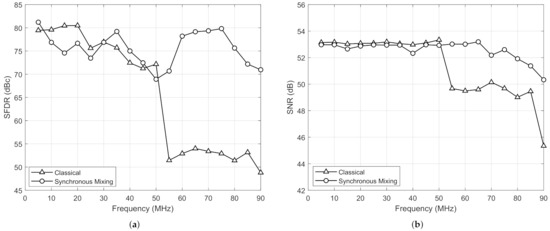
Figure 16.
SFDR and SNR of the classical and synchronous mixing architectures: (a) SFDR; (b) SNR.
Figure 17 shows the amplitude and the step response of the classical and synchronous mixing architecture. In Figure 17a, the −3 dB bandwidth of these two architectures is 90 MHz. The synchronous mixing architecture has a maximum flat response response, and is bandlimited to half of the total sampling rate, while the classical architecture is bandlimited to the frequency of LO. Due to the narrow transition band of the digital anti-aliasing filter, the amplitude response drops faster in the classical architecture. Therefore, more high frequency components of the step signal enter the synchronous mixing architecture. The step response of the two architectures is shown in Figure 17b, and the rise time is shown in Table 3. The step signal with about a 5 ns rise time is input into the two architectures, and the 200 rising edges are averaged. The rise time of synchronous mixing architecture is 0.578 ± 0.070 ns faster than the classical one.
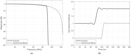
Figure 17.
Amplitude and step response of the classical and synchronous mixing architectures: (a) amplitude response; (b) step response.
Table 3.
The rise time (10–90% ) of the two architectures.
Table 4 shows the performance and cost comparison between the two architectures. During digital signal processing, the multiplication operation consumes the most computing resources. For the signal reconstruction of the above two architectures, it is mainly reflected in the order of the FIR filter and the use of DFT to solve the pilot tone phase of each sampling sequence for digital mixing. For the classical architecture, the total order of the FIR filter is 2124 (476 + 477 + 435 + 736), and this value is 1472 (736 + 736) in the synchronous mixing architecture, which is reduced by 1/3. The pilot tone in the classical architecture is 47.5 MHz, and a DFT of 10,000-point is used to analyze its phase, which can achieve a resolution of 0.025 MHz at a 250 MHz sampling rate. At the same time, an additional PLL, analog filter and power combiner are used to generate the pilot tone. These two items are not needed in the synchronous mixing architecture.
Table 4.
Comparison of performance and cost between two architectures.
Compared with the classical architecture, the only disadvantage of synchronous mixing is that it requires the bandwidth of the ADC to reach half of its sampling rate. It may not be possible for some ultra high speed ADCs, using complementary metal oxide semiconductor (CMOS) technology [33,34]. The bandwidth of the ADC only needs to reach half of the analog LO frequency under the classical architecture. In this case, we can reduce the sampling clock of the ADC to achieve synchronous mixing. As shown in Figure 17a, the signal with a higher frequency than LO cannot be sampled by the classical DBI system. However, a smaller oversampling rate will increase the overhead of the digital signal processing.
7. Conclusions
A new synchronous mixing architecture for the DBI system is proposed in this paper. Compared with the classical architecture, it does not require a pilot tone insertion system, digital interpolation filter, digital mixer, or digital anti-image filter, greatly simplifying the hardware and software structure of the DBI system. In addition, we have also built an evaluation platform with a 250 MSPS sampling rate and 14 bit resolution to test the performance of these two architectures. The test result shows that the SFDR of the new architecture improves by more than 20 dB in the high frequency band, compared with the classical architecture. The rise time of the step signal is also increased by 0.578 ± 0.070 ns with the same −3 dB bandwidth. In addition, the total order of the FIR filter is reduced by 1/3, and the 10,000-point DFT calculation for the pilot tone phase analysis is removed during reconstruction of each sampling sequence. In general, the new architecture has advantages over the classical one in term of the implementation cost and performance.
Author Contributions
Conceptualization, X.J. and J.W.; methodology, X.J.; software, Y.M.; validation, X.J. and Y.M.; formal analysis, X.J.; investigation, X.J.; resources, J.W.; data curation, X.J. and Y.M.; writing—original draft preparation, X.J.; writing—review and editing, J.W.; visualization, Y.M.; supervision, J.W.; project administration, J.W.; funding acquisition, J.W. All authors have read and agreed to the published version of the manuscript.
Funding
This research was funded by the Strategic Priority Research Program of the Chinese Academy of Sciences (Grant No. XDC07020403), and the Major National Science and Technology Special Program of China (Grant No. 2017ZX05008-008-041).
Data Availability Statement
The data presented in this study are available on request from the corresponding author.
Conflicts of Interest
The authors declare no conflict of interest.
References
- Cruz, P.; Carvalho, N.B.; Remley, K.A. Designing and testing software-defined radios. IEEE Microw. Mag. 2010, 11, 83–94. [Google Scholar] [CrossRef]
- Raybon, G.; Guan, B.; Adamiecki, A.; Winzer, P.J.; Fontaine, N.; Chen, S.; Pupalaikis, P.J.; Delbue, R.; Doshi, K.; Bhat, B.; et al. 160-Gbaud coherent receiver based on 100-GHz bandwidth, 240-GS/s analog-to-digital conversion. In Proceedings of the 2015 Optical Fiber Communications Conference and Exhibition (OFC), Optical Society of America, Los Angeles, CA, USA, 22–26 March 2015; pp. 1–3. [Google Scholar]
- Pupalaikis, P.J.; Yamrone, B.; Delbue, R.; Khanna, A.S.; Doshi, K.; Bhat, B.; Sureka, A. Technologies for very high bandwidth real-time oscilloscopes. In Proceedings of the 2014 IEEE Bipolar/BiCMOS Circuits and Technology Meeting (BCTM), Coronado, CA, USA, 28 September–1 October 2014; pp. 128–135. [Google Scholar]
- Ding, H.; Wu, D.; Zheng, X.; Zhou, L.; Chen, T.; Lv, F.; Wang, J.; An, B.; Wu, J.; Liu, X. A Low-Distortion 20 GS/s Four-Channel Time-Interleaved Sample-and-Hold Amplifier in 0.18 μm SiGe BiCMOS. Electronics 2020, 9, 20. [Google Scholar] [CrossRef] [Green Version]
- Jia, H.; Guo, X.; Zheng, X.; Xu, X.; Wu, D.; Zhou, L.; Wu, J.; Liu, X. A 4-bit 36 GS/s ADC with 18 GHz Analog Bandwidth in 40 nm CMOS Process. Electronics 2020, 9, 1733. [Google Scholar] [CrossRef]
- Black, W.C.; Hodges, D.A. Time interleaved converter arrays. IEEE J. Solid State Circuits 1980, 15, 1022–1029. [Google Scholar] [CrossRef]
- Seo, M.; Rodwell, M.J.; Madhow, U. Comprehensive digital correction of mismatch errors for a 400-Msamples/s 80-dB SFDR time-interleaved analog-to-digital converter. IEEE Trans. Microw. Theory Tech. 2005, 53, 1072–1082. [Google Scholar]
- Li, J.; Pan, J.; Zhang, Y. Automatic calibration method of channel mismatches for wideband TI-ADC system. Electronics 2019, 8, 56. [Google Scholar] [CrossRef] [Green Version]
- Kurosawa, N.; Kobayashi, H.; Maruyama, K.; Sugawara, H.; Kobayashi, K. Explicit analysis of channel mismatch effects in time-interleaved ADC systems. IEEE Trans. Circuits Syst. I Fundam. Theory Appl. 2001, 48, 261–271. [Google Scholar] [CrossRef] [Green Version]
- El-Chammas, M.; Murmann, B. General analysis on the impact of phase-skew in time-interleaved ADCs. IEEE Trans. Circuits Syst. I Regul. Pap. 2009, 56, 902–910. [Google Scholar] [CrossRef]
- Razavi, B. Design considerations for interleaved ADCs. IEEE J. Solid State Circuits 2013, 48, 1806–1817. [Google Scholar] [CrossRef] [Green Version]
- Velazquez, S.R.; Nguyen, T.Q.; Broadstone, S.R. Design of hybrid filter banks for analog/digital conversion. IEEE Trans. Signal Process. 1998, 46, 956–967. [Google Scholar] [CrossRef] [Green Version]
- Mazlouman, S.J.; Mirabbasi, S. A frequency-translating hybrid architecture for wide-band analog-to-digital converters. IEEE Trans. Circuits Syst. II Express Briefs 2007, 54, 576–580. [Google Scholar] [CrossRef]
- Pupalaikis, P.J. An 18 GHz bandwidth, 60 GS/s sample rate real-time waveform digitizing system. In Proceedings of the 2007 IEEE/MTT-S International Microwave Symposium, Honolulu, HI, USA, 3–8 June 2007; pp. 195–198. [Google Scholar]
- Mazlouman, S.J.; Sheikhaei, S.; Mirabbasi, S. Digital compensation techniques for frequency-translating hybrid analog-to-digital converters. IEEE Trans. Instrum. Meas. 2010, 60, 758–767. [Google Scholar] [CrossRef]
- Pupalaikis, P.J.; Schnecker, M. A 30 GHz bandwidth, 80 GS/s sample rate real-time waveform digitizing system. In Proceedings of the National Fiber Optic Engineers Conference, Optical Society of America, San Diego, CA, USA, 21–25 March 2010; pp. 1–3. [Google Scholar]
- Knierim, D. Ultra-wide-bandwidth oscilloscope architectures and circuits. In Proceedings of the 2014 IEEE Bipolar/BiCMOS Circuits and Technology Meeting (BCTM), Coronado, CA, USA, 28 September–1 October 2014; pp. 136–142. [Google Scholar]
- Song, J.; Tian, S.; Hu, Y.H. Analysis and correction of combined channel mismatch effects in frequency-interleaved ADCs. IEEE Trans. Circuits Syst. I Regul. Pap. 2018, 66, 655–668. [Google Scholar] [CrossRef]
- Zhao, Y.; Ye, P.; Meng, J.; Yang, K.; Gao, J.; Pan, Z.; Huang, W.; Song, J.; Dai, X. Compensation Module Design for Overlapping Band in Band-Interleaved Data Acquisition Systems Based on Hybrid Particle Swarm Optimization Algorithm. IEEE Access 2020, 8, 178835–178848. [Google Scholar] [CrossRef]
- Zhao, Y.; Ye, P.; Yang, K.; Meng, J.; Lei, M. A field programmable gate array based synchronization mechanism of analog and digital local oscillators in bandwidth-interleaved data acquisition systems. Rev. Sci. Instrum. 2021, 92, 034703. [Google Scholar] [CrossRef]
- Pupalaikis, P.J. The Interleaving Process in Digital Bandwidth Interleaving Scopes. Available online: http://cdn.teledynelecroy.com/files/whitepapers/interleaving_process_in_dbi_scopes.pdf (accessed on 17 April 2021).
- Asemani, D.; Oksman, J.; Duhamel, P. Subband architecture for hybrid filter bank A/D converters. IEEE J. Sel. Top. Signal Process. 2008, 2, 191–201. [Google Scholar] [CrossRef] [Green Version]
- Oppenheim, A.V.; Schafer, R.W.; Buck, J.R. Discrete-Time Signal Processing, 2nd ed.; Prentice Hall: Upper Saddle River, NJ, USA, 1999; pp. 166–173. [Google Scholar]
- Rabiner, L.R.; McClellan, J.H.; Parks, T.W. FIR digital filter design techniques using weighted Chebyshev approximation. Proc. IEEE 1975, 63, 595–610. [Google Scholar] [CrossRef]
- XILINX. UltraScale Architecture and Product Data Sheet: Overview. Available online: https://www.xilinx.com/support/documentation/data_sheets/ds890-ultrascale-overview.pdf (accessed on 29 April 2021).
- Razavi, B. RF Microelectronics, 2nd ed.; Prentice Hall: Upper Saddle River, NJ, USA, 2012; pp. 14–21. [Google Scholar]
- Magalhães, J.P.; Vieira, J.M.; Gómez-Garcia, R.; Carvalho, N.B. Bio-inspired hybrid filter bank for software-defined radio receivers. IEEE Trans. Microw. Theory Tech. 2013, 61, 1455–1466. [Google Scholar] [CrossRef]
- Matthaei, G.; Cristal, E. Theory and design of diplexers and multiplexers. Adv. Microw. 2013, 2, 237–324. [Google Scholar]
- Pupalaikis, P.J.; Graef, D.C. High Bandwidth Oscilloscope. U.S. Patent 10,333,540, 25 June 2019. [Google Scholar]
- Kester, W.; Engineeri, A.D.I. Data Conversion Handbook; Newnes: Boston, FL, USA, 2005; pp. 403–410. [Google Scholar]
- Eskeldson, D.; Kellum, R.; Whiteman, D. A Digitizing Oscilloscope Time Base and Trigger System Optimized for Throughput and Low Jitter. Hewlett-Packard J. 1993, 44, 24–30. [Google Scholar]
- KeysightTechnologies. Understanding Oscilloscope Frequency Response and Its Effect on Rise-Time Accuracy. Available online: https://www.keysight.com/cn/zh/assets/7018-01129/application-notes/5988-8008.pdf (accessed on 19 June 2021).
- Kull, L.; Toifl, T.; Schmatz, M.; Francese, P.A.; Menolfi, C.; Braendli, M.; Kossel, M.; Morf, T.; Andersen, T.M.; Leblebici, Y. 22.1 a 90 gs/s 8b 667 mw 64× interleaved sar adc in 32 nm digital soi cmos. In Proceedings of the 2014 IEEE International Solid-State Circuits Conference Digest of Technical Papers (ISSCC), San Francisco, CA, USA, 9–13 February 2014; pp. 378–379. [Google Scholar]
- Cao, J.; Cui, D.; Nazemi, A.; He, T.; Li, G.; Catli, B.; Khanpour, M.; Hu, K.; Ali, T.; Zhang, H.; et al. 29.2 A transmitter and receiver for 100 Gb/s coherent networks with integrated 4× 64 GS/s 8b ADCs and DACs in 20 nm CMOS. In Proceedings of the 2017 IEEE International Solid-State Circuits Conference (ISSCC), San Francisco, CA, USA, 5–9 February 2017; pp. 484–485. [Google Scholar]
Publisher’s Note: MDPI stays neutral with regard to jurisdictional claims in published maps and institutional affiliations. |
© 2021 by the authors. Licensee MDPI, Basel, Switzerland. This article is an open access article distributed under the terms and conditions of the Creative Commons Attribution (CC BY) license (https://creativecommons.org/licenses/by/4.0/).