1. Introduction
Intensive research has been conducted on ultraviolet (UV) photodetectors (PDs) to expand their applications to fields, including the military (e.g., in hazard detection), manufacture factory (e.g., for maintaining safety), and medical fields. UV radiation can cause skin cancer, skin aging, eye damage, and weakening of the immune system. The health of people who work outdoors and are exposed to solar UV radiation and those engaged in occupations that involve UV radiation exposure from non-solar sources (e.g., in arc welding, curing of paints and inks, and the disinfection of equipment in hospitals and laboratories) could be adversely affected. To minimize the risk and damage from UV exposure in work and daily life activities, direct and spontaneous UV detection is necessary.
Recently, flexible devices have become important components for internet of things (IoTs) because their unlimited form factor facilitates spontaneous device communication with the desired signal. Organic semiconductors have attracted substantial attention, particularly for fabricating flexible PDs, because they can be used to produce lightweight films with a free form factor over various large-area substrates by using a simple, inexpensive, and low-temperature process [
1,
2,
3,
4,
5,
6,
7]. High-sensitivity organic PDs have recently attracted considerable attention for aerospace, civil, biological, environmental, and military applications [
8,
9]. However, improvement in device performance is difficult in the case of organic PDs that are prepared using organic active materials only (e.g., charge carrier mobility, uniformity, durability in air, and defects in the organic crystal structure). Nowadays, hybrid devices with both organic and inorganic materials are receiving considerable attention because of their superior performance [
10,
11,
12]. These devices offer many advantages over both all-inorganic devices and all-organic devices, such as wideband absorption, high carrier mobility, and outstanding electrical performance.
However, substantial challenges exist in producing the final hybrid devices. First, the poor interface of hybrid device tends to increase a leakage current, resulting in high power consumption. In particular, the interface between the active layers and electrodes in these devices, which both injects and extracts charge, strongly affects their leakage current. Thus, interface of hybrid device should be carefully designed by controlling the work function and surface energy [
13,
14]. In addition, since morphological defects on the surface of the active layer during the spin-casting process can cause an electrical short-circuit between the anode and cathode, their number should be reduced [
15]. Second, a final PD capable of realizing spontaneous communication will require several components such as energy generator, a signal receiver, and display. The fabrication of a flexible integrated circuit with all three devices is extremely challenging, and this circuit has many disadvantages, such as heat generation, safety concerns, and a high weight, limiting the usage of flexible PDs. Therefore, a new strategy is needed to develop a high-performance PD for spontaneous communication.
In this study, we designed simple, reproducible, and air-stable solution-processed hybrid organic PD devices on flexible substrates. These devices consist of a very thin ferroelectric copolymer interlayer between the optical active layer and cathode. The proposed structure of the devices enhanced their charge-transfer performance via ferroelectric-poling interface layer. The ferroelectric copolymer layer not only controlled the optical charge transfer, but also improved durability under bending stress conditions. In addition, the ferroelectric copolymer displayed a memory effect, resulting in a spontaneous input-to-output signal display.
2. Materials and Methods
Fabrication of hybrid PD: Indium tin oxide (ITO)-coated (coating thickness: 130 nm) polyethylene terephthalate (PET) substrate (304.8 mm × 304.8 mm × 5 mm, ITO/PET) was first cleaned in ultrasonic bath of isopropyl alcohol and acetone. The substrate was then dried on a hot plate at 100 °C for 30 min. This was followed by UV/ozone treatment for 10 min to clean and remove any organic residues present on the surface. Then, the substrate was spin-coated with a poly(3,4-ethylenedioxythio-phene):poly(styrenesulfonate) (PEDOT:PSS) aqueous solution with a rotation speed of 3000 rpm, yielding a 70-nm-thick thin film on top of the substrates.
Poly(9-vinylcarbazole) (PVK; Sigma–Aldrich) and zinc oxide (ZnO) nanoparticles were used to prepare the photoactive heterojunction layer in the hybrid organic PDs. The photoactive layers were prepared by the sequential deposition of ZnO nanoparticles and PVK solution. For the photoactive film, a PVK solution (22.5 mg PVK per millilitre of chlorobenzene) was spin-cast onto the PEDOT:PSS-coated ITO/PET substrate at 1500 rpm for 30 s. Next, the substrates were spin-coated with the prepared ZnO nanoparticle solution (7 wt%) at 1500 rpm for 60 s. The films were annealed at 80 °C for 30 min and then 120 °C for 30 min. The thermal annealing was conducted on a hot plate under ambient air conditions. A very thin organic copolymer layer consisting of poly(vinylidene fluoride-co-trifluoroethylene (PVDF-TrFE; 70:30 mol%, 1 wt% in cyclohexanone, PiezoTech) was formed on the photoactive films by spin-coating at 3000 rpm for 30 s followed by drying at 120 °C for 12 h to increase the number of crystallites. Finally, an electron-collection electrode composed of Al (thinkness~100 nm) was deposited onto the prepared films using electron beam evaporation through a shadow mask at a pressure of ~5 × 10
−6 Torr. Thus, the hybrid PD was obtained.
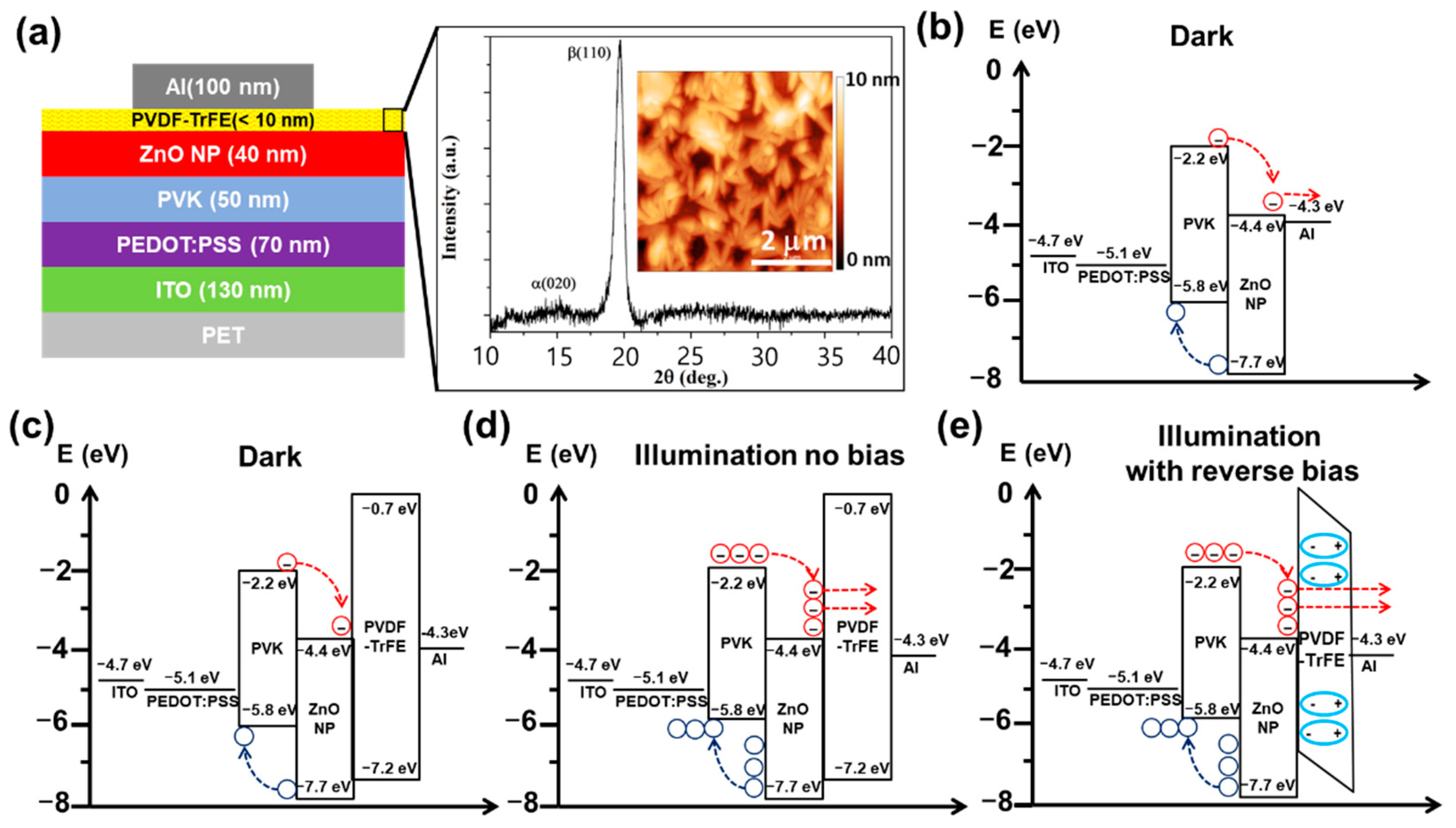
Figure 1a shows the sandwich configuration of the resultant PD with the PEDOT:PSS hole transport layer (~70-nm-thick), the PVK (~50 nm) and ZnO nanoparticle (~40 nm) layer as the hybrid photoactive layer, and the PVDF-TrFE ferroelectric layer (~10-nm-thick) on the ITO/PET substrate.
Fabrication of UV light-responsive memory devices: To fabricate UV-light-responsive memory devices, we separately fabricated the top and bottom layers as follows: For the top layer, a Nylon 6 alignment layer was deposited onto the ITO/PET substrate by spin coating, and then, the alignment layer was rubbed to flatten the surface. Then, the top of the Nylon 6 layer was coated with a spacer to create some space to inject the liquid crystals. The bottom layer was attached with the treated top layer through glue at the edge of the substrate. The hybrid-PD was fabricated using the abovementioned method and used for the bottom layer. Then, the liquid crystals were injected between the top layer and hybrid-PD bottom layer.
Characterization: Atomic force microscopy (AFM; Dimension 3100) images in the tapping mode were obtained using a Nanoscope IIIa controller. The electrical characteristics of the PDs were measured in air using an Agilent 4156C Precision Semiconductor Parameter Analyzer. Calibration of the UV light-emitting diode source was performed using a power meter (OAI 306).
3. Results and Discussion
The basic working principle of an organic PD is that carriers are generated under illumination at a selected wavelength (~365 nm), and the holes and electrons are collected at the anode and cathode, respectively. The optical sensitivity is determined by the interaction between the organic active layer and exposed light source with an applied external bias [
16,
17,
18]. Low dark (leakage) currents at negative bias play a key role and determine important properties of PDs, such as the detectivity, signal-to-noise ratio, external quantum efficiency (EQE), and responsivity (R). Thus, the dark current should be reduced by controlling the interface of devices. Electron/hole transfer or the insertion of a blocking layer between the active layer and electrode is the most common method to control the interface in organic optoelectronic devices [
19,
20,
21]. The ZnO nanoparticles/PVK layer in the PD prepared in this study mimicked the n-p heterojunction structure, thereby enhancing the responsivity of devices by rectifying the Schottky contact in the dark (
Figure 1b). Holes were transported to PVK while the electrons were trapped in the ZnO nanoparticles due to a strong quantum confinement effect in the nanoparticles [
22,
23]. The right side of
Figure 1a shows the X-ray diffraction (XRD) pattern of the PVDF-TrFE ferroelectric copolymer film. The sharp XRD peak at 19.8° corresponds to the highly 110-oriented (β-phase) copolymer thin film, which resulted in a strong ferroelectric response and increased crystallinity [
24]. The AFM image (
Figure 1a, inset) also matched with the XRD analysis results. The topography depicted acicular crystalline grains with approximate lengths of 1 μm and widths of 100 nm, and its mean roughness was 1.98 nm. The ferroelectric response behaviour of PVDF-TrFE was useful for the following: (1) reducing the leakage current by modulating the band alignment with the external electric field and (2) exhibiting a short memory effect for spontaneous communication. PVDF-TrFE is a ferroelectric material that exhibits remnant polarization without the application of an external electric field because of spontaneous polarization, which can be reversed by an externally applied voltage that is larger than the coercive field [
25,
26]. PVDF-TrFE thus exhibits nonlinear properties that depend on the intensity of the external electric field. Ferroelectricity leads to the movement of dipoles in the crystalline structure, which is identified as spontaneous polarization and the dipole of ferroelectric molecules is aligned by the electric field. The polarization of the dipoles modulated the Schottky barrier between ZnO and the Al electrode.
The operation principle of our devices is explained by the energy band diagrams presented in
Figure 1c–e. Under dark conditions, the electron injection is impeded by the low electron mobility of PVK and large electron injection barrier of the PVDF-TrFE, high-k (~10.5) dielectric layer [
27]. Further, the hole-trap-derived electron injection between the active layer and ferroelectric layer is severely constrained due to increased Schottky barrier between ZnO and the Al electrode (
Figure 1c). Furthermore, electron transport was hampered with the negative external bias because of the polarization of the ferroelectric layer, so numerous electrons were trapped at the interface between ZnO nanoparticle layer and PVDF-TrFE. Therefore, a low dark current can be produced and maintained.
However, under illumination, the PVK/ZnO nanoparticle layer absorbs the incident UV light and generates numerous free electron–hole pairs via the internal photoelectric effect (
Figure 1d). The photo-excited electrons and holes increase the electrical conductivity of the device and move in opposite directions, with the holes flowing toward the ITO electrode and the electrons flowing toward the Al electrode. With the forward bias, electrons easily move toward the Al electrode through a direct tunnelling effect. Even when the reverse bias is applied, numerous electrons are rapidly transported via the direct tunnelling effect, and this effectively prevents the flow of leakage current under dark conditions because the polarization of the ferroelectric layer is maintained with the reverse external bias (
Figure 1e). Thus, our designed devices can be used as a UV photodetector with low dark current under the reverse bias.
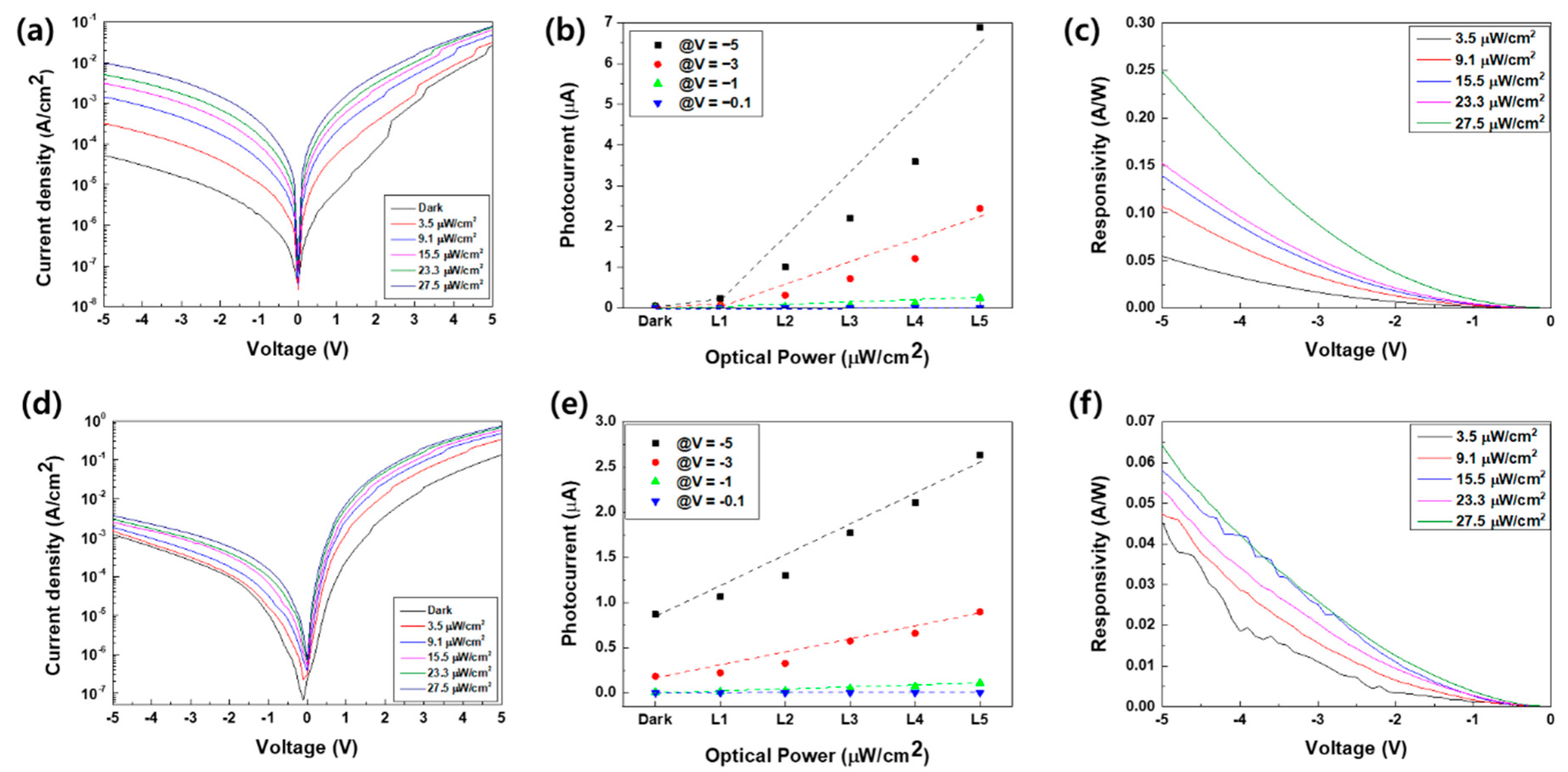
To evaluate the optoelectronic performance of the hybrid PD with and without the ferroelectric layer, we measured the current–voltage (I–V) characteristics both with and without the ferroelectric layer under different incident UV light intensity (365 nm wavelength), and the results are presented in
Figure 2a,d, respectively. The plots were obtained from the mean of five measurements with a standard deviation of 5%. The devices were operated in the photoconductive mode by gradually increasing the incident light intensity. As the power increased, the photocurrent also increased because of the addition of the internal photocurrent to the external diode current of the applied electric field. In particular, the dark current levels differed noticeably between the devices with and without the ferroelectric layer.
Figure 2b,e show the correlation between the photocurrent of each device and the illumination power, as derived from
Figure 2a,d. The photocurrent first linearly increased with the light intensity. In other words, the slope indicates the responsivity of the devices, and the output current level can be predicted from the slope. The output current in the dark conditions for the device without the ferroelectric layer was much higher than that for the device with the ferroelectric layer. This is because the small Schottky barrier between ZnO and Al facilitates electron transport.
The responsivity was extracted from the I–V plots of the devices (
Figure 2c,f). The maximal responsivity (R = |I
Light − I
Dark|/P
Light) was 250 and 64 mA/W for the device with and without the ferroelectric layer, respectively, when an external bias of −5 V and UV light intensity of 27.5 μW/cm
2 were applied onto an effective area of the cathode (diameter of Al electrode = 300 μm). A simple comparison of our results with those of previous studies on UV PDs with the PVK–ZnO nanoparticle heterojunction is difficult. Lee et al. recently reported a responsivity of 85.8 mA/W at −5 V bias with 1 mW/cm
2 UV light intensity for ZnO/PVK PD device on a glass substrate [
28]. Even though these researchers used an incident light intensity that was approximately 36 times higher than that used for our measurement, the responsivity of our device was three times higher. Moreover, we calculated the external quantum efficiency (EQE = 1240 × R
λ/λ) based on the curves of responsivity versus voltage (R–V curves). Values of ~84.9% and ~21.7% were obtained for the devices with and without the ferroelectric layer, respectively, for an incident light wavelength of 365 nm. Previously reported values of the EQE for Si-based PDs range between 50% and 90%. This value is affected by the wavelength of the incident light and type of photodiode. We believed that the proposed device structure with the ferroelectric layer interface improves both the responsivity and EQE by approximately four times compared with those without the copolymer layer. Moreover, we measured responsivity of the hybrid PD with PVDF-TrFE under forward bias. Unlike the same device under reverse bias, responsivity decreased as UV light power increased because the different direction of polarization facilitated temporal hole transport toward PVDF-TrFE. Thus, our device demonstrated better performance with the reverse bias.
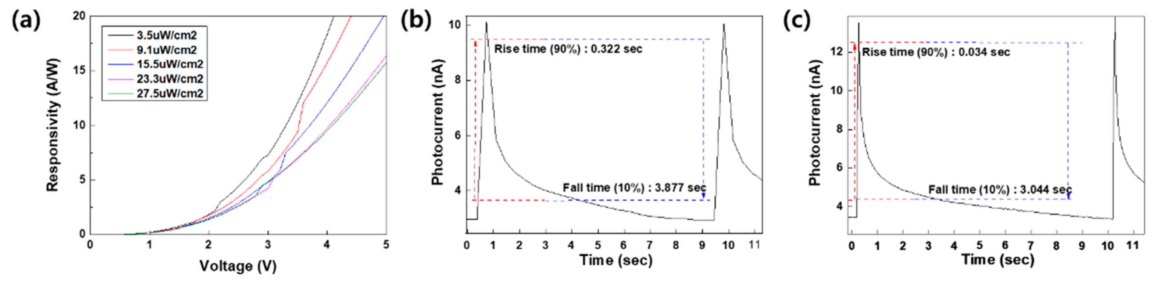
In addition to the responsivity, the ferroelectric layer improved the photoresponse time, as shown in
Figure 3b,c. The response time was determined using a 1% pulse wave of 0.1-Hz frequency and a light intensity of 15.5 μW/cm
2 provided by a 365-nm-wavelength UV source under an external bias of −1 V. The rise and fall times were defined as the times required to reach from 10% to 90% and from 90% to 10% of photocurrent in the light on/off state, respectively. Rise times of 0.034 and 0.322 s and fall times of 3.044 and 3.877 s were determined for the devices with and without the ferroelectric layer, respectively. The decline of the photocurrent for both devices had two different slopes: Exponential decay was calculated from the bi-exponential fit (
Table 1). The first decay (half-life (
τ1) and fraction (
f1)) is attributed to the simultaneous carrier flow and the second decay (half-life (
τ2) and fraction (
f2)) is attributed to slow nonlinear decline resulting from the large electron traps owing to the non-uniform layer of stacked ZnO nanoparticles [
29]. The
τ1 (
f1) values of the hybrid PD devices without and with PVDF-TrFE were 0.23 s (0.53) and 0.15 s (0.85), respectively. This indicates that the hybrid PD with the ferroelectric layer facilitates carrier separation. Consequently, the ferroelectric layer enhanced the charge transfer rate by approximately 10 times, and the rise time was more than two times shorter than that reported in a recent study. We believe that device performance using the PVDF-TrFE layer enhanced due to two factors: chemical cause and polarization of the ferroelectric layer. Heat treatment for 12 h after PVDF-TrFE coating reduced chemical residual in the ZnO nanoparticle layer and the improved interface between PVDF-TrFE layer, resulting in faster responsivity. Even though the ferroelectric layer was ultra-thin, it functioned as a dielectric material, and the spontaneous polarization of the ferroelectric layer contributed to accumulation of charge from the continuous external bias. Thus, we consider that the polarized ferroelectric layer facilitates carrier accumulation at the interface between ZnO nanoparticles and ferroelectric materials, rather than inducing charge accumulation at the deep-level traps of ZnO nanoparticles, resulting in a fast response time with the ferroelectric layer.
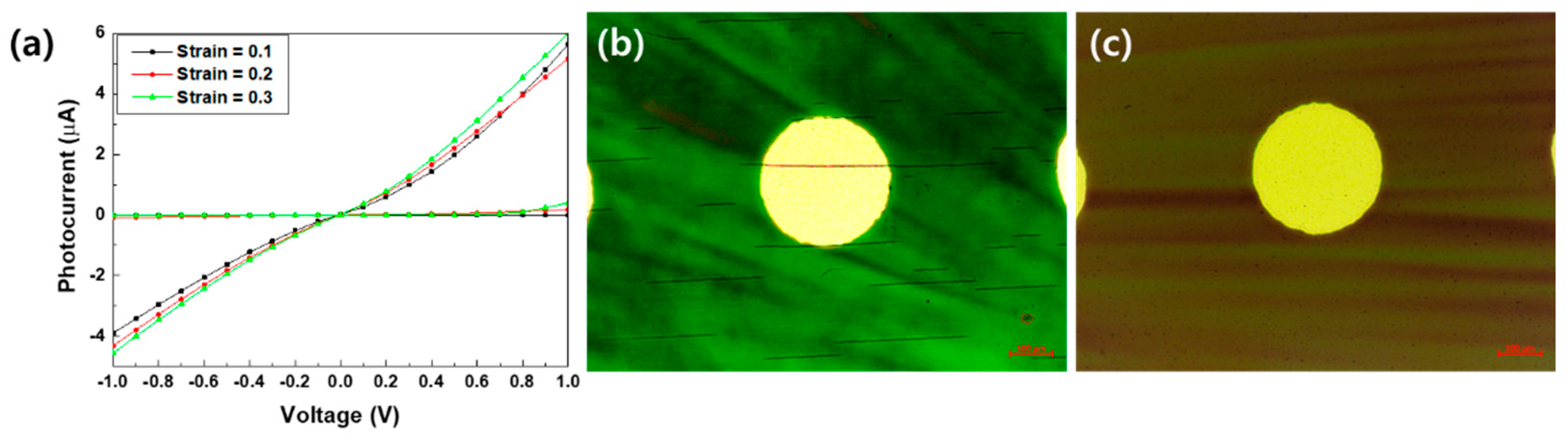
We also tested the durability of our devices by subjecting them to tensile stress in the bending test in ambient air. The photo/dark currents for various strains are shown in
Figure 4a. The PD with the photoelectric layer exhibited stable photocurrent under a maximum tensile strain of 0.3 in the bending state. However, the PD without the ferroelectric layer exhibited a short-circuit phenomenon over 0.1 strain (not shown). This result occurred because a sub-microscale crack was formed on the deposited ITO electrode on the PET substrate under bending stress in the device without the copolymer layer. The optical microscopy image in
Figure 4b shows the cracks generated in the device without the ferroelectric layer both on the top electrode and in the photoactive layer after the bending stress was applied. However, as shown in
Figure 4c, no crack damage is visible for the device with the ferroelectric layer for a strain of 0.3 under 100 bending cycles. Therefore, the mechanical properties can be improved with the introduction of the copolymer buffer layer.
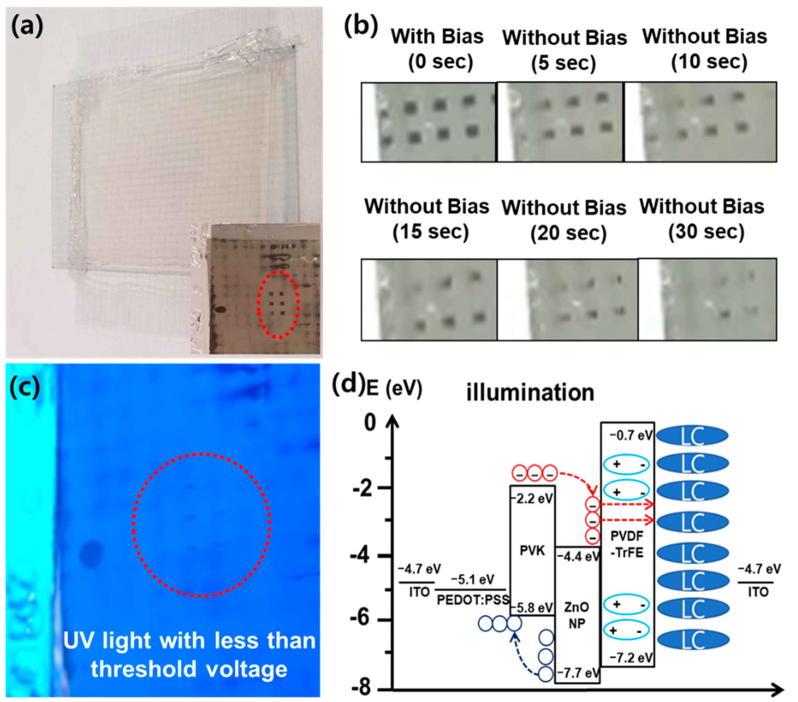
Finally, UV light-responsive memory devices were fabricated with 5 wt% of the ferroelectric layer.
Figure 5a shows the microscopy image of produced UV light-responsive memory devices. Without any bias, the device exhibited a white colour due to transparent nature of the liquid crystals with in-plane field alignment. However, when the threshold voltage (~9 V) was applied, the liquid crystals rotated, resulting in a vertical field alignment, and turned black, as shown in the inset of
Figure 5a. The memory effect of ferroelectric materials was examined, and the on-state of UV light-responsive memory devices was maintained for 30 s (
Figure 5b). Moreover, the device turned on upon UV exposure under 3 V (
Figure 5c). In the UV light-responsive memory devices, the applied bias voltage was less than the threshold voltage. Under dark conditions, an electric field was incapable of rotating the liquid crystals, resulting in the device with the white colour. However, upon UV light irradiation with the same bias voltage (
Figure 5d), the photocurrent was generated, and numerous electrons were transported toward liquid crystals via the direct tunnelling effect. The additional carriers helped to rotate the liquid crystals, resulting in the black colour of the device, even under a bias voltage less than the threshold voltage.


