Article

An 87% Power-Efficiency Hybrid of Voltage- and Current-Mode Line Driver with an Adaptive Amplitude Tuning

1
The School of Electrical Engineering, Korea Advanced Institute of Science and Technology, Daejeon 34141, Korea
2
The School of Electrical and Computer Science, Gwangju Institute of Science and Technology, Gwangju 61005, Korea
*
Author to whom correspondence should be addressed.
Electronics 2021, 10(15), 1785; https://doi.org/10.3390/electronics10151785
Submission received: 25 June 2021 / Revised: 13 July 2021 / Accepted: 18 July 2021 / Published: 26 July 2021
(This article belongs to the Section Circuit and Signal Processing)

Abstract

:
This brief presents a hybrid of voltage- and current-mode line drivers for the turbo controller area network (CAN). The current-mode scheme prevents signal attenuation caused by source termination resistors, and it enhances signal power efficiency. On top of that, an adaptive amplitude tuning is implemented to mitigate non-linearity and closed-loop gain variations against load impedance variations. The proposed line driver achieves 87.0% power-efficiency and total harmonic distortion, plus noise (THD+N) of −49.0 dB at an input frequency of 40 MHz and output swing of 2.8 VPP differential. The adaptive amplitude tuning allows load impedance variations from 80 Ω to 160 Ω. The total power consumption is 37.6 mW with a 1.8 V supply voltage in 180 nm CMOS, and it occupies 0.377 mm2.

1. Introduction

Line drivers (LDs) have been widely used in various wire-lined channels, such as integrated service digital network (IDSN) transceivers, digital subscriber line (DSL), and cable modems [1]. The LD acts as an analog buffer, which transmits sufficient output current to drive the low-load impedances. The LD’s significant design aspects are high output swing, low distortion, high signal power efficiency (ηpower), and appropriate impedance matchings for line impedance variations over process variations [1]. Voltage-mode line drivers (VMLDs) [2,3,4], Ref. [5] have been widely used due to their excellent linearity and power consumption since they source fewer currents to the load than current-mode line drivers (CMLDs) [6]. A fully differential difference VMLD with a dual common-mode feedback (CMFB) circuit [7] allows a faster transient response, which results in an improved linearity. Another VMLD assisted with an active termination circuit and dynamic power supply control circuit [3] allows enhanced power efficiency. However, the series source termination in the VMLDs attenuates the total signal power delivered to the channel lines [8], as shown in Figure 1. In addition, the VMLD topologies typically require a 1-to-N transformer to increase its signal swings on the channel lines. Therefore, the VMLD architecture features low ηpower and typically requires extra passive components.
On the other hand, CMLDs [8,9,10] consist of parallel source termination, and the signal does not suffer from matching attenuation, which leads to higher ηpower. The higher signal swing also guarantees improved robustness against external noise and electromagnetic interference (EMI). The output stage of a current-mode H-bridge cascode, assisted with local auxiliary loops [8], enhances mirroring accuracy to alleviate the signal linearity. However, it requires additional circuits and power consumption for the auxiliary amplifiers, and the cascode topology reduces the allowable output signal swings. Current-mirroring topologies with an adaptive termination tuning [1,5,9] mitigate closed-loop variations and unmatched termination against the transmission line variations. However, the tuning technique reduces the output signal swing due to the small series resistance between the supply and the output nodes.
This paper presents a hybrid of closed-loop voltage-mode using an operational amplifier (OPAMP) and open-loop current-mode class-AB current replica cells with a digital-based adaptive amplitude tuning (AAT). The AAT controls the current replica cells’ sizes to prevent the closed-loop voltage gain and the signal linearity variations against the load impedance variations in a range of 80 Ω to 160 Ω with a 32-bit tuning step. The tuning circuit reduces the two variations without degrading the ηpower and the output signal swings. The proposed hybrid of a VMLD and CMLD achieves total harmonic distortion plus noise (THD+N) of −49.0 dB at an input frequency of 40 MHz and an output swing of 2.8 VPP differential. The proposed LD is designed for a turbo controller area network (CAN) [11] for in-vehicle networks, as shown in Figure 2. The turbo CAN process modulates analog data rather than binary signals to boost the data transmission speed from 10 Mbps to over 100 Mbps. Each end of the bus lines is terminated with 120 Ω.
This paper is organized as follows. Section 2 introduces the architecture and analysis of the proposed LD. Section 3 describes the analysis of the proposed AAT. Section 4 delivers the measurement results of the driver, and Section 5 draws the conclusions.

2. Proposed Hybrid of Voltage- and Current-Mode Line Driver

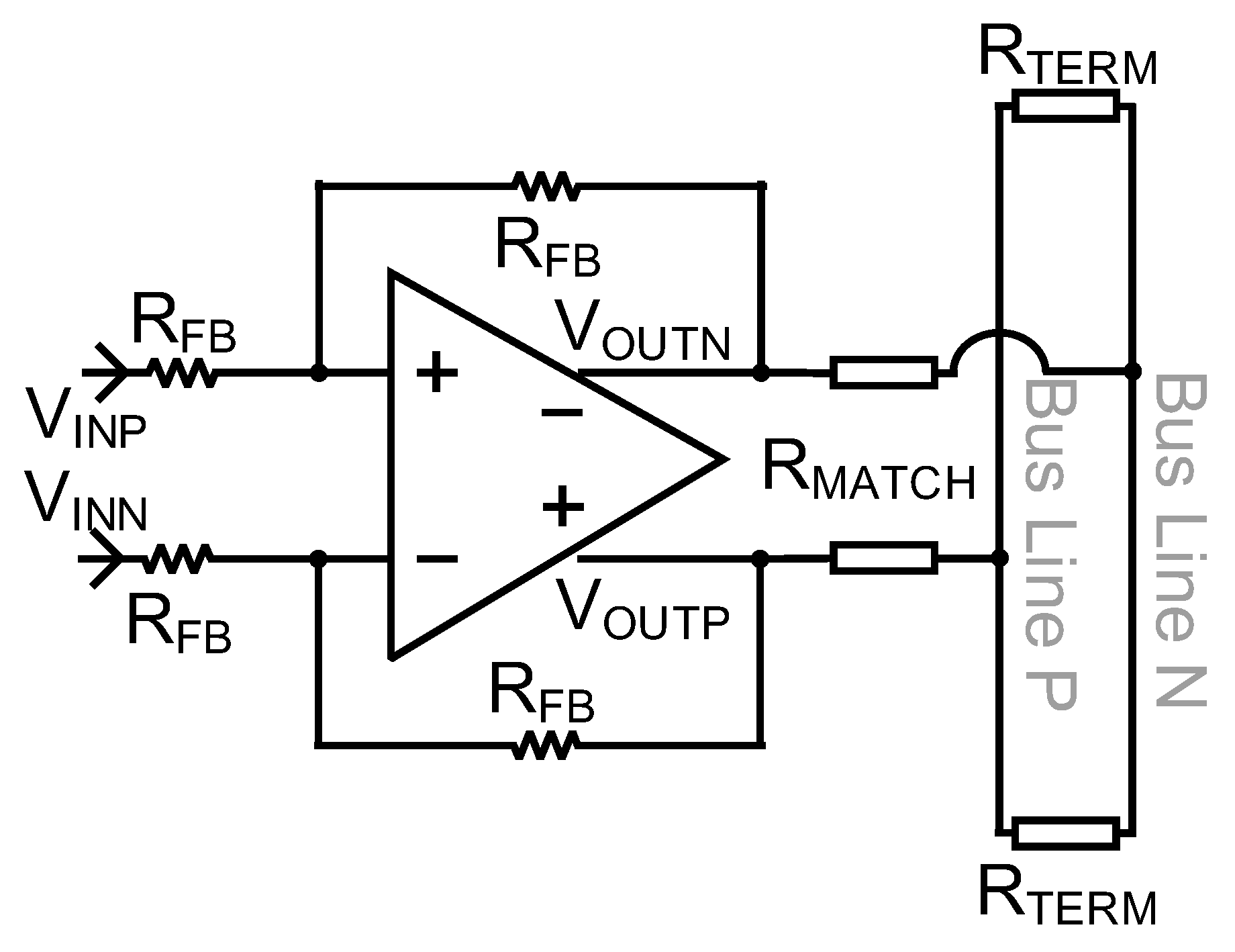
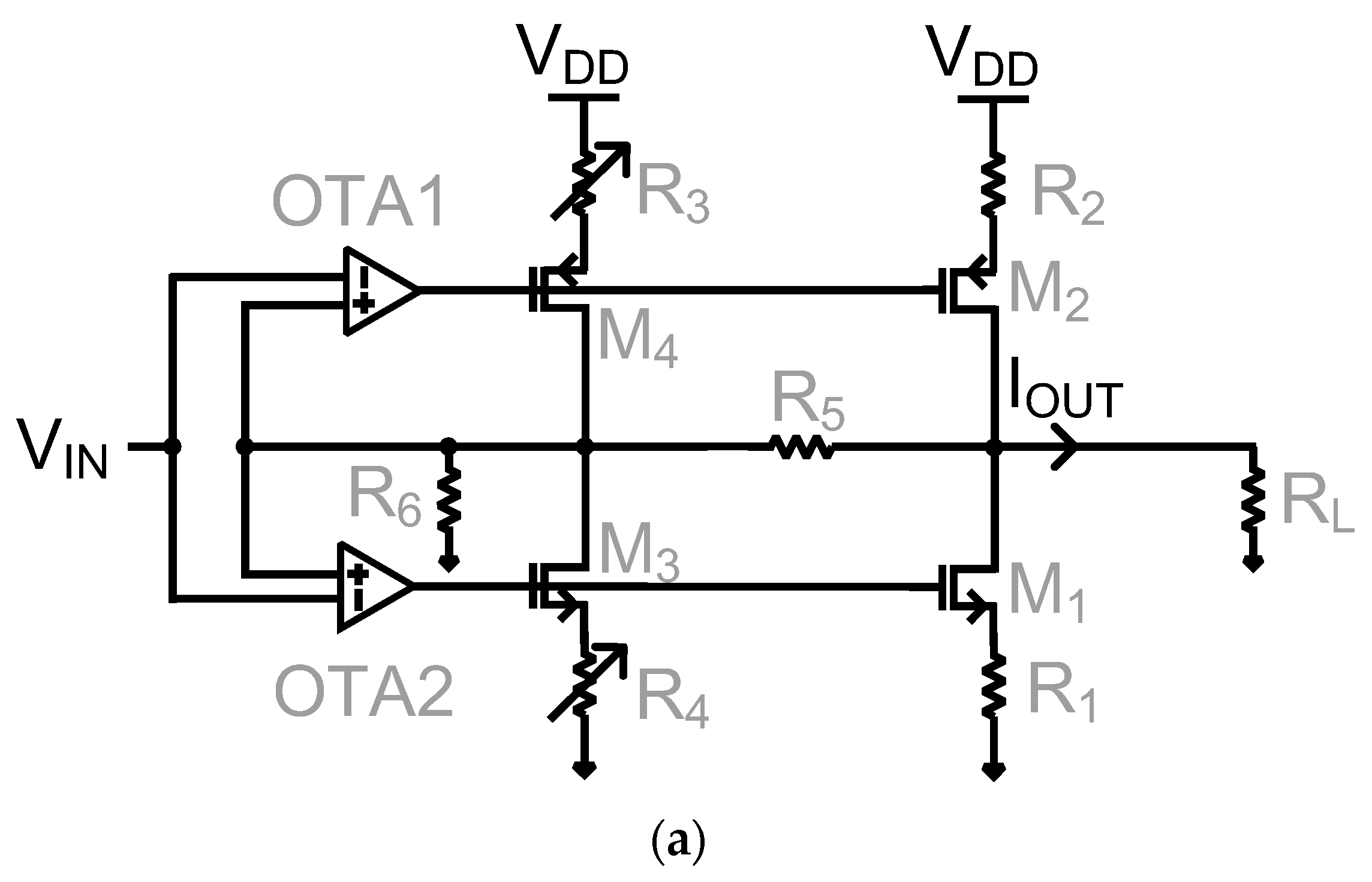
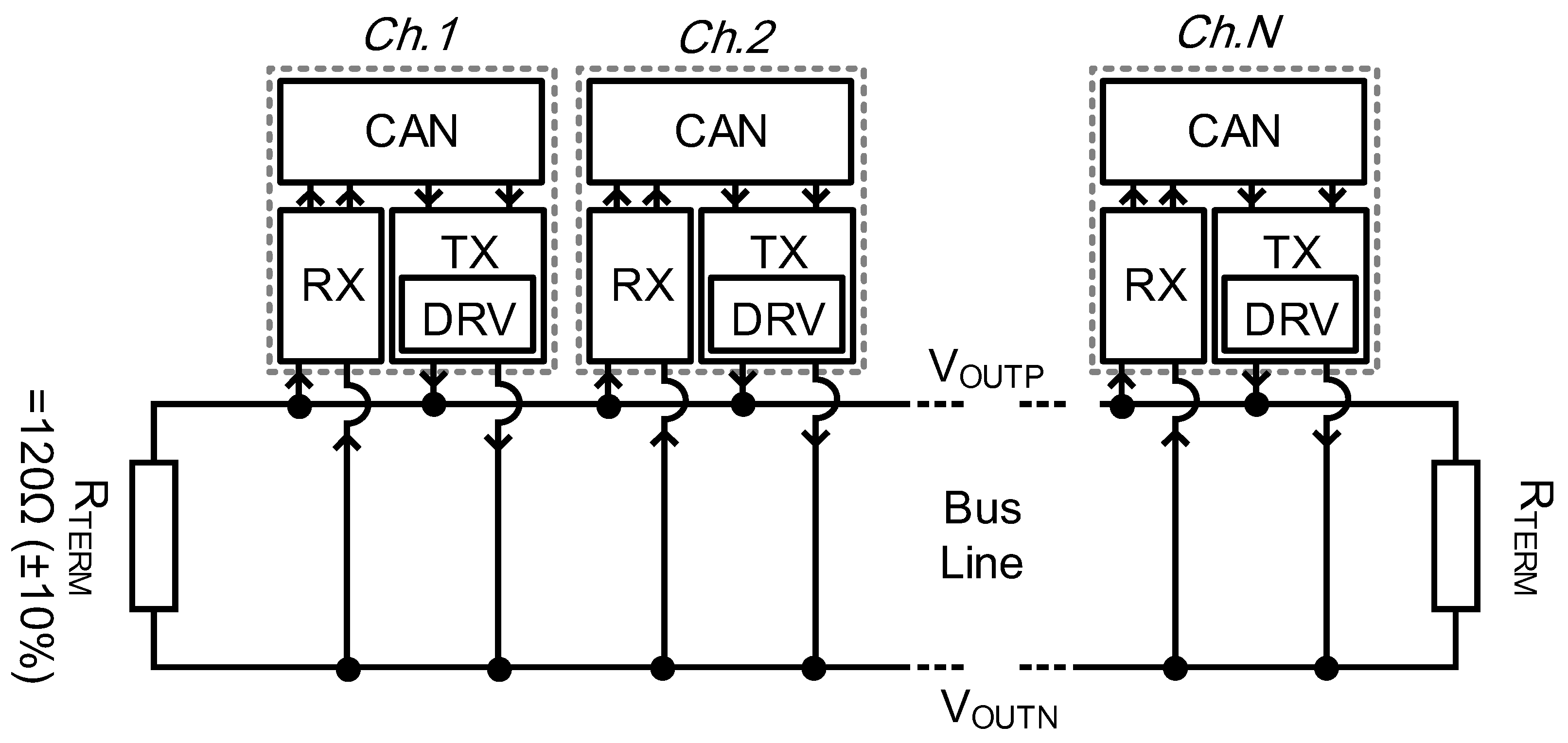
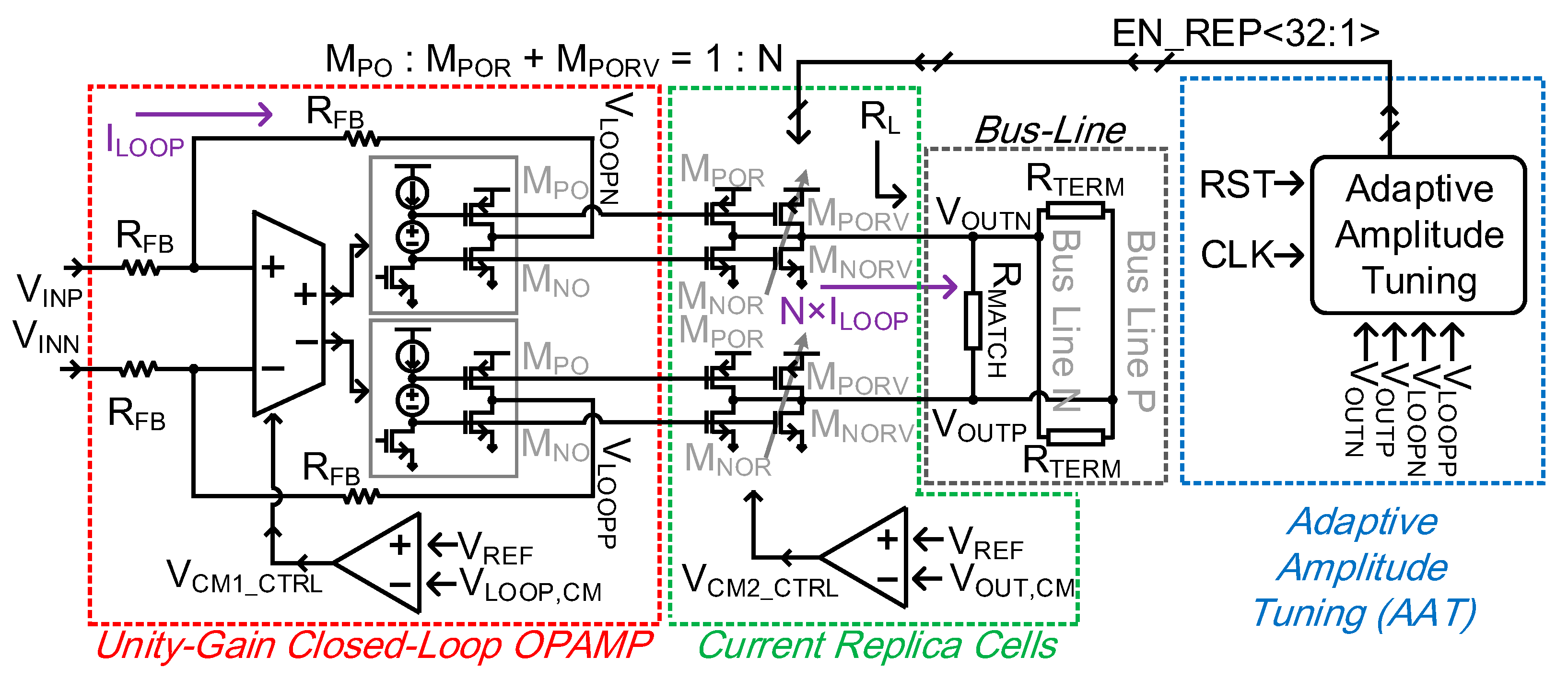
2.1. Architecture of the Hybrid of a Voltage- and a Current-Mode Line Driver

Figure 3 displays the overall block diagram of the proposed hybrid of a VMLD and CMLD, including an AAT. The proposed LD consists of two different blocks: a unity-gain closed-loop OPAMP and class-AB current replica cells. The unity-gain OPAMP converts input differential voltage signals to currents. The signal currents flow through the OPAMP’s output stage (MPO, MNO), and are replicated to the current replica cells (MPOR, MNOR, MPORV, and MNORV). The mirroring ratio N represents the replication ratio between MP(N)O and MP(N)OR + MP(N)ORV. The floating batteries MPBa,b and MNBa,b in Figure 4 define the shared gate-to-source voltage (VGS) of the OPAMP’s output stage and the replica cells. The VGS is defined with VFBP, VFBN, and the supply in Figure 3. The feedback resistor RFB should be set according to the mirroring ratio N and the output impedance RL, the impedance seen at termination resistor RTERM and the impedance matching resistor RMATCH in Figure 3. The OPAMP can drive the appropriate amount of signal currents by matching the RFB value to the equivalent load impedance (RL). The required value of RFB can be derived with the LD’s ideal closed-loop voltage gain (AV) as in Equation (1):
A V = V OUTP V OUTN V INP V INN = N 2 R FB ( R TERM · R MATCH R TERM + 2 R MATCH ) .
If N = 4, then RFB should be 60 Ω to guarantee a unity-gain (AV = −1) since RTERM = 120 Ω and RMATCH = 60 Ω.

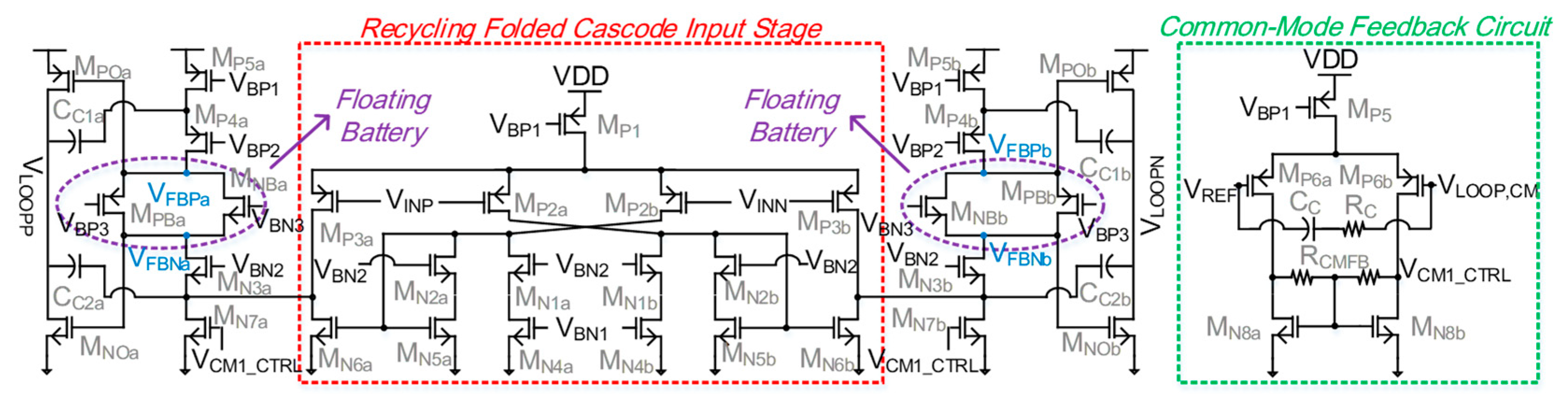
2.2. Architecture of the Operational Amplifier

Figure 4 describes the schematic of the OPAMP and its CMFB circuit. The two-stage OPAMP is designed with a recycling folded cascode architecture for the first input stage. Compared to the conventional folded cascode architecture, the recycling folded cascode can further improve slew-rate and input equivalent trans-conductance [12]. The improvements result in enhanced loop-gain and unity-gain frequency (UGF). In addition, the class-AB output stage with floating batteries guarantees better power-efficiency for the output stage. The CMFB is designed with local CMFB resistors RCMFB and null-resistor compensation. The null-resistor RC generates a left-half-plane (LHP) zero, which guarantees an enhanced common-mode phase margin (PM) [13]. In addition, two different CMFB loops are implemented in the proposed hybrid LD to set appropriate common-mode levels for both the closed-loop OPAMP and the current replica cells. VLOOP,CM and VOUT,CM are the common-mode voltages of the closed-loop OPAMP and the bus line voltages, respectively. The dual CMFB topology also allows a faster transient common-mode signal response, which results in enhanced signal linearity [5]. The OPAMP achieves differential-mode (DM) DC loop-gain, PM, and UGF of 64.1 dB, 57.2 degrees, and 517 MHz, respectively, in the nominal case. Table 1 displays the summary of the OPAMP’s DM AC performances over PVT variations and device mismatches.

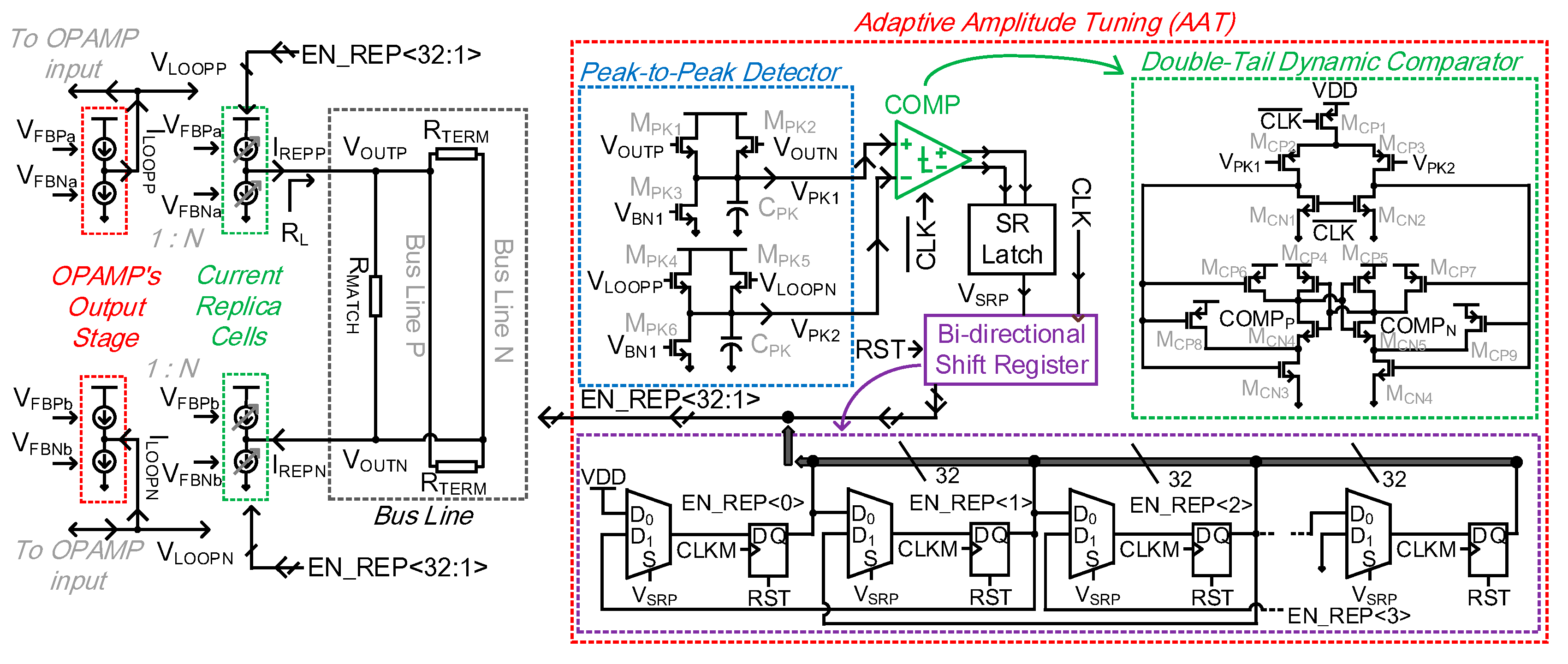
3. Adaptive Amplitude Tuning for Load Impedance Variations

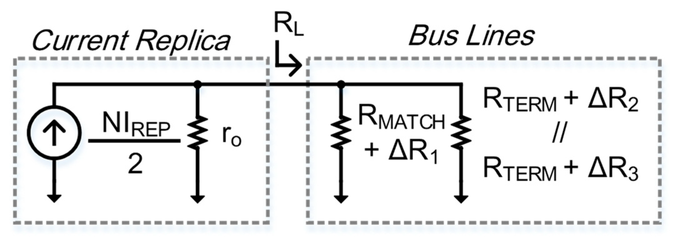
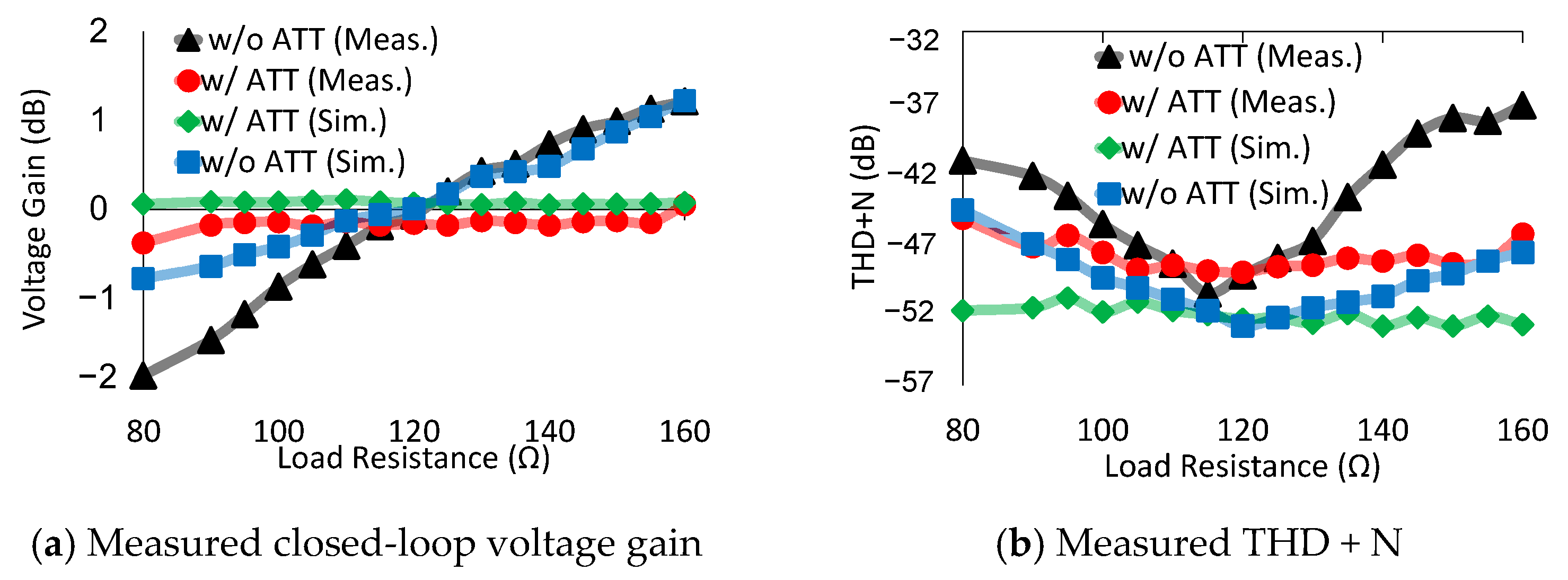
3.1. Effect of Load Impedance Variations on the Line Driver’s Performances

The OPAMP’s output stage and the current replica cells should ideally have equal input (Vgs) and output (Vds) voltages to guarantee an accurate mirroring ratio N for the signal currents and the enhanced signal linearity [8]. However, the equivalent load impedance (RL) in Figure 3 is vulnerable to process, temperature, the number of turned-on receivers, the input impedance of the receivers, and line lengths [1]. Figure 5 describes the small-signal model of the current replica cells and the bus lines including those variations. ΔR1, ΔR2, and ΔR3 represent the variations in RMATCH and each RTERM, respectively. The equivalent load variations generate different drain voltages between VLOOP and VOUT since the sizes of the signal currents replicated to the replica cells are defined by the feedback resistor RFB in the unity-gain closed-loop OPAMP block. Therefore, the variations result in a degraded linearity and non-unity closed-loop voltage gain.

3.2. Conventional Signal Linearity Enhancement and Signal Gain Control Techniques

Two different well-known LD techniques for load resistance variations are shown in Figure 6. A tunable current mirror technique [1] is implemented in Figure 6a with variable resistors R3 and R4. The OTA1–2, M1–4, and R1–2 are error amplifiers, class-AB output transistors, and fixed resistors, respectively. The LD’s output resistance can be implemented similarly to the load resistance RL if the variable resistors R3 and R4 are (n + 1)Rnom and nRnom, respectively, where the n and Rnom are the MOSFET size ratio between M3–4 and M1–2, and channel line resistance, respectively [1]. This technique enhances the LD’s signal linearity performance by achieving proper line termination matching. In addition, the voltage gain can be controlled by modifying the variable resistances R3–4 according to the load resistance RL variations. However, the tunable current mirror technique limits the LD’s maximum output voltage range due to the voltage drop on the resistors R1 and R2. A large amount of output current is typically demanded for the LDs, which cannot alleviate the voltage drop well by decreasing the variable resistances. In addition, the analogous characteristic does not allow area scaling against the modern short-channel technologies.
Another conventional LD technique [8] is shown in Figure 6b. A differential transconductance stage drives the differential class-AB output stage with slave current mirrors M1,4,5,8,9,13,12,16. The LD’s signal linearity is enhanced with cascode MOSFETs M2–3,6–7,10–11,14–15 and auxiliary operational transconductance amplifiers OTA1–4 by effectively shielding the slave current mirrors’ drain nodes [8]. Although the techniques can further improve the signal linearity by boosting the LD’s output resistances, the cascode MOSFETs limit the LD’s maximum output voltage level. In addition, the linearity enhancement techniques increase the quiescent current consumption due to the auxiliary amplifiers and the cascode stage’s extra bias circuit branches.

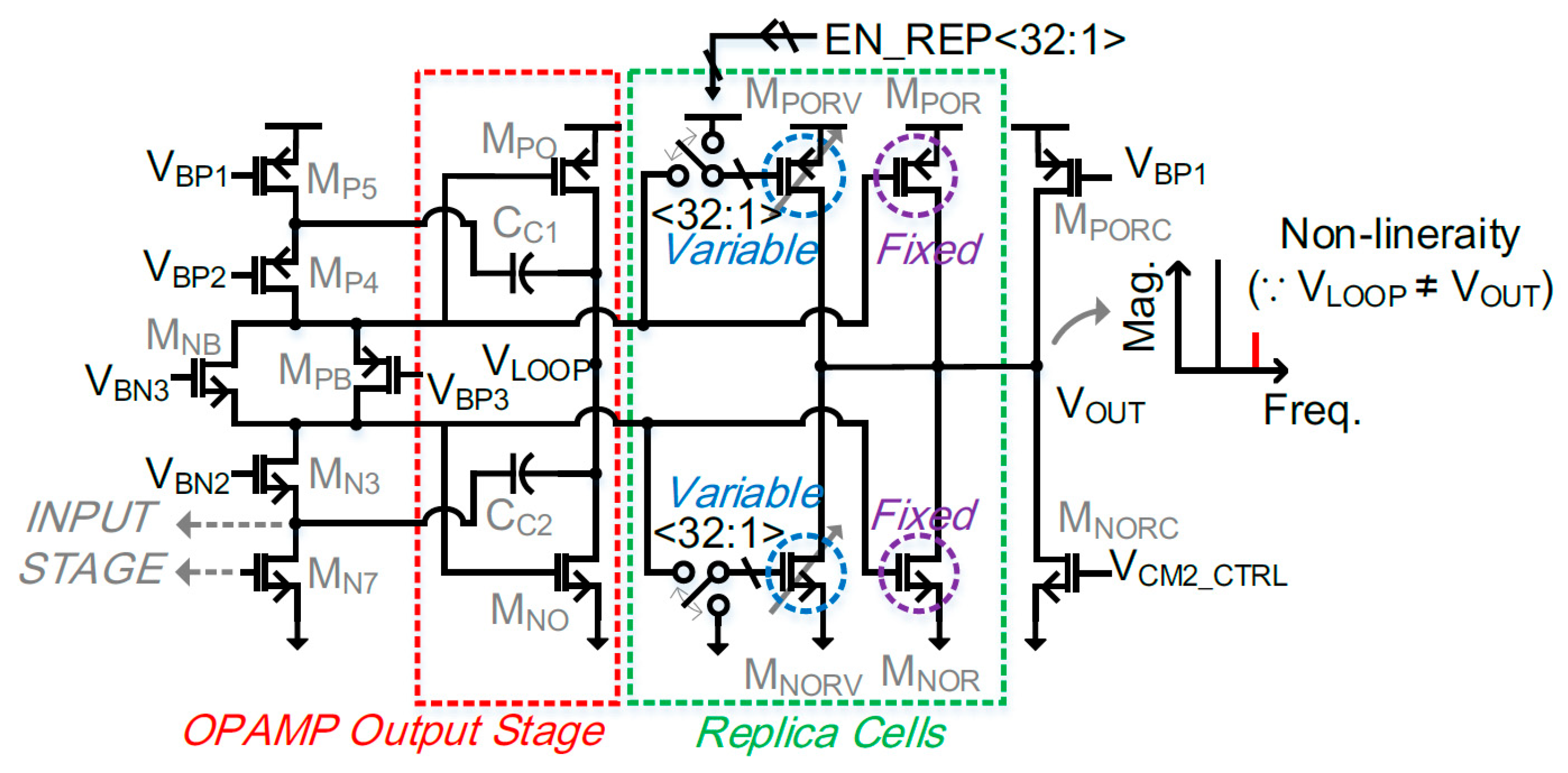
3.3. Proposed Signal Linearity Enhancement and Signal Gain Control Technique

The two major problems of the conventional LD’s linearity enhancement and signal gain control techniques are output voltage range limitation and extra quiescent power consumption. A digital-based adaptive amplitude tuning (AAT) technique is proposed to guarantee robust signal linearity and closed-loop gain variations against the load variations without limiting the LD’s maximum output voltage level and without adding extra quiescent current consumption. Figure 7 displays the connection between the OPAMP’s cascode stage, the OPAMP’s output stage, and current replica cells. The replica cells consist of two different class-AB current source/sink stages. MP(N)ORV represents a variable-size stage while MP(N)OR is a fixed-size stage. The number of turned-on variable replica cells is denoted as N in Figure 5. The closed-loop voltage gain can be controlled by controlling the sizes of the variable replica cells MPORV and MNORV. When the load impedance increases (=ΔR2,3 is positive), then the output voltage increases without the AAT function since the loop current (ILOOP) (in Figure 3) stays unchanged. However, the AAT turns off some of the variable current replica cells (= decrease N) to deliver a reduced ILOOP to the bus lines. When the load impedance decreases (=ΔR2,3 is negative), the N increases, and vice versa, to sustain the unity gain (AV = −1) as in Equation (2):
A V = N 2 R FB [ r o | | ( R MATCH + Δ R 1 ) | | ( R TERM + Δ R 2 ) | | ( R TERM + Δ R 3 ) ]
The replica cells’ output impedance ro is approximately a few mega-ohms, which is comparably negligible in Equation (2). The unity-gain property not only mitigates the close-loop gain variations, but also alleviates signal linearity variations since the proposed AAT keeps the output voltages VLOOP and VOUT the same. In addition, the current replica cells prevent the OPAMP’s stability, bandwidth and loop-gain variations against the RL variations since the current replica cells act as buffers between the OPAMP and the bus lines. The 32-bit thermometer digital code EN_REP controls the number of turned-on variable replica cells. In this design, the number of gate fingers for MP(N)O, MP(N)ORV, and MP(N)OR are 32, 32, and 112, respectively, with an identical unit finger MOSFET size. The mirroring ratio N is set at 4 when EN_REP is set at mid-code.
The overall block diagram of the proposed AAT is shown in Figure 8. One peak-to-peak detector determines the peak of the OPAMP loop voltage VPK1 with the loop voltages VLOOPP and VLOOPN. Another peak-to-peak detector determines the peak of the channel voltage VPK2 with two line output voltages VOUTP and VOUTN. A double-tail dynamic comparator called COMP then compares the two peaks. The differential output of the comparator passes through a set–reset (SR) latch and enables each binary datum in the thermometer-based bi-directional shift register (BDSR). Each flip-flop (FF) in the BDSR is reset with an RST signal in the beginning. A decrease in the load impedance implies VPK1 < VPK2. The output of the comparator then becomes low, and the BDSR outputs (EN_REP) increase; this increases VPK1 and VOUT. When VPK1 > VPK2, the comparator’s output becomes high and EN_REP decreases. Afterward, the comparator’s output repeats low and high since VPK1 and VPK2 are crossing each other in the settled calibration region. The time-domain waveform is demonstrated in Figure 9 with a clock frequency of 5 MHz. In addition, the comparator features 6.32 mV for maximum offset voltage according to 1000-run mismatch Monte Carlo simulation. According to simulation results, the offset induces 1–2 bit errors in the BDSR output EN_REP, which results in approximately 0.7 dB THD degradation. The offset issue can be further alleviated with an offset calibration.

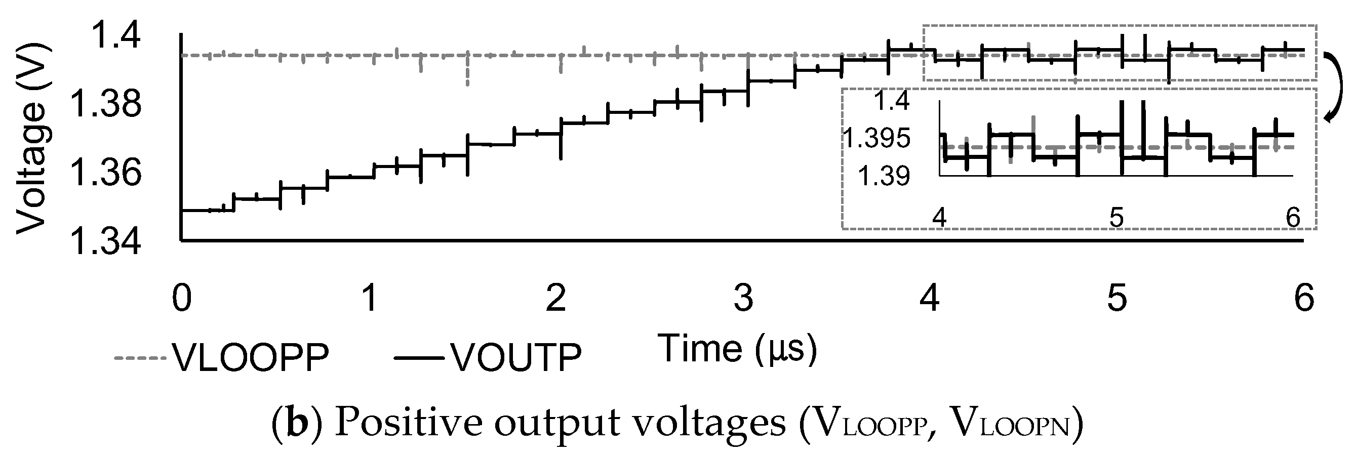
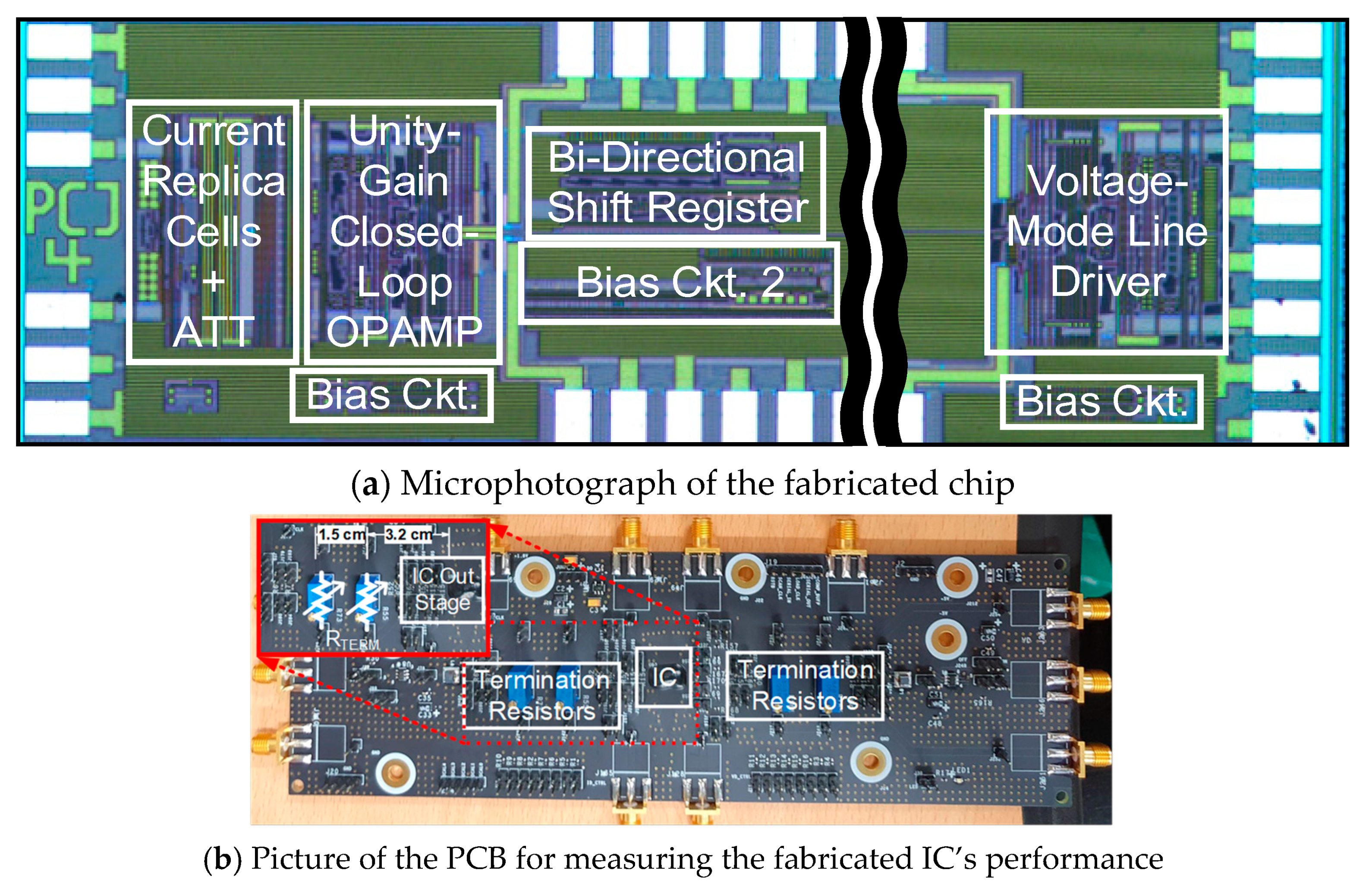
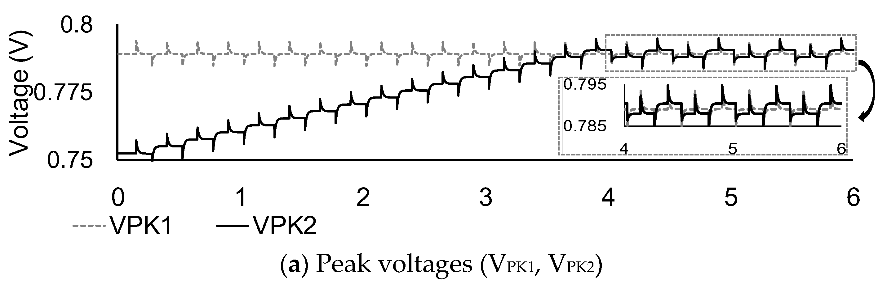
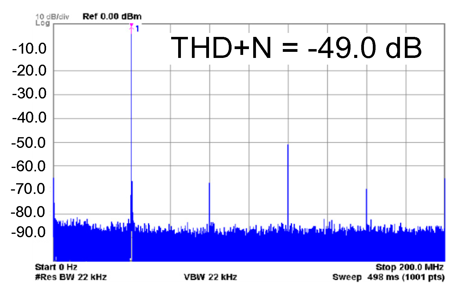
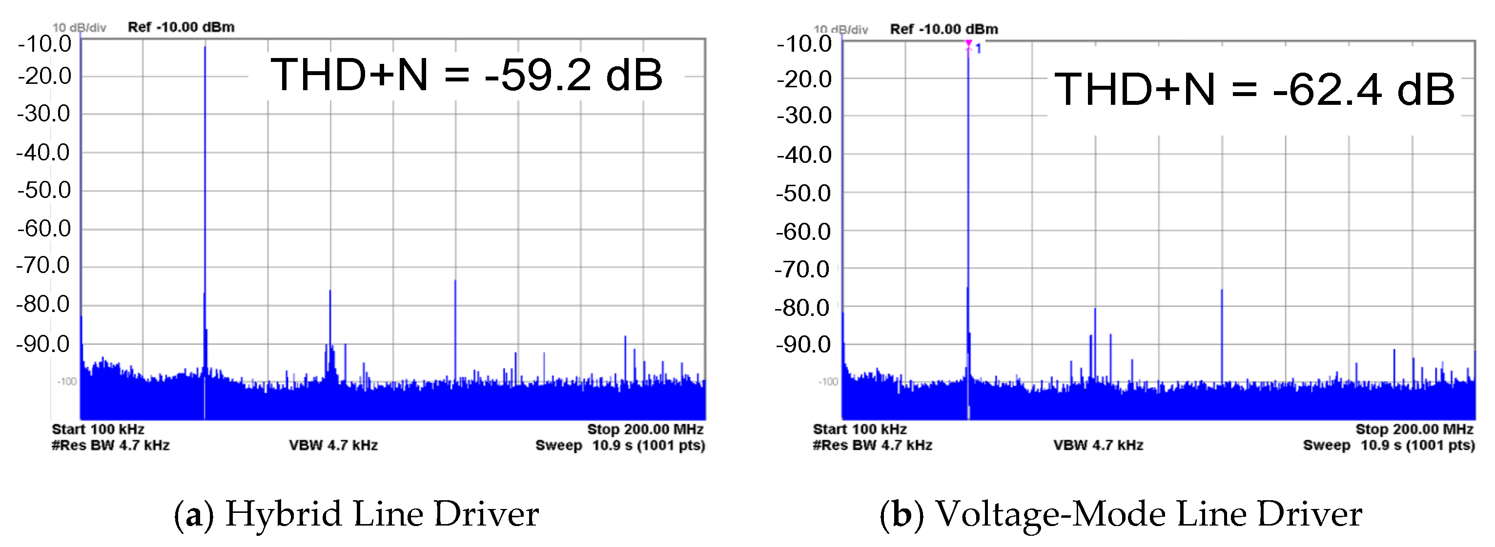
4. Measurement Results

The proposed hybrid of a VMLD and CMLD, and a conventional VMLD were fabricated in CMOS 180 nm to compare their performances. The microphotograph of the manufactured chip is shown in Figure 10a. The drivers are measured with a 1:1 impedance transformer to convert the differential output to single-ended for a signal analyzer [5]. A low-distortion high-speed analog buffer (OPA653) is implemented to prevent the chip’s load condition from being distorted with a signal analyzer’s (Keysight N9010A) 50 Ω input resistance. A vector signal generator (Agilent N5182A) generates an input signal. Figure 10b displays the manufactured printed circuit board (PCB) for testing the fabricated integrated circuits (ICs). The left and right sides of the PCB are designed to test the hybrid LD and VMLD, respectively. Each termination resistor is realized with discrete variable components (RTERM in Figure 10b) to alter its value to validate how well the ATT block prevents the proposed line driver’s performance from the channel load impedance variations. The channel lines are designed differentially, and they are designed to have the same line width and length on the positive and negative channels. The output stages of the proposed drivers are matched with the channel lines using series and parallel matching resistors for the VMLD and the hybrid LD, respectively.
The VMLD is designed with the conventional topology in Figure 2. The VMLD’s OPAMP architecture is the same as the one in Figure 4 for a fair comparison. The sizes of both class-AB output stages in both topologies are designed identically. Figure 11 displays the FFT of the proposed hybrid LD, and it achieves THD+N of −49.0 dB with an input frequency of 40 MHz and the maximum allowable output swing of 2.8 Vpp differential. The hybrid LD achieves a competitive THD+N of −59.2 dB against the VMLD, which achieves −62.4 dB THD+N with the same supply voltage of 1.8 V, as shown in Figure 12. They are measured with the same input frequency of 40 MHz and 930 mVpp differential signal swing on the bus lines, which is the maximum allowable channel swing for the VMLD. The VMLD features slightly enhanced linearity because the equivalent load (eq. RLOAD) for the hybrid LD is 30 Ω while the VMLD has 60 Ω due to the series source terminations. Lower load impedance requires a better current driving capability to source a larger amount of currents. However, the VMLD suffers from the series matching signal attenuation; therefore, the hybrid LD allows enhanced signal power to be delivered to the load with the same power supply voltage. The proposed LD achieves ηpower of 87.0%, while the VMLD achieves ηpower of only 7.22%.
Figure 13a describes the measured closed-loop voltage gain against the equivalent load impedance variations according to both simulation and measurement results. The load impedance variations change the closed-loop gain since the feedback resistors define the proposed hybrid LD’s output signal current levels. Without the ATT, the closed-loop gain varies from −1.87 dB to 1.21 dB. On the other hand, the calibration allows reduced closed-loop gain variations, which range from −0.38 dB to 0.05 dB. The calibration logic also prevents the driver’s linearity variations against the load variations, as shown in Figure 13b. The THD+N varies from −37.2 dB to −49.2 dB without the AAT. However, the AAT mitigates the THD+N variations from −45.2 dB to −49.0 dB by adjusting the variable replica cells in a range of 80–160 Ω load impedance variations. The AAT consumes 12.6 μW at FCLK = 5 MHz, which is almost negligible compared to the hybrid LD’s power consumption. This dynamic power can be further reduced by decreasing the clock frequency since the AAT does not have to operate quickly, depending on the required maximum calibration time.
Table 2 compares the proposed LD with the prior arts. The comparison table is filled with the prior arts that are tested with similar megahertz bandwidth levels and resistive load conditions to keep the fairness against the signal bandwidth and the load condition. The proposed hybrid LD features the best ηpower, which stands for a ratio between the signal power delivered to the load (PL) compared to the consumed quiescent power (PQ). This is because the current mode prevents signal attenuation with the parallel termination impedance matching. The proposed hybrid LD and VMLD consume 37.6 mW and 25.2 mW while delivering PL of 32.7 mW and 1.82 mW, respectively. A figure of merit (FoM) from reference [14] is used to evaluate the line drivers’ performances as follows in Equation (3):
FoM = P L P Q × ( THD + N [ % ] )
The FoM features the power efficiency and signal linearity of the line driver. The hybrid LD in this work achieves an FoM of 1.58, which is the best FoM among the table. The VMLD features a lower FoM of 0.95. The proposed hybrid LD allows a wide output swing on the output channels, and features the best ηpower. The comparably large area consumption is one of the noticeable weaknesses of the proposed hybrid line driver. Fortunately, this issue can be alleviated by using more recent short-channel technologies. This is because the AAT logic is digital, whose area decreases as the technology shrinks, while the previous analog mechanisms typically do not.

5. Discussion and Conclusions

In this paper, a hybrid of a voltage-mode and a current-mode line driver with adaptive amplitude tuning for a turbo controller area network is presented. The hybrid line driver consists of a unity-gain closed-loop OPAMP and class-AB current replica cells. The proposed line driver prevents the signals from impedance matching attenuation by implementing parallel source termination. In addition, the adaptive amplitude tuning controls the sizes of the current replica cells to alleviate closed-loop voltage gain and signal distortion variations against the load impedance variations. The proposed tuning mechanism does not cause any extra quiescent current consumption but rather a small amount of dynamic power, and it also does not degrade the maximum allowable output voltage range, which are major problems on conventional signal linearity enhancement and voltage gain control techniques. The proposed hybrid driver is manufactured in CMOS 180 nm, and it achieves −49.0 dB THD+N at an input frequency of 40 MHz and 0.99 peak-to-peak rms output voltage with 32.7 mW power consumption from 1.8 V supply voltage. The conventional voltage-mode driver is also manufactured with the same technology, and it features −62.4 dB THD+N at the same input frequency and 1/3 attenuated output rms voltage range with 25.2 mW power consumption from the same 1.8 V supply voltage. In the manner of signal linearity, power consumption, output signal swing, and the resistive load condition, the proposed hybrid driver achieves 1.58 figure-of-merit (FoM) while the conventional voltage-mode driver and the best FoM among prior arts are 0.95 and 0.46, respectively.

Author Contributions

Conceptualization, C.P.; methodology, C.P.; software, C.P.; validation, C.P.; formal analysis, C.P.; investigation, C.P.; resources, C.P.; data curation, C.P.; writing—original draft preparation, C.P.; writing—review and editing, C.P.; visualization, C.P.; supervision, M.L.; project administration, M.L.; funding acquisition, M.L. All authors have read and agreed to the published version of the manuscript.

Funding

This work was supported in part by the Institute of Information & Communications Technology Planning & Evaluation (IITP) grant funded by the Korea government (MSIT) [No. 2019-0-01348, High-speed, high-reliability, and intelligent IVN (In-Vehicle Network) semi-conductor development]. The EDA tool was supported by the IC Design Education Center (IDEC), Korea.

Conflicts of Interest

The authors declare no conflict of interest.

References

  1. Ramachandran, N.; Dinc, H.; Karsilayan, A. A 3.3-V CMOS adaptive analog video line driver with low distortion performance. IEEE J. Solid-State Circuits 2003, 38, 1051–1058. [Google Scholar] [CrossRef]
  2. Babanezhad, J.N. A 100-MHz, 50-Ω, -45-dB distortion, 3.3-V CMOS line driver for Ethernet and fast Ethernet net-working applications. IEEE J. Solid-State Circuits 1999, 34, 1044–1050. [Google Scholar] [CrossRef]
  3. Ara, B.; Kim, C.-S.; Lee, S.-S. A CMOS line driver for ADSL central office applications. IEEE J. Solid-State Circuits 2003, 38, 2201–2208. [Google Scholar]
  4. Liu, P.-K.; Hung, S.-Y.; Liu, C.-Y.; Hsieh, M.-H.; Chen, C.C.-P. A 52 dBc MTPR line driver for powerline communication HomePlug AV standard in 0.18-μm CMOS technology. In Proceedings of the 2013 IEEE International Symposium on Circuits and Systems (ISCAS2013), Beijing, China, 19–23 May 2013; pp. 1404–1407. [Google Scholar] [CrossRef]
  5. Zhu, Z.; Wang, J. A Compact High-Performance Programmable-Gain Analog Front End for HomePlug AV2 Communication in 0.18 um CMOS. IEEE Trans. Circuits Syst. I Regul. Pap. 2017, 64, 1–13. [Google Scholar] [CrossRef]
  6. Johns, D.; Essig, D. Integrated circuits for data transmission over twisted-pair channels. IEEE J. Solid-State Circuits 1997, 32, 398–406. [Google Scholar] [CrossRef]
  7. Hadidi, K.; Oshima, H.; Sasaki, M.; Matsumoto, T. A highly linear fully differential low power CMOS line driver. In Proceedings of the ESSCIRC 2004—29th European Solid-State Circuits Conference (IEEE Cat. No.03EX705), Estoril, Portugal, 16–18 September 2004; pp. 541–544. [Google Scholar] [CrossRef]
  8. Pan, H.; Yao, Y.; Hammad, M.; Tan, J.; Abdelhalim, K.; Wang, E.W.; Hsu, R.C.J.; Tam, D.; Fujimori, I. A Full-Duplex Line Driver for Gigabit Ethernet with Rail-to-Rail Class-AB Output Stage in 28 nm CMOS. IEEE J. Solid-State Circuits 2014, 49, 3141–3155. [Google Scholar] [CrossRef]
  9. Mahadevan, R.; Johns, D. A differential 160-MHz self-terminating adaptive CMOS line driver. IEEE J. Solid-State Circuits 2000, 35, 1889–1894. [Google Scholar] [CrossRef]
  10. Sung, G.-M.; Chou, W.-D.; Yu, C.-P. A 10-bit 1.8 V 45 mW 100 MHz CMOS transmitter chip for use in an XDSL modem in a home network. Analog. Integr. Circuits Signal Process. 2014, 81, 515–527. [Google Scholar] [CrossRef]
  11. Kang, S.; Han, S.; Cho, S.; Jang, D.; Choi, H.; Choi, J.-W. High speed CAN transmission scheme supporting data rate of over 100 Mb/s. IEEE Commun. Mag. 2016, 54, 128–135. [Google Scholar] [CrossRef]
  12. Rida, S.A.; Silva-Martinez, J. The recycling folded cascode: A general enhancement of the folded cascode am-plifier. IEEE J. Solid-State Circuits 2009, 44, 2535–2542. [Google Scholar]
  13. Dasgupta, U. Low voltage 2-stage and 3-stage push-pull output amplifiers in 65-nm CMOS technology. In Proceedings of the 2016 International Symposium on Integrated Circuits (ISIC), Sinapore, 12–14 December 2016; pp. 1–4. [Google Scholar] [CrossRef]
  14. Nandish, M.; Huijsing, J.H.; Stojanović, V. A 1-mW Class-AB Amplifier With− 101 dB THD+ N for High-Fidelity 16 Ω Headphones in 65-nm CMOS. IEEE J. Solid-State Circuits 2019, 54, 948–958. [Google Scholar]
Figure 1. Architecture of a voltage-mode line driver.
Electronics 10 01785 g001
Figure 2. Block diagram of controller area network (CAN).
Electronics 10 01785 g002
Figure 3. Block diagram of the proposed current-mode line driver with an adaptive amplitude tuning.
Electronics 10 01785 g003
Figure 4. Schematic of the rail-to-rail output two-stage recycling folded cascode OPAMP including the CMFB circuit (bias circuit is omitted for simplicity).
Electronics 10 01785 g004
Figure 5. Small-signal model of the current replica cells and the bus line.
Electronics 10 01785 g005
Figure 6. Conventional signal linearity enhancement and signal gain control techniques. (a) Line driver using error amplifiers and tunable current mirrors [1]. (b) A current-mode H-bridge class-AB output stage with auxiliary amplifiers [8].
Electronics 10 01785 g006aElectronics 10 01785 g006b
Figure 7. Schematic of the OPAMP’s output stage and current replica cell.
Electronics 10 01785 g007
Figure 8. Block diagram of adaptive amplitude tuning with the OPAMP class-AB output stage and current replica cell with bus lines.
Electronics 10 01785 g008
Figure 9. Simulated waveform of the proposed adaptive amplitude tuning at DC.
Electronics 10 01785 g009aElectronics 10 01785 g009b
Figure 10. Microphotograph and test board of the fabricated chip.
Electronics 10 01785 g010
Figure 11. Measured FFT and THD+N of the proposed hybrid line driver at FIN = 40MHz and output swing of 2.8 VPP differential.
Electronics 10 01785 g011
Figure 12. Measured THD+N of the proposed hybrid line driver, and the conventional voltage-mode line driver at FIN = 40 MHz and 930 mVPP differential of signal swing on the bus lines.
Electronics 10 01785 g012
Figure 13. Simulated and measured closed-loop voltage gain (AV) and THD + N of the hybrid line driver against load resistance variations at FIN = 40MHz and output swing of 2.8 VPP differential.
Electronics 10 01785 g013
Table 1. The OPAMP’s AC Performances over PVT Variations and 1000-Run Monte-Carlo Simulation Results over Device Mismatches.
Process Variations
TTSSFFSFFS
Loop Gain at DC [dB]64.16861.364.963.4
Phase Margin [deg.]57.257.257.955.159.3
Unity-Gain Frequency [MHz]517468568530501
Temperature Variations [°C]
−4027125
Loop Gain at DC [dB]67.464.159.5
Phase Margin [deg.]54.357.260.1
Unity-Gain Frequency [MHz]622517395
Supply Voltage Variations [V]
1.621.81.98
Loop Gain at DC [dB]62.464.165.2
Phase Margin [deg.]57.657.255.9
Unity-Gain Frequency [MHz]457517562
1000-Run Monte-Carlo Mismatch Simulation
MeanStandard Deviation
Loop Gain at DC [dB]64.10.808
Phase Margin [deg.]57.31.13
Unity-Gain Frequency [MHz]51616.0
Table 2. Proposed Line Driver’s Performance Comparison with Prior Art.
This Work
(Hybrid LD)
This Work
(VMLD)
[1][7][9][10]
Process180 nm180 nm500 nm180 nm350 nm180 nm
Supply [V]1.81.8±1.652.53.31.8
VOUT [VPP,rms]0.990.330.851.061.411.24
Eq. RLOAD [Ω]3060757575100
PQ [mW]37.625.226.413015538.6
Driving Mode 1I+VVIVII
PL [mW]32.71.8219.215.626.630.6
ηpower [%]87.07.2236.51217.239.8
THD+N [dB]−49.0−62.4−42−51.2−42−48
THD+N [%]0.550.07590.7940.2750.7940.398
FIN [MHz]404051030100
Area [mm2]0.3770.1330.220.0940.2100.48
FoM1.580.950.460.420.221.00
1 I: current-mode LD, V: voltage-mode LD, I + V: hybrid of voltage- and current-mode LD.
Publisher’s Note: MDPI stays neutral with regard to jurisdictional claims in published maps and institutional affiliations.

