
Optimization and Design of Passive Link with Single Channel 25 Gbps Based on High-Speed Backplane


Abstract
:1. Introduction
2. Materials and Methods
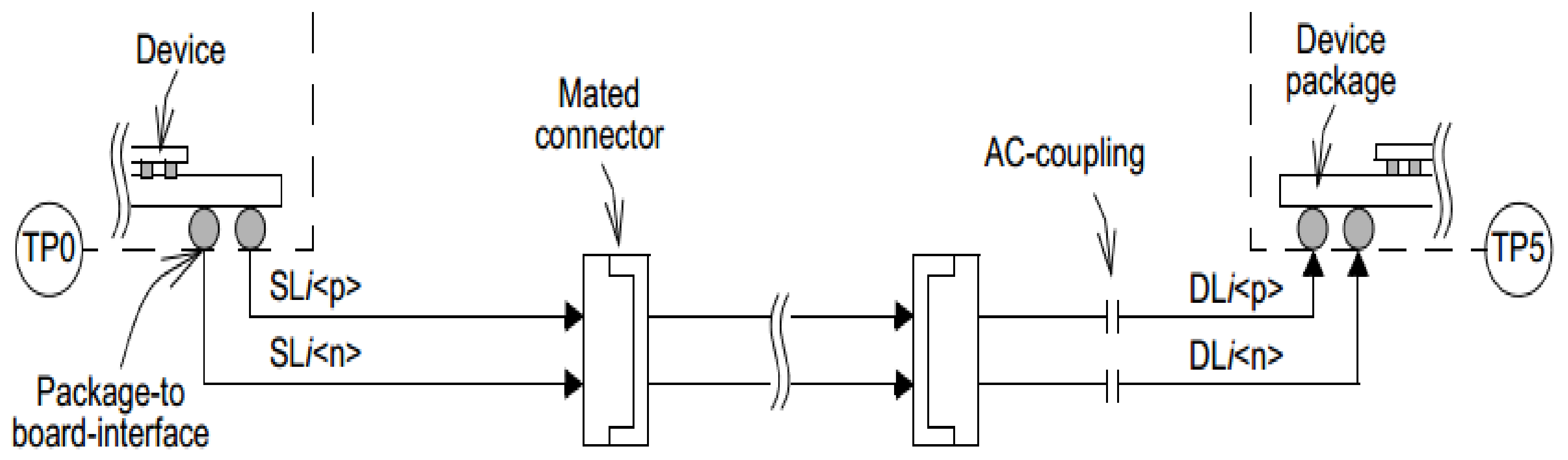
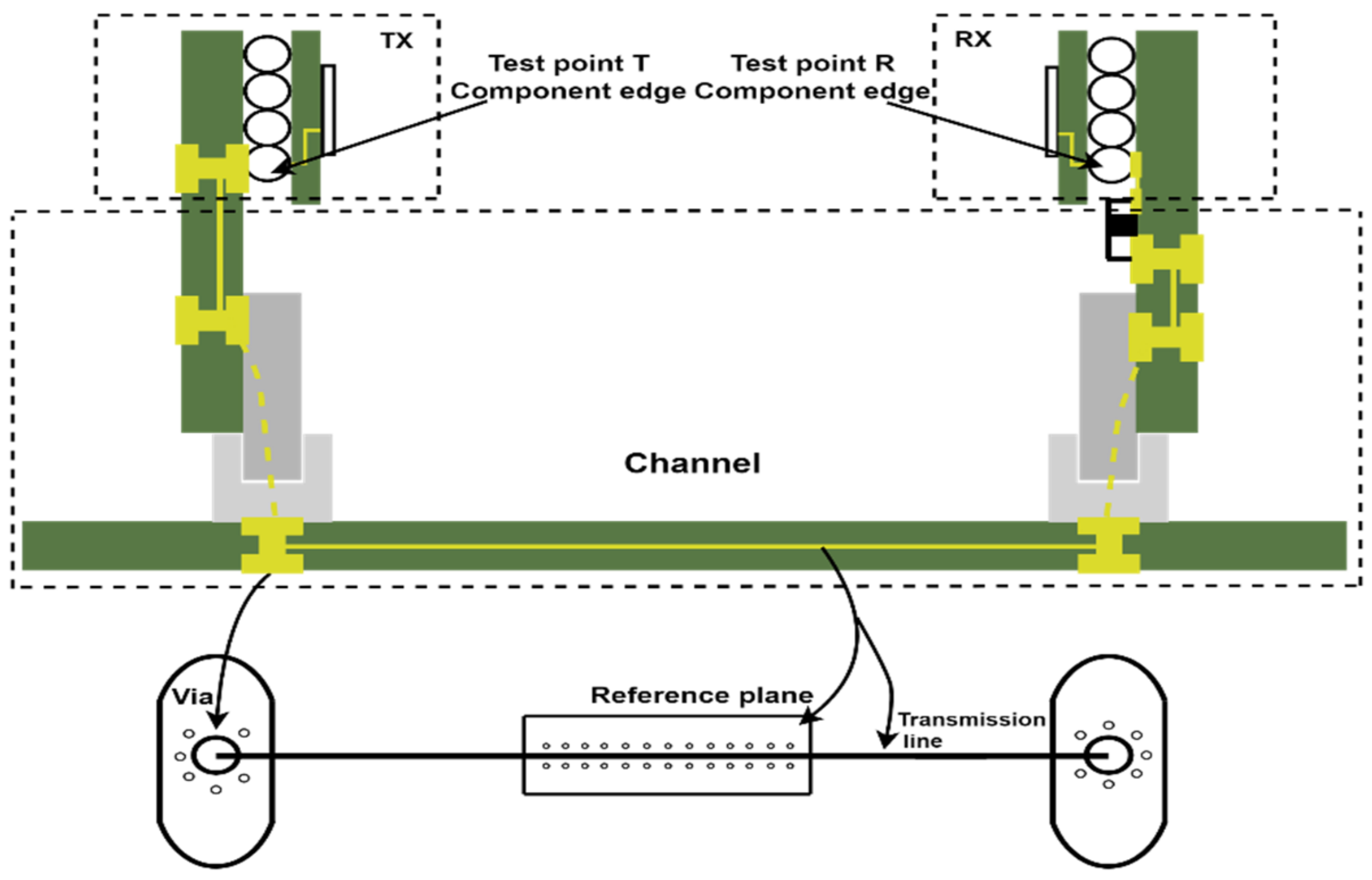
2.1. System Composition
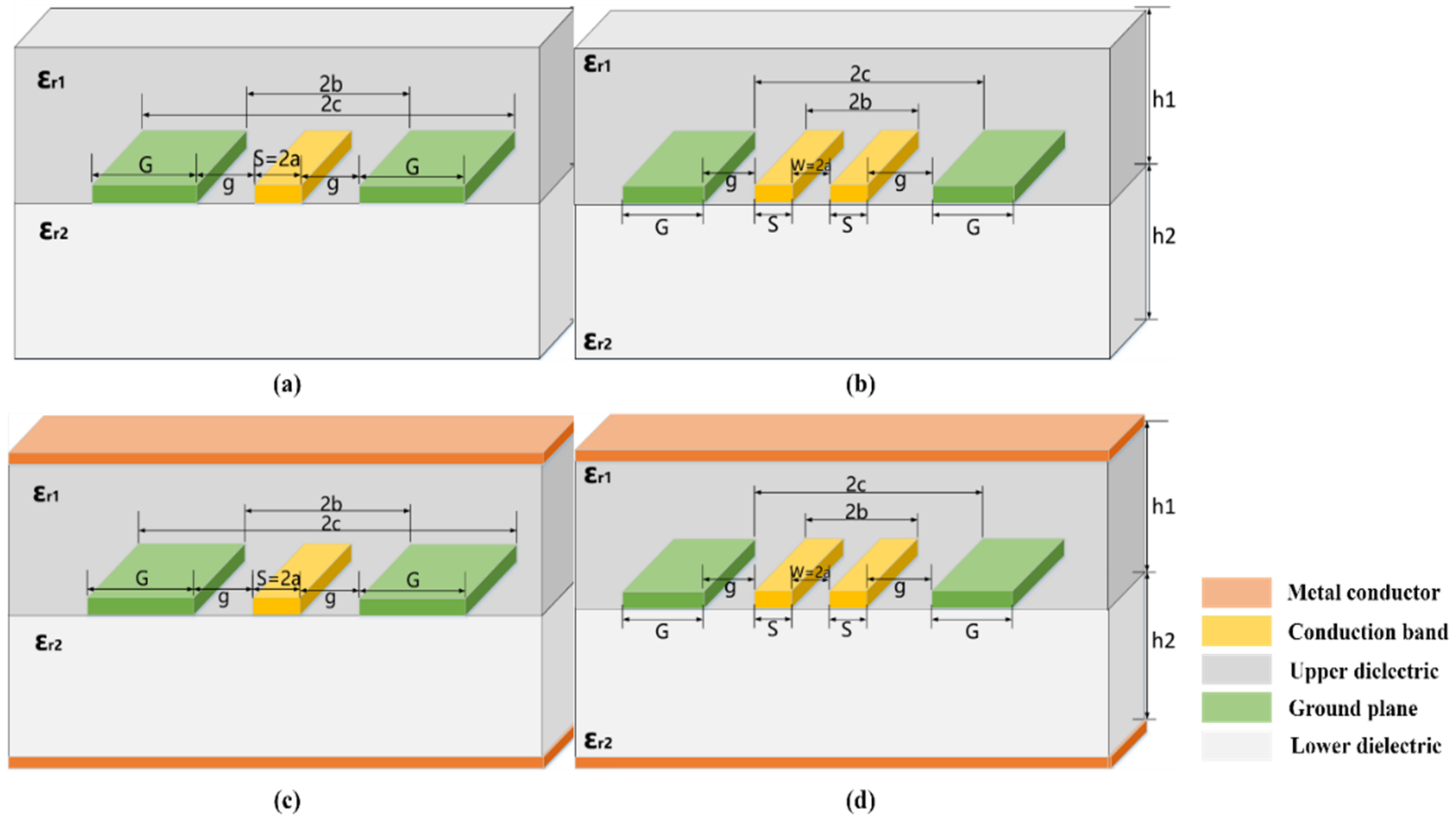
2.2. Strip Coplanar Waveguide Transmission Line
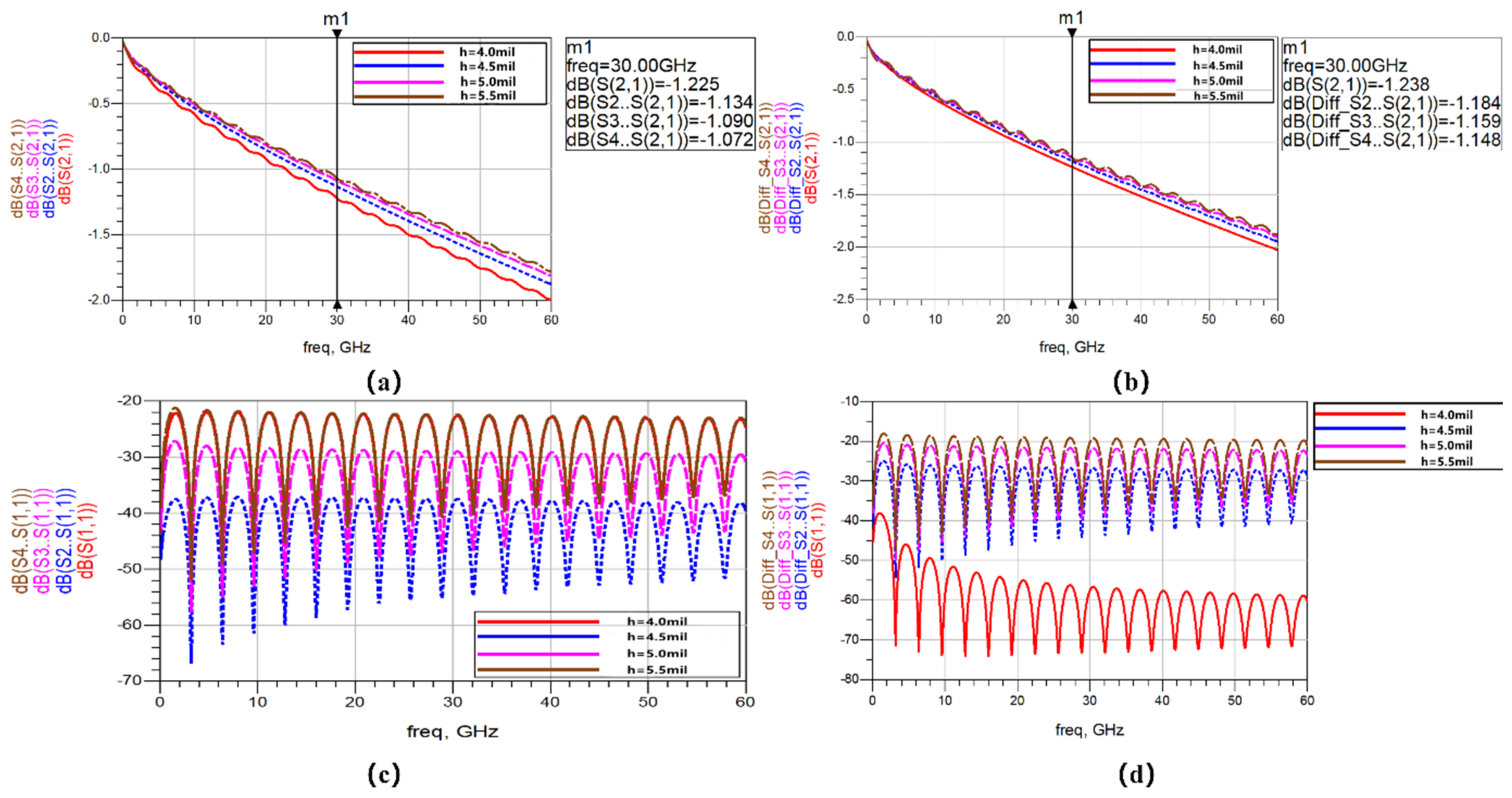
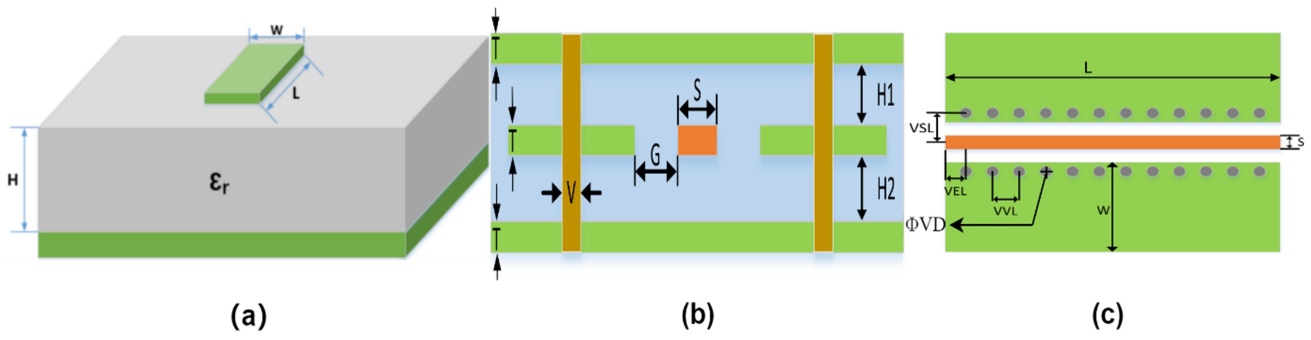
Modeling and Analysis of Strip Coplanar Waveguide
2.3. Research on Transmission Line Reference Plane for 25 Gbps Rate Backplane
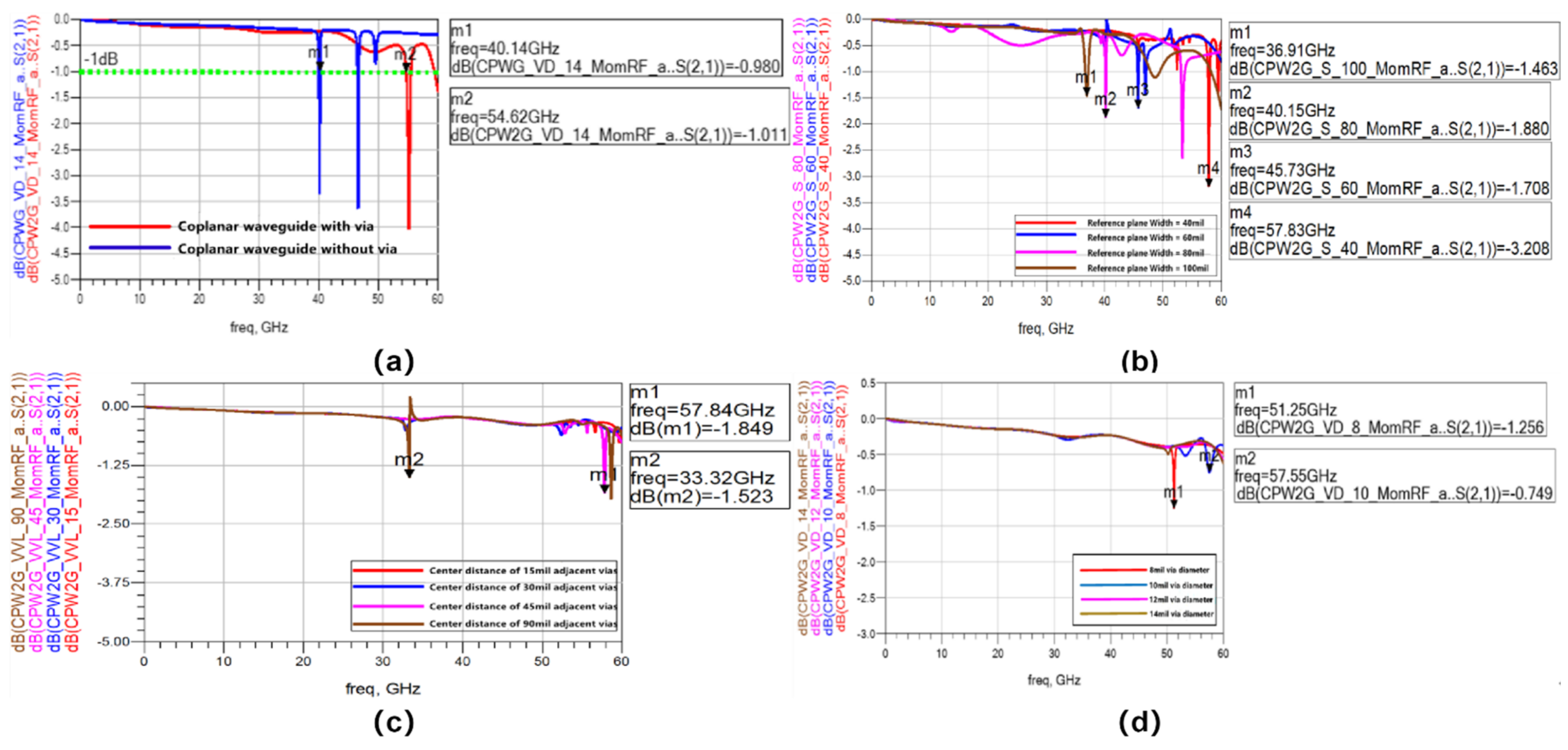
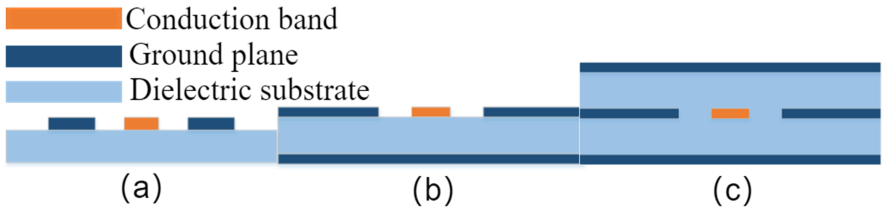
Coplanar Waveguide Reference Plane Modeling
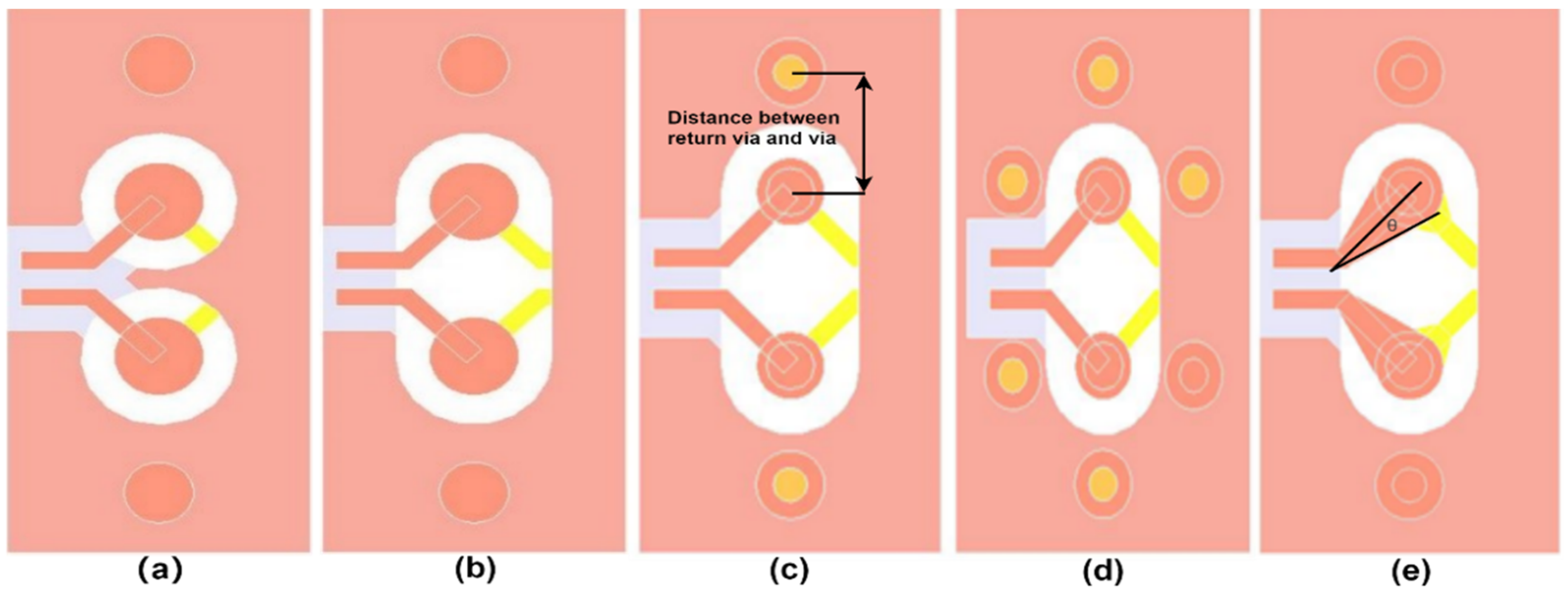
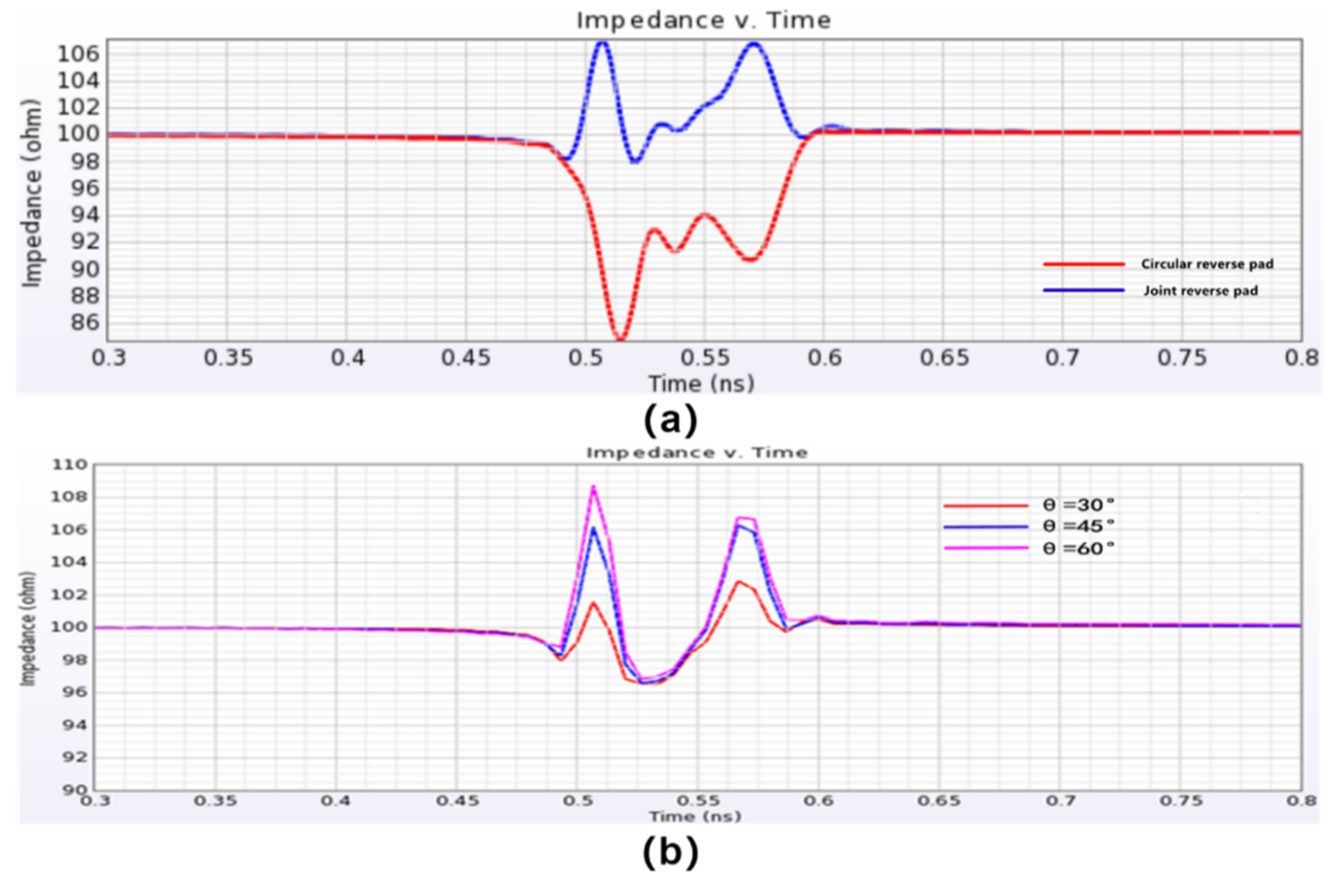
2.4. Research on Via for 25 Gbps Rate Backplane
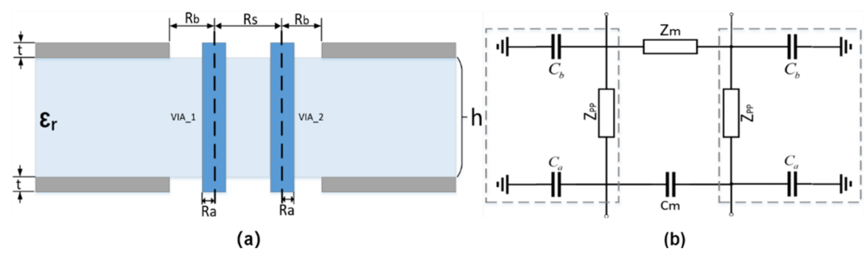
Modeling and Analysis
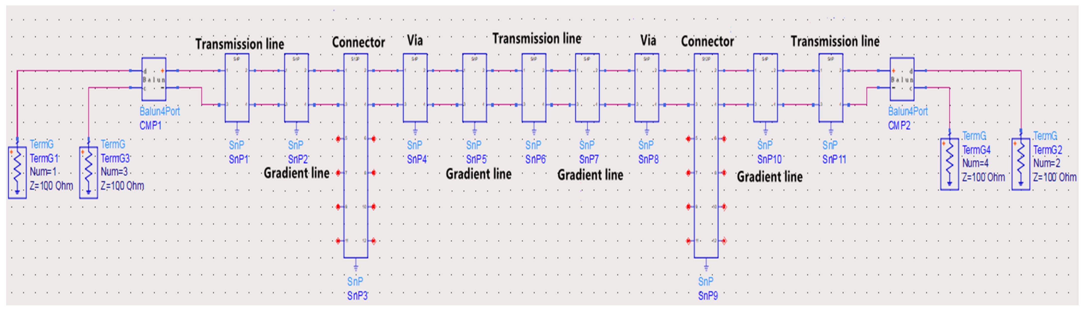
2.5. Composition of Backplane Passive Link
3. Results
3.1. Simulation Results after Optimization of Each Part
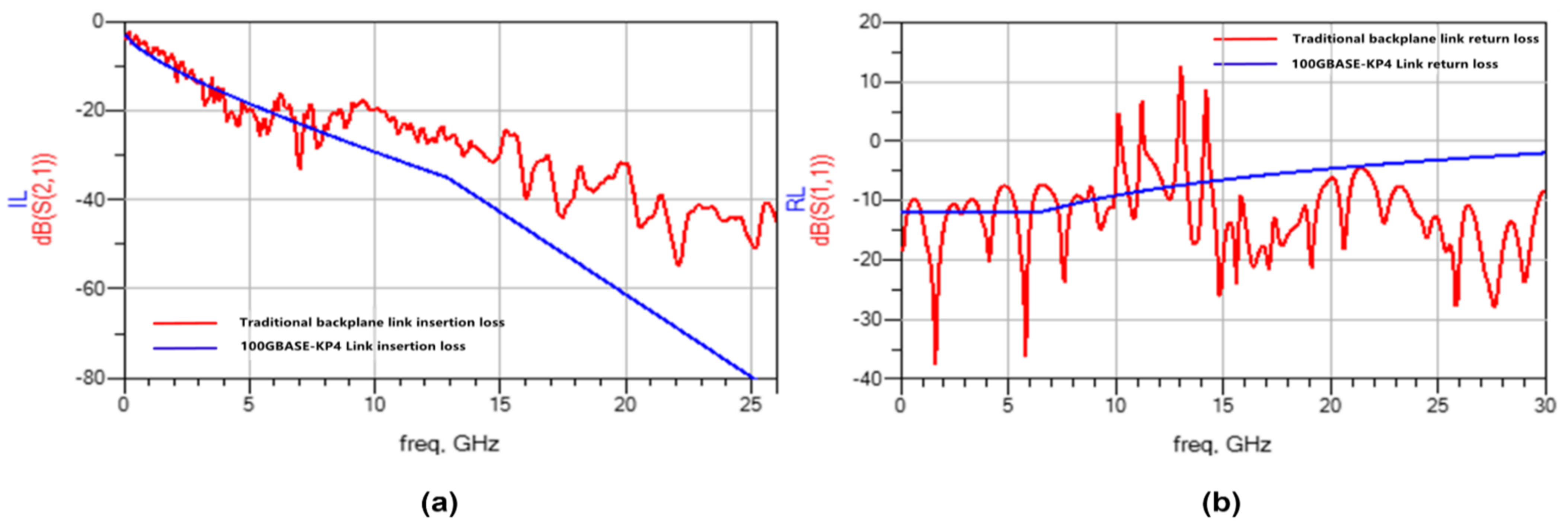
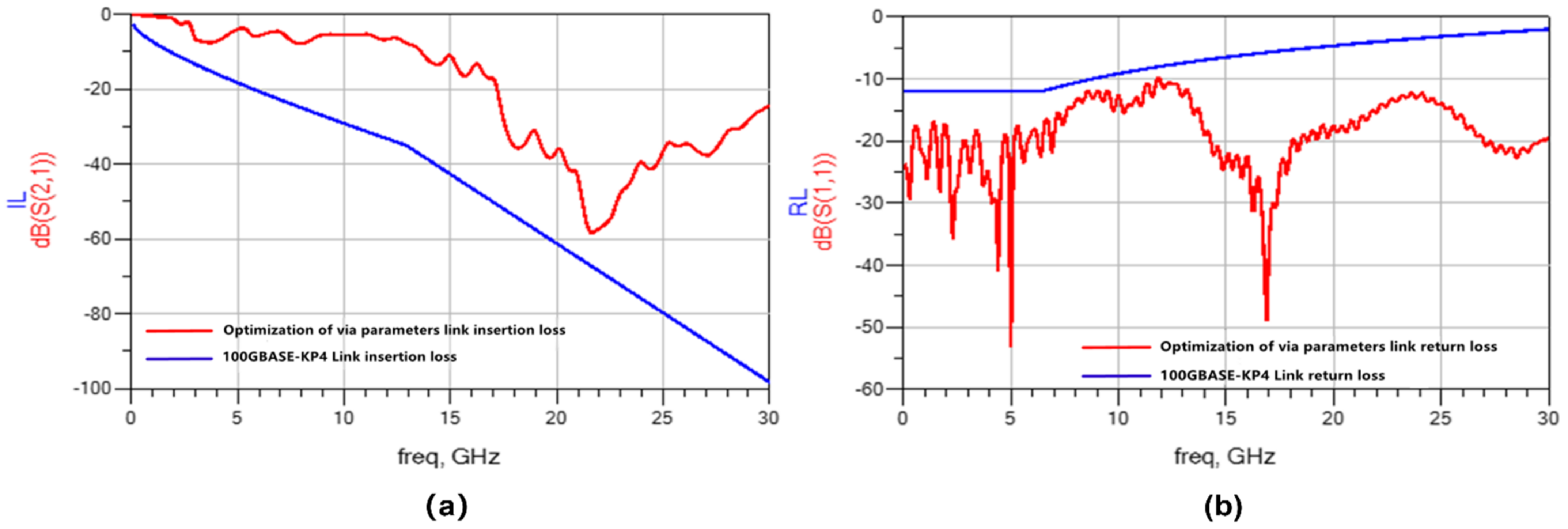
3.2. Simulation Results of Overall Optimization
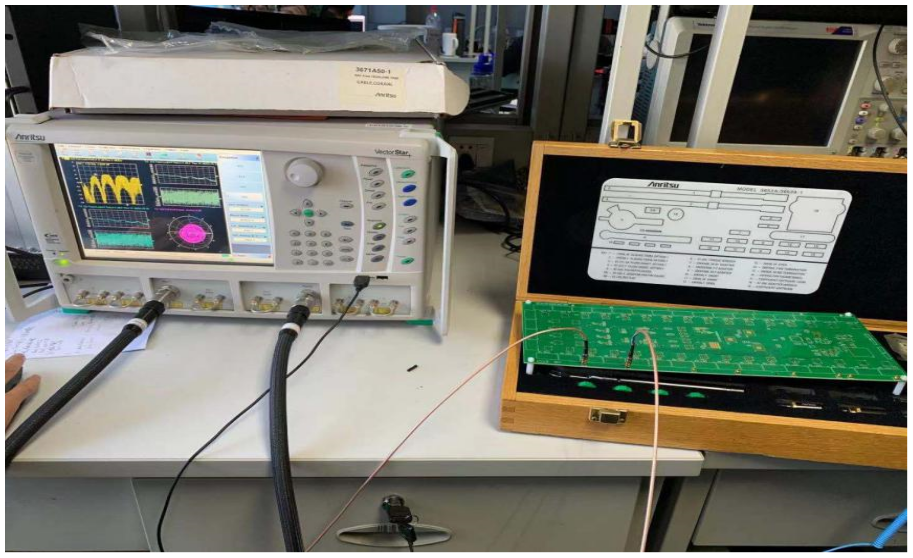
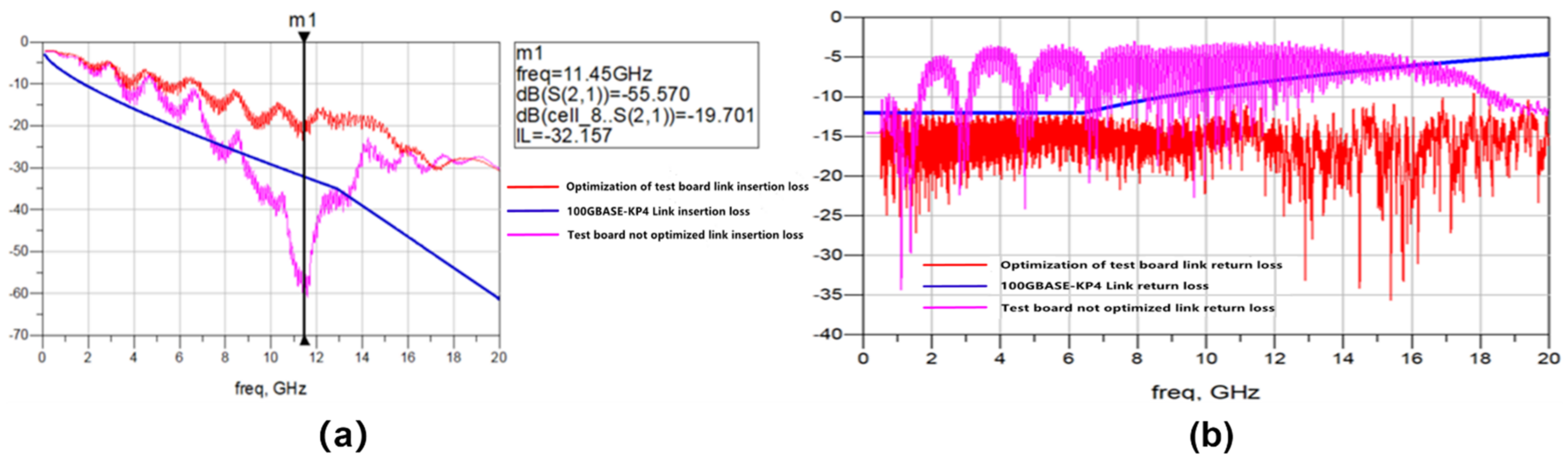
3.3. Backplane Passive Link Actual Test Results
4. Discussion
5. Conclusions
Author Contributions
Funding
Conflicts of Interest
References
- Gao, H. Design and Implementation of Interconnection Gateway between, Wantrillion Ethernet and Infiniband Network. Master’s Thesis, Nanjing University of Post and Telecommunications, Nanjing, China, 2016. [Google Scholar]
- Zhuo, Q. Research on Signal Integrity of USB3.0 Data Transmission System. Master’s Thesis, Harbin Engineering University, Harbin, China, 2016. [Google Scholar]
- Bokhari, S.; Ali, H. On grounded co-planar waveguides as interconnects for 10Gbp/s signals. In Proceedings of the IEEE International Symposium on Electromagnetic Compatibility, Boston, MA, USA, 18–22 August 2003; Volume 2, pp. 607–609. [Google Scholar]
- Yee, C.F.; Jambek, A.B.; Al-Hadi, A.A. Advantages and Challenges of 10-Gbps Transmission on High-Density Interconnect Boards. J. Electron. Mater. 2016, 45, 3134–3141. [Google Scholar] [CrossRef]
- Jiang, W. Signal Integrity Design of 25 Gbps Cross Backplane High Speed Serial Link. Master’s Thesis, Harbin Institute of Technology, Harbin, China, 2016. [Google Scholar]
- Zheng, Y. Research on Signal Integrity of 10 Gbps Cross Backplane High Speed Serial Link. Master’s Thesis, Shanghai Jiaotong University, Shanghai, China, 2017. [Google Scholar]
- Shi, H. Design of TCP/IP Offload Engine and Hardware System for 10 Gigabit Ethernet Based on FPGA. Master’s Thesis, East China Normal University, Shanghai, China, 2020. [Google Scholar]
- Yoon, S.J.; Jeong, S.H.; Yook, J.G. A novel CPW structure for high-speed interconnects. In Proceedings of the IEEE MTT-S International Microwave Symposium Digest, Phoenix, AZ, USA, 20–25 May 2001; Volume 2, pp. 771–774. [Google Scholar]
- Zhou, Z. 40gbase-kr4 transmission channel simulation and backplane design optimization. Commun. Technol. 2017, 50, 1564–1569. [Google Scholar]
- Zhou, D. Fast Analysis of Microwave Circuit by Time Domain Spectral Element. Master’s Thesis, Nanjing University of Technology, Nanjing, China, 2010. [Google Scholar]
- Wang, W. Discontinuous Galerkin Frequency-Domain Finite Element Analysis of Microwave Circuits. Master’s Thesis, Nanjing University of Science and Technology, Nanjing, China, 2013. [Google Scholar]
- Renyi, C. Signal Integrity Analysis and Optimization of High Speed PCB Transmission Path. Master’s Thesis, Jiangxi University of Technology, Ganzhou, China, 2020. [Google Scholar]
- Amleshi, P.; Shah, V.; Yang, Z.; Mohan, J.; Mukherjee, T. 25 Gbps backplane links frequency and time domain characterization—Correlation study between test and full-wave 3D EM simulation. In Proceedings of the IEEE International Symposium on Electromagnetic Compatibility, Long Beach, CA, USA, 14–19 August 2011; pp. 809–813. [Google Scholar]
- Yee, C.F.; Isa, M.M.; Al-Hadi, A.A.; Arshad, M.K. Techniques of impedance matching for minimal PCB channel loss at 40 GBPS signal transmission. Circuit World 2019, 45, 132–140. [Google Scholar] [CrossRef]
- Mahmud, M.Z.; Islam, M.T.; Misran, N.; Kibria, S.; Samsuzzaman, M. Microwave imaging for breast tumor detection using uniplanar AMC based CPW-fed microstrip antenna. IEEE Access 2018, 6, 44763–44775. [Google Scholar] [CrossRef]
- Du, J. High Density Microwave Signal Transmission and Control Technology Based on Multilayer Printed Circuit Board. Master’s Thesis, University of Electronic Science and Technology, Chengdu, China, 2018. [Google Scholar]
- Peng, Y. Research and Application of Planar Circuit Based on Coplanar Waveguide. Master’s Thesis, Nanjing University of Posts and Telecommunications, Nanjing, China, 2015. [Google Scholar]
- Zhao, S.; Withington, S.; Goldie, D.J.; Thomas, C.N. Electromagnetic models for multilayer superconducting transmission lines. Supercond. Sci. Technol. 2018, 31, 1–10. [Google Scholar] [CrossRef] [Green Version]
- Chen, E.; Chou, S.Y. Characteristics of coplanar transmission lines on multilayer substrates: Modeling and experiments. IEEE Trans. Microw. Theory Tech. 1997, 45, 939–945. [Google Scholar] [CrossRef] [Green Version]
- Eisenstadt, W.R.; Eo, Y. S-parameter-based IC interconnect transmission line characterization. IEEE Trans. Comp. Hybrids Manuf. Technol. 1992, 1, 483–490. [Google Scholar] [CrossRef]
- Sejas, S.; Torres, R.; Murphy, R. Modeling transmission lines on silicon in frequency- and time-domains from S-parameters. IEEE Trans. Electron Devices 2012, 59, 1803–1806. [Google Scholar] [CrossRef]
- Tang, J. Research on Simplification of EMC Simulation Model of Electronic Equipment. Master’s Thesis, Xidian University, Xi’an, China, 2008. [Google Scholar]
- Zhang, J.; Lim, J.; Yao, W.; Qiu, K.; Brooks, R. PCB via to trace return loss optimization for >25 Gbps serial links. In Proceedings of the 2014 IEEE International Symposium on Electromagnetic Compatibility, Gaithersburg, MD, USA, 4–8 August 2014; pp. 619–624. [Google Scholar]
- Dong, G.; Biao, Y.; Xidong, D.; Yuan, L. Research on the influence of vias on signal transmission in multi-layer PCB. In Proceedings of the 2017 13th IEEE International Conference on Electronic Measurement & Instruments (ICEMI), Yangzhou, China, 20–23 October 2017; pp. 406–409. [Google Scholar]
- Kok, P.; Zutter, D.D. Capacitance of a circular symmetric model of a via hole including finite ground plane thickness. IEEE Trans. Microw. Theory Tech. 1991, 39, 1229–1234. [Google Scholar] [CrossRef]
- Kok, P.A.; De Zutter, D. Prediction of the excess capacitance of a via-hole through a multilayered board including the effect of connecting microstrips or striplines. IEEE Trans. Microw. Theory Tech. 1994, 42, 2270–2276. [Google Scholar] [CrossRef]
- Oh, K.S.; Schutt-Aine, J.E.; Mittra, R.; Wang, B. Computation of the equivalent capacitance of a via in multilayered board using the closed-form Green’s function. IEEE Trans. Microw. Theory Tech. 1996, 44, 347–349. [Google Scholar] [CrossRef]
- Mathis, A.W.; Peterson, A.F.; Butler, C.M. Rigorous and simplified models for the capacitance of a circularly synmetric via. IEEE Trans. Microw. Theory Tech. 1997, 45, 1875–1878. [Google Scholar] [CrossRef]
- Tan, Y. Microwave Engineering, 4th ed.; Electronic Industry Press: Beijing, China, 2019. [Google Scholar]
- Zhao, X. Research on Transmission Characteristics and Impedance Matching of Vertical Silicon via Signal Channel. Master’s Thesis, Xidian University, Xi’an, China, 2017. [Google Scholar]
- Li, D. Research on High Precision Antenna of Satellite Navigation System and Its Multipath Suppression Technology. Master’s Thesis, University of National Defense Science and Technology, Beijing, China, 2017. [Google Scholar]
- TE Connectivity (TE). Available online: https://www.te.com.cn/chn-zh/products/connectors/pcb-connectors/backplane-connectors/high-speed-backplane-connectors/strada-whisper.html?tab=pgp-story (accessed on 22 June 2021).
- Li, K. How to verify the performance of 100 g backplane. Appl. Electron. Technol. 2015, 41, 9–11. [Google Scholar]
- Yang, A. Design and Evaluation Method Based on High Speed Hybrid Backplane. Master’s Thesis, University of Defense Science and Technology, Beijing, China, 2017. [Google Scholar]
- Wang, Z. Research on PCI Express Transmission Link Design and Si Simulation Technology Based on Backplane System. Master’s Thesis, National Defense Science and Technology, Beijing, China, 2012. [Google Scholar]


Publisher’s Note: MDPI stays neutral with regard to jurisdictional claims in published maps and institutional affiliations. |
© 2021 by the authors. Licensee MDPI, Basel, Switzerland. This article is an open access article distributed under the terms and conditions of the Creative Commons Attribution (CC BY) license (https://creativecommons.org/licenses/by/4.0/).
Share and Cite
Liu, J.; Zhang, K.; Wu, Q.; Peng, L.; Yao, K.; Liu, H. Optimization and Design of Passive Link with Single Channel 25 Gbps Based on High-Speed Backplane. Electronics 2021, 10, 1773. https://doi.org/10.3390/electronics10151773
Liu J, Zhang K, Wu Q, Peng L, Yao K, Liu H. Optimization and Design of Passive Link with Single Channel 25 Gbps Based on High-Speed Backplane. Electronics. 2021; 10(15):1773. https://doi.org/10.3390/electronics10151773
Chicago/Turabian StyleLiu, Jie, Kai Zhang, Qiang Wu, Li Peng, Kai Yao, and Hu Liu. 2021. "Optimization and Design of Passive Link with Single Channel 25 Gbps Based on High-Speed Backplane" Electronics 10, no. 15: 1773. https://doi.org/10.3390/electronics10151773
APA StyleLiu, J., Zhang, K., Wu, Q., Peng, L., Yao, K., & Liu, H. (2021). Optimization and Design of Passive Link with Single Channel 25 Gbps Based on High-Speed Backplane. Electronics, 10(15), 1773. https://doi.org/10.3390/electronics10151773