Review

Evaluation of Low-Frequency Noise in MOSFETs Used as a Key Component in Semiconductor Memory Devices

Research Institute for Nanodevice and Bio Systems, Hiroshima University, Higashi-Hiroshima 739-8527, Japan
Electronics 2021, 10(15), 1759; https://doi.org/10.3390/electronics10151759
Submission received: 22 June 2021 / Revised: 15 July 2021 / Accepted: 20 July 2021 / Published: 22 July 2021
(This article belongs to the Special Issue High-Density Solid-State Memory Devices and Technologies)

Abstract

:
Methods for evaluating low-frequency noise, such as 1/f noise and random telegraph noise, and evaluation results are described. Variability and fluctuation are critical in miniaturized semiconductor devices because signal voltage must be reduced in such devices. Especially, the signal voltage in multi-bit memories must be small. One of the most serious issues in metal-oxide-semiconductor field-effect-transistors (MOSFETs) is low-frequency noise, which occurs when the signal current flows at the interface of different materials, such as SiO2/Si. Variability of low-frequency noise increases with MOSFET shrinkage. To assess the effect of this noise on MOSFETs, we must first understand their characteristics statistically, and then, sufficient samples must be accurately evaluated in a short period. This study compares statistical evaluation methods of low-frequency noise to the trend of conventional evaluation methods, and this study’s findings are presented.

1. Introduction

Semiconductor devices have been basically progressed with the shrinking of MOSFETs (metal-oxide-semiconductor field-effect-transistors), which are used as the key component in them. The shrinkage has been performed following the rule of the constant electric field in MOSFETs, which decreases signal voltage [1,2]. In addition, power consumption of electronic devices has skyrocketed because the amount of digital data generated is growing at a rate faster than Moor’s law [3,4]. The reduction of power consumption strongly requires decreasing supply voltage of MOSFETs because power consumption (P) is proportional to the square of the supply voltage (Vdd) as follows [5].
P = C L V dd 2 f
where CL represents the load capacitor and f represents the switching frequency of the circuit. The growth of clock frequency in the leading edge logic devices has stopped by exceeding the heat extraction capability. However, the downscaling has been continued to reduce the cost. In the other devices, the downscaling the device size has also been continued to reduce the power consumption and the other reasons. As a result, as the device size is reduced, the signal voltage of MOSFETs decreases. Memory devices’ power consumption and supply voltage also have to be reduced [6,7,8,9] because of the same reasons as the logic devices and reducing a leakage current. On the other hand, a decrease in signal voltage degrades the reliability of electronic circuits, including analog and digital devices.
The logic (bit) error rate (LER) is given by the following equation.
LER = P 0 α f 0 ( x ) dx + P 1 α f 1 ( x ) dx
where P0 and P1 represent the probabilities of signals “0” and “1”, respectively, α represents the identification level between “0” and “1”, and f0(x) and f1(x) represent noise amplitude densities superimposed on “0” and “1”, respectively. If f0 and f1 are Gaussian noise, the following equations apply.
f 0 ( x ) = 1 2 π σ 2 e x 2 2 σ 2 ,   f 1 ( x ) = 1 2 π σ 2 e ( x A S ) 2 2 σ 2
where AS represents the signal amplitude and σ represents the standard deviation of the noise. When P0 = P1 = 1/2 and α = AS/2 are assumed, the LER is given by the following equation from Equations (2) and (3).
LER = 1 2 erfc ( A S 2 2 σ 2 )
erfc ( x ) = 1 erf ( x ) = 1 2 π 0 x e t 2 dt = 2 π x e t 2 dt
When Nyquist transmission rate is the same as the signal band, the signal to noise (S/N) ratio (dB) is given by the following equation.
S N = E b N 0 = 20 log ( A S σ )
where Eb and N0 represent signal and noise energy per second, respectively. From Equations (4) and (6), the LER is given by the S/N ratio as follows [10].
LER = 1 2 erfc { 1 2 2 10 1 20 ( S N ) }
Figure 1 shows the LER as a function of S/N (dB) and A/σ ratios [10]. The LER decreases with an increase in S/N (AS/σ) ratio. On the other hand, to guarantee that a system does not make a mistake even once during the operation period, the LER should be reduced as shown in the following equation.
LER 1 N L × F × T
where NL, F, and T represent the number of logic gates in a chip, the number of operations per second, and the guarantee period, respectively. For example, the LER should be less than 3 × 10⁻²⁶ for a circuit with 108 logic gates, 109 Hz operations, and a 10-year (3 × 10⁸ s) operation period, and then the S/N (AS/σ) ratio should be greater than 26.5 dB (21.1).
For example, we consider signal electrons required from a no error operation. Figure 2 shows (a) Variation in the number of electrons as a function of the number of signal electrons. (b) Logic error rate as a function of the number of signal electrons. When a signal is constructed by a constant number of electrons (Ne), the standard deviation of the number of electrons is (Ne)1/2, and then the A/σ ratio is (Ne)1/2. As a result, the number of electrons must be greater than 445 to maintain an S/N (AS/σ) ratio of 26.5 dB (21.1). If the number of signal electrons is 1, the LER must be equal to 0.3. Then, such a system produces the wrong output once every three calculations.
The electronic circuit will be influenced by noise, such as thermal noise, quantum noise, and flicker noise. The noise voltage (vnf) in 1/f noise is defined by the following equation.
v nf = K F C OX × L × W ln ( f H f L )
where KF represents the flicker noise coefficient, fL~fH is the frequency period for device operation, COX, L, and W represent the gate oxide capacitance, gate length, and gate width of a MOSFET, respectively. Noise increases with device shrinkage because vnf is inversely proportional to C OX LW [11,12,13,14]. It has been pointed out that 1/f noise may influence not only analog devices, but also digital devices when device shrinkage and the decreasing signal voltage are moved on [15]. Random telegraph noise (RTN), another low-frequency noise also affects electronic devices, such as CMOS image sensor [16,17,18,19,20,21], static random access memory (SRAM) [22,23,24,25], dynamic random access memory (DRAM) [25], and flash memory [26,27,28,29,30,31,32]. Low-frequency noise, such as 1/f noise and RTN, have high variability [33,34] because they must be statistical phenomena by nature, and statistical analysis is required to fully understand this phenomenon. The conventional evaluations of the noise in MOSFETs have performed with a few sample numbers, and then we could understand only typical noise characteristics of MOSFETs having relatively large noise. However, we need statistical information of the noise for the design of LSI. Then, low-frequency noise statistical evaluation methods and evaluation results are described in this study.

2. Evaluation Methods

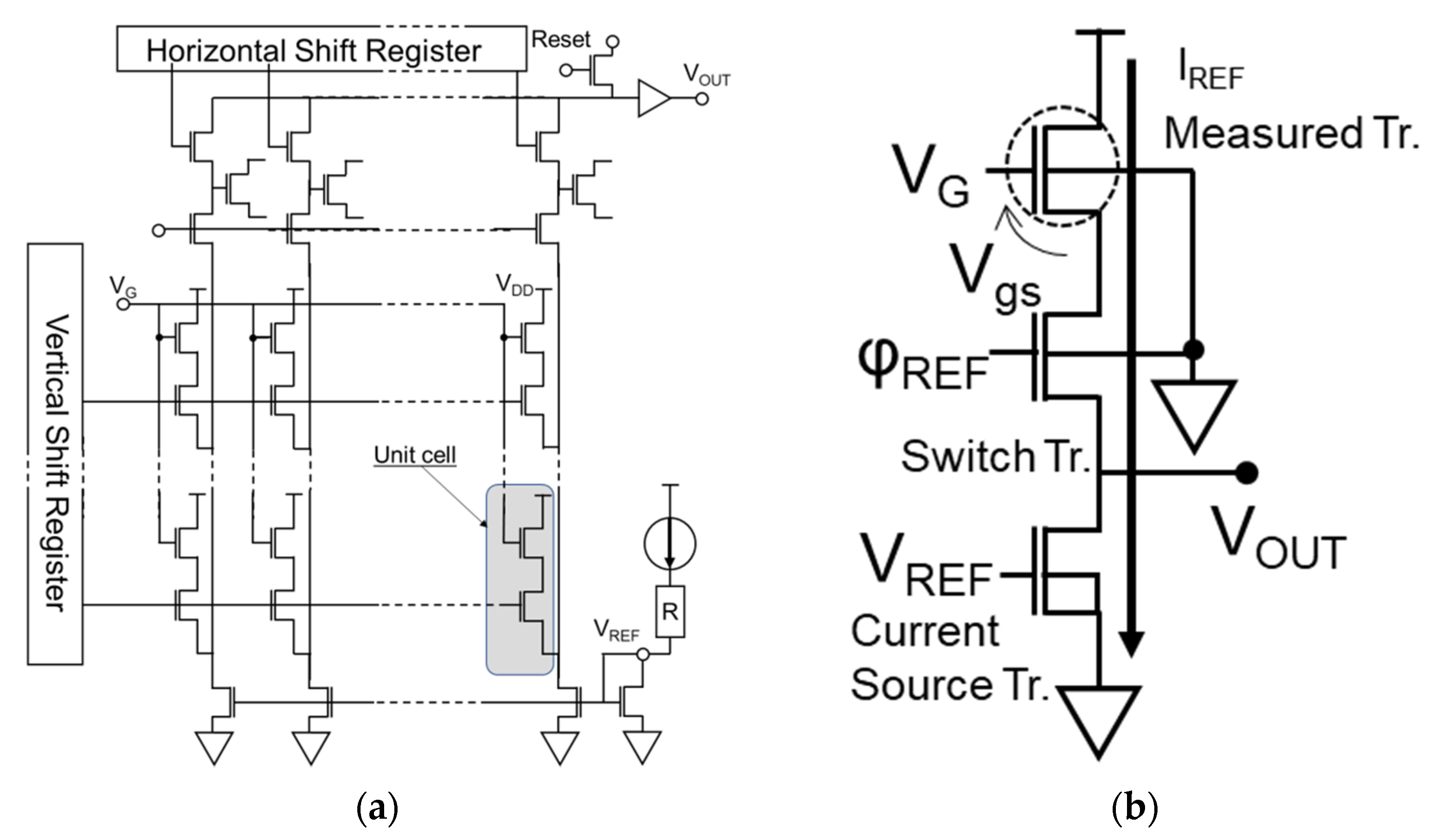
2.1. Test Pattern for Noise Evaluation

The test structure is constructed using 0.22 μm, 1-poly 2-metal standard CMOS technology and includes n-MOSFETs of various gate sizes [35,36,37,38] as shown in Table 1. The measured MOSFETs are arrayed in 1024 rows and 1776 columns (total number of MOSFETs: 1217856) in a chip at 5 μm intervals. The size of the MOSFETs, and their number, and location in a chip are shown in Table 1. The test chip has an area of 5.5 mm × 14 mm. The gate insulator is formed by pyrogenic oxidation and is 5.8 nm thick.
A schematic block diagram of a test pattern is shown in Figure 3a [35,37,39,40]. This is composed of MOSFETs measured in arrayed unit cells, vertical and horizontal shift registers for addressing measured MOSFETs, MOSFETs located on each column for current control of measured MOSFET, analog memories for storing the source voltage of the measured MOSFETs within one line, and a source follower circuit for amplifying the output signal. The drain (VD) and gate (VG) voltage in measured MOSFETs and the gate voltage applied to current source MOSFETs (VREF) are supplied from the external voltage source simultaneously. VDD and VSS are the supply voltages in the peripheral circuits and ground voltage, respectively. The measured MOSFET and current source transistor construct a source follower circuit using a select transistor. This test structure uses simple peripheral circuits. Therefore, it can be used to evaluate various MOSFETs with varying gate lengths, gate widths, gate insulator films, thicknesses, and other characteristics. Figure 3b shows the circuit schematic of a unit cell and current source transistor in Figure 1, which is the principle of this measurement. A unit cell is constructed with a measured MOSFET and a select transistor. When the current source transistor operates at a saturation region, IREF is independent of the voltage between the source and drain in the current source transistor (Vout). When the gate bias of the select transistor (Φx) is applied from a vertical shift register, IREF flows into the measured MOSFET. The output voltage (Vout) is indicated as follows.
V gs = V G V out I REF · R select V G V out
where Rselect is the channel resistance of the select switch transistor. The select transistor must be operated in the linear region to have sufficient high channel conductivity compared with the measured MOSFET, and then, IREF∙Rselect can be neglected. The output signal can be obtained as a source voltage for each measured MOSFET by shift register scanning, and then 1.2 million MOSFETs can be measured within approximately 0.7 s. The electrical characteristics of the measured MOSFETs can be observed as the Vgs included in the output voltage Vout (Figure 3b). In this frame measurement mode, each MOSFET can be measured every 0.7 s. This test pattern has another measurement mode, which can measure a specific MOSFET every 1 μs.

2.2. Extraction of Amplitude and Time Constant of RTN

Two-level type RTN is characterized by only three parameters, which are the mean time to capture (<τc>), mean time to emission (<τe>), and amplitude (ΔVgs). The time constants correspond to two physical states of a trap, that is, τc and τe represent spans in a low Vgs level (carrier trapping state) and high Vgs level (carrier emission state), respectively (Figure 4a). The RTN amplitude ΔVgs is defined as the difference between two normal distributions in a voltage histogram (Figure 4b). We extract the time constants by fitting the distributions of τc and τe to the exponential distribution (Ae−t/<τ>) because the phenomenon is governed by the Poisson process. The time constants can be extracted with μs accuracy using the specific MOSFET measurement mode.
The time constant ratio <τe>/<τc> is also an important parameter in RTN because the energy level of a trap that causes RTN is related to the constant ratio as follows [12,41,42,43].
< τ c > < τ e > = gexp ( E T E F kT )
where ET and EF represent the energy of the trap and Fermi energy of the channel, respectively; k, T, and g represent Boltzmann constant, temperature, and degeneracy factor, respectively, where g is assumed to 1. Then, the energy of the trap level is indicated by (12).
E T E F = kTln ( < τ c > < τ e > )
We can use the frame measurement mode to extract the time constant ratio, and the 1.2 million MOSFETs can be measured 10,000 times in 7000 s (sampling period = 0.7 s). An average of the time constant ratio <τe>/<τc> is the same as Count-L/Count-H (shown in Figure 4b), where Count-L and count-H are the numbers of low and high states, respectively [41,42,43,44]. When the time constant is greater than a sampling frequency of 0.7 s, the detected number of transition times is the same as the transition time of RTS characteristics. However, when the time constant is less than 0.7 s, the detected number of transition times is less than the real one; however, it is proportional to the real one because the absolute value of the time constant, which is less than the sampling frequency, cannot be extracted in this measurement. Then, the number of transition times is defined as the detected ones in the sampling frequency of 0.7 s.

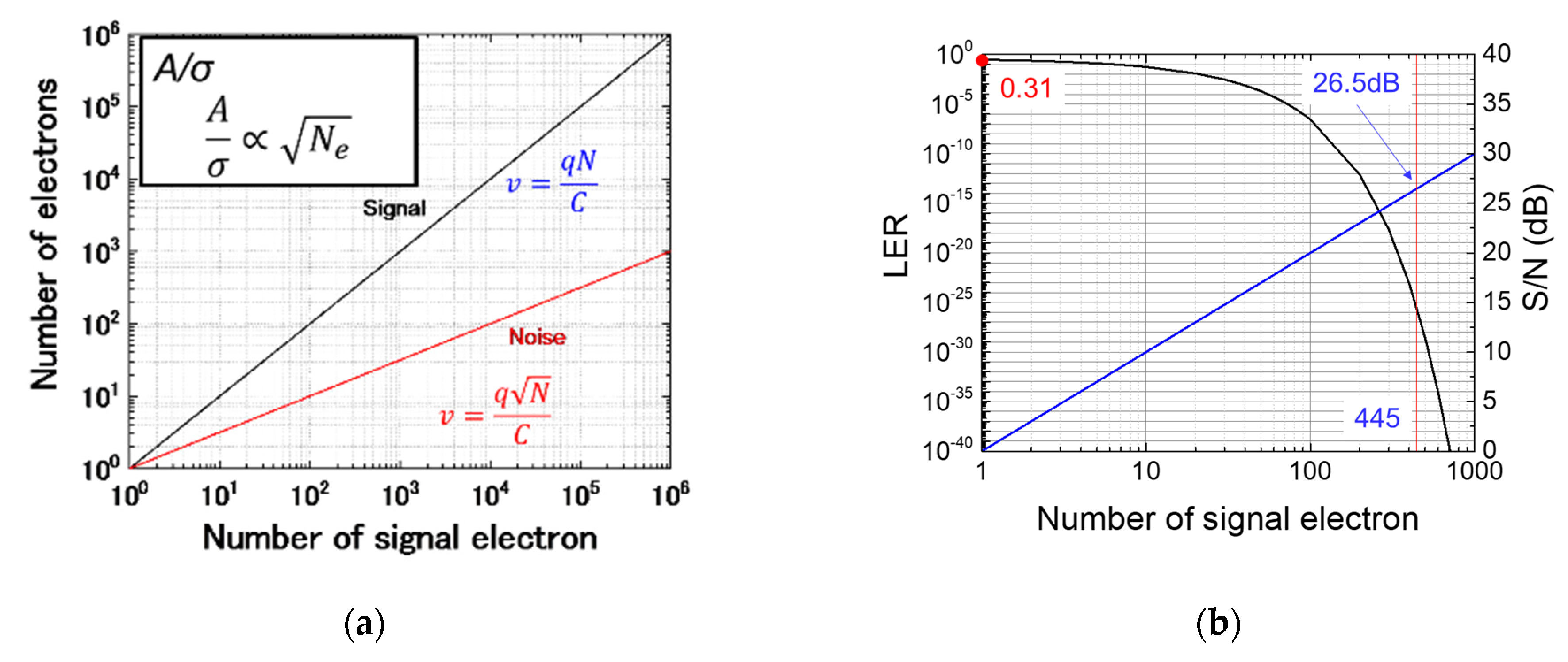
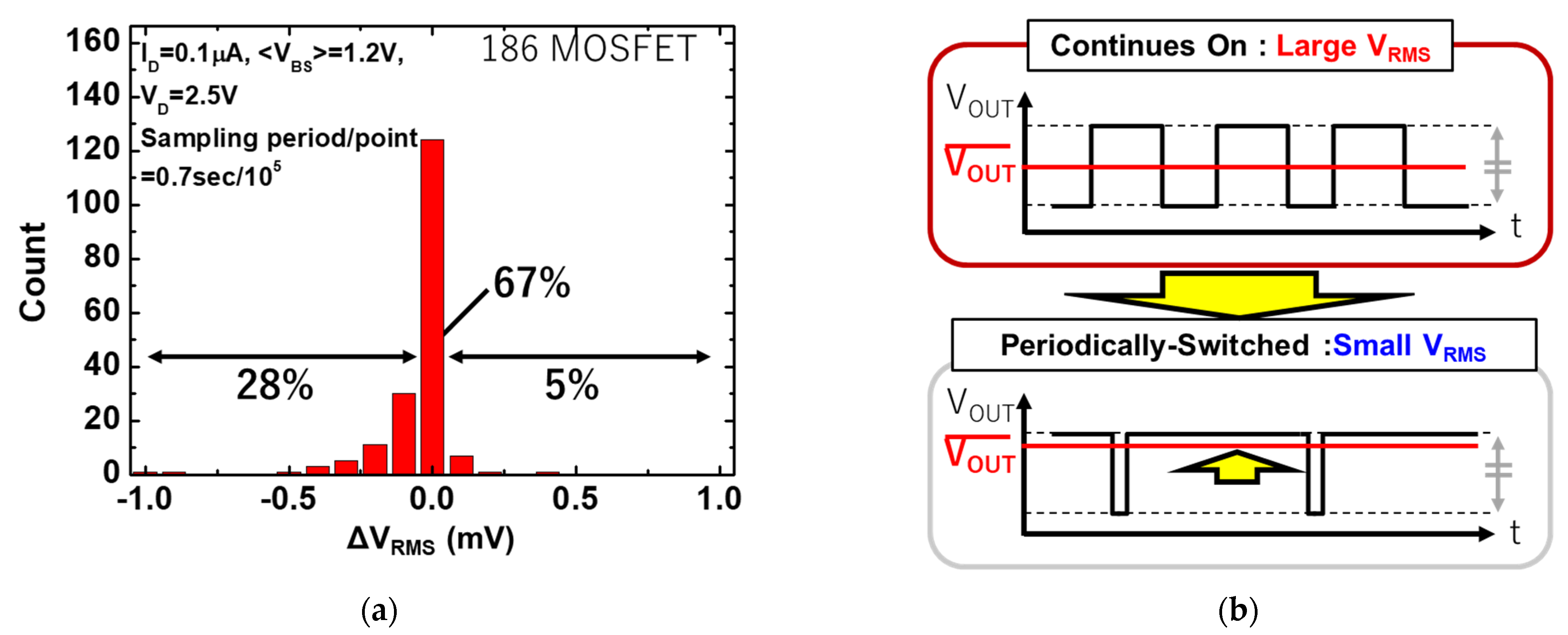
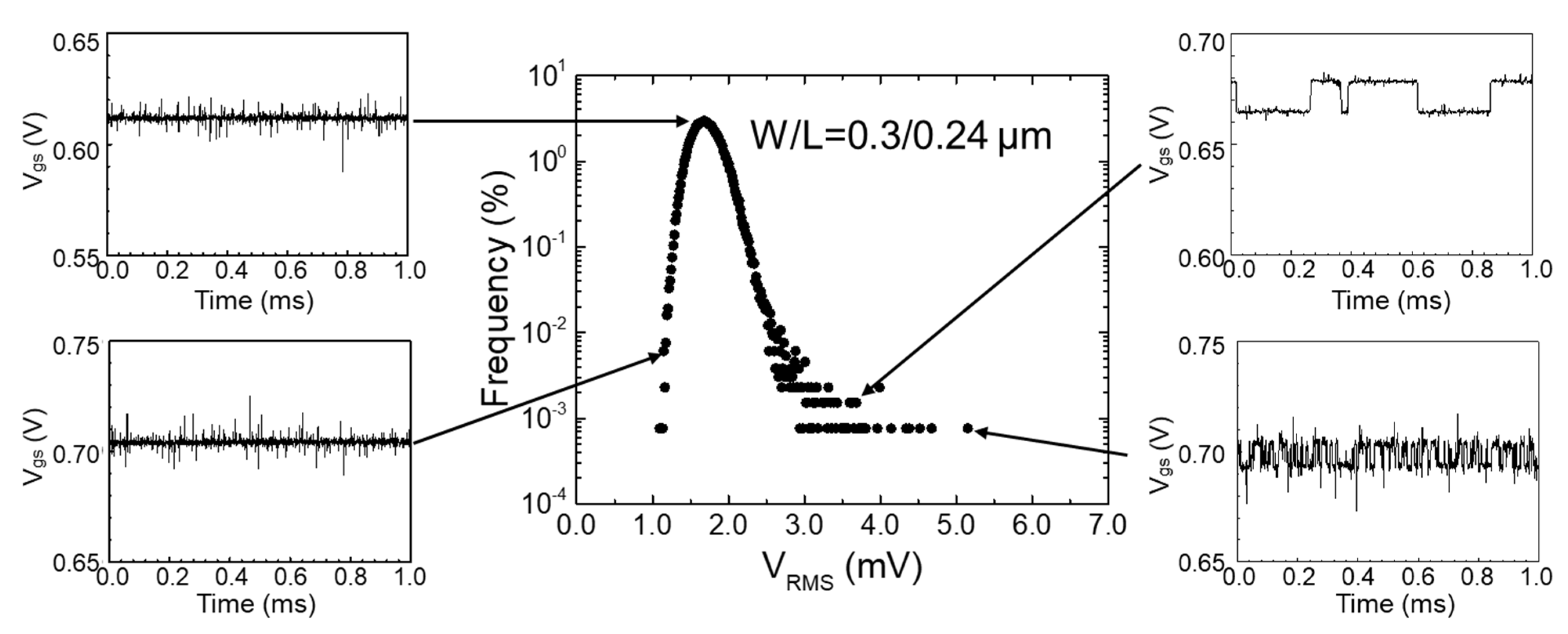
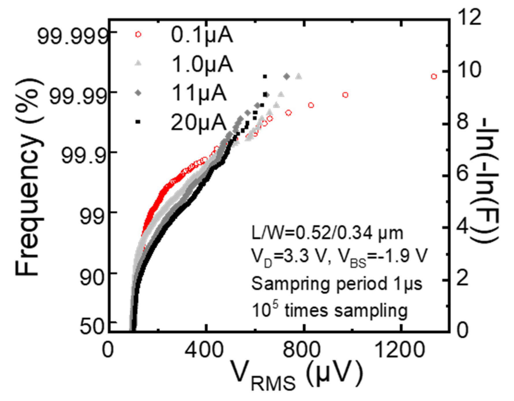
2.3. Root Mean Square of RTN Waveform

The root mean square (RMS) of the signal waveform is often used for the representative parameter of noise [45], and the RMS of the output voltage VRMS is defined as follows in this study.
V RMS = i = 1 N ( V out , i V out ¯ ) 2 N 1 = A < τ e > < τ c > < τ e > + < τ c >
where V out , i , V out ¯ , N, and A are the output voltage at ith sampling, average of V out , sampling numbers, and the amplitude of two-state RTN, respectively. Using VRMS, we can obtain MOSFETs with high noise from many measured MOSFETs. Figure 5 shows the relationship between VRMS and RTN waveform. The waveform with large RTN corresponds to large VRMS.

3. Results and Discussion

3.1. Statistical Evaluation of RTN Characteristics

The 1/f noise increases with downscaling of MOSFETs, as mentioned above, and RTN also increase with the downscaling [12,36,37]. Figure 6 shows the Gumbel plot of VRMS for the various MOSFET sizes [36,37]. A large VRMS can be observed in small-size MOSFETs (L/W = 0.22/0.28, 0.22/0.3, 0.24/0.3 μm). In this experiment, noise cannot be observed in large MOSFETs because the floor noise is relatively high at ~2.5 mV.
Figure 7a shows the Gumbel plot of VRMS for the various IDS varied from 0.13 to 12.7 μA. The sizes of MOSFETs are L/W = 0.22/0.28 μm and VBS = −1.0 V [39]. The data in (a) and (b) were measured by the frame and specific MOSFET measurement modes, respectively. The number of MOSFETs with large noise increases with decreasing IDS, which is controlled by Vgs. This means that the event probability of large noise increases with decreasing Vgs because the number of channel electrons decreases with decreasing Vgs, and then the effect of a trapped electron charge becomes large with decreasing number of channel electrons. The number of channel electrons also decreases with the shrinkage of transistor size shown in Figure 6, and then, the probability increases with decreasing channel size. Figure 7b shows the waveform of typical MOSFETs for IDS of 0.13, 0.38, and 1.3 μA [39]. The time constants and amplitude are modulated by IDS. With increasing IDS (Vgs), amplitude and τc decrease, whereas τe slightly increases. An increase in Vgs decreases ET-EF, and then, the time to capture decreases as shown in Equation (11). The difference between the modulation of τe and τc is discussed later. The modulation of amplitude is caused by a decrease in the number of electrons, as discussed above. It is considered that decreasing the time to capture and increasing amplitude with decreasing Vgs increases the event probability of large noise. Figure 8a shows the Gumbel plot of VRMS for the various back bias (VBS). VBS varied from −0.075 to −1.38 V, and Figure 8b shows the waveform of typical MOSFETs for VBS of 0.6 1.0 and 1.3 V [39]. The probability increases with the absolute value of VBS in (a). In this experiment, IDS was constant at 1.0 μA, and this means that the number of electrons was almost the same for each VBS. Increasing VBS caused channel percolation [46,47,48,49], making the channel thickness narrow and percolated and increasing electron energy [50]. The probability is increased by channel percolation [46,47], and the varying electron energy modulates the time constants. In MOSFETs with RTN, the amplitude does not increase with increasing VBS because the number of electrons is the same for each VBS. This means that channel percolation increases the probability of RTN generation.
Figure 9 shows the Gumbel plot of the RTN amplitude for MOSFETs with varying channel doping [51]. The channel percolation is accelerated by increasing channel doping concentration [46,47,48]. This figure shows that the probability of the number of MOSFETs with large amplitude increases with doping concentration. RTN is increased by channel doping as well as doping the concentration near the source and drain regions. Figure 10 shows the Gumbel plot of VRMS for various Halo implantation concentrations [52]. The number of MOSFETs with large RTN increases with an increase in Halo implantation concentration. This indicates that the high dose in the channel region or near the source/drain region results in high RTN because of channel percolation enhancement.
Figure 11 shows the energy band diagrams and energy distribution of traps causing RTN for Vgs of 0.57, 0.53, and 0.46 V, respectively [41,42]. The difference between ET and EF for electrons is calculated using Equation (11). The blue shading and red solid bars in Figure 11 show the energy distribution of traps causing RTN in each measurement condition and common traps in all conditions, respectively. Although the shape of the distribution of each Vgs is almost the same, and the energy of common traps in all Vgs increases with decreasing Vgs. The conduction band edge (EC), the bottom sub-band energy (Esub), and 2nd sub-band energy (E2nd) in the inversion layer and EF are indicated in Figure 11 [50]. The energy levels of sub-bands were calculated using Equation (14) [50].
E j = [ 3 hqE s 4 2 m x ( j + 3 4 ) ] 2 3 ,   j = 0 , 1 ,
where Es is the electric field, h and mx represent Planck’s constant and effective mass of electrons, respectively. Ej is jth sub-band energy, and Esub and E2nd represent E0 and E1, respectively. The main energy distribution for each Vgs locates higher energy than the conduction band edge. It is considered that the energy level of traps is widely distributed, and the energy of the detected traps is determined by the electron energy in Esub and E2nd. Conversely, the energy of common traps in all Vgs increases with decreasing Vgs because the influence of trap energy on Vgs is larger than that of electron energy in the channel.

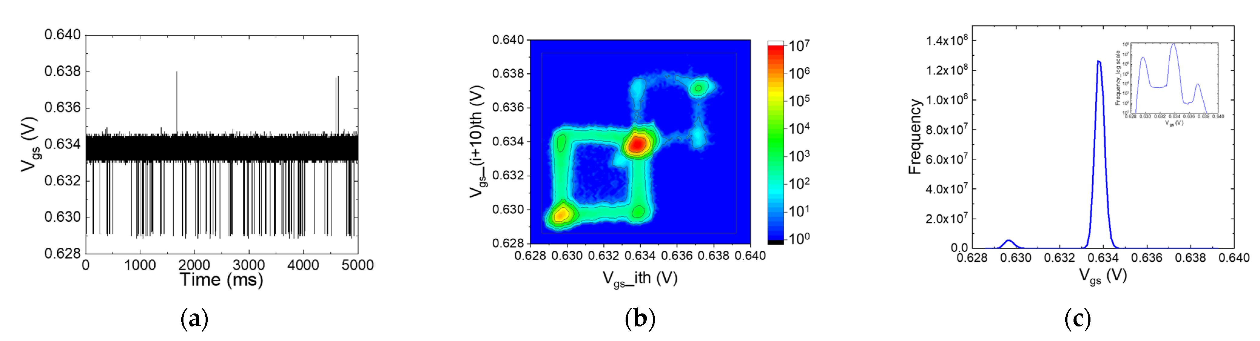
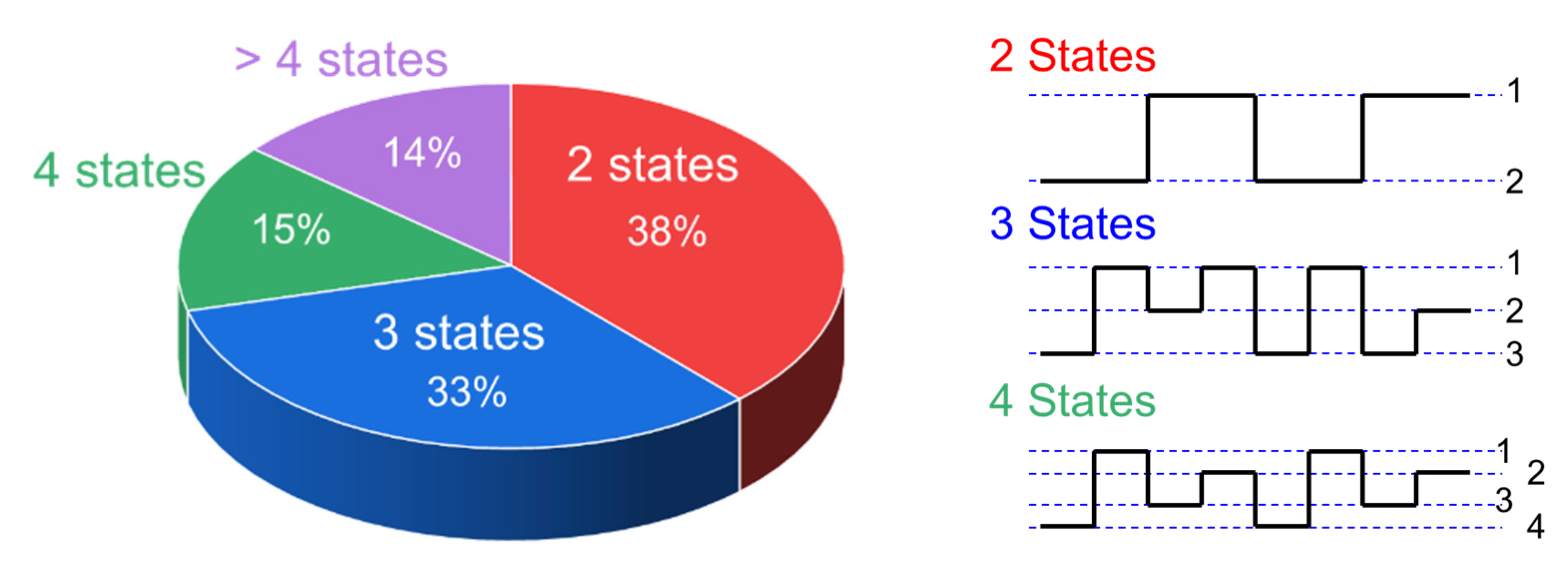
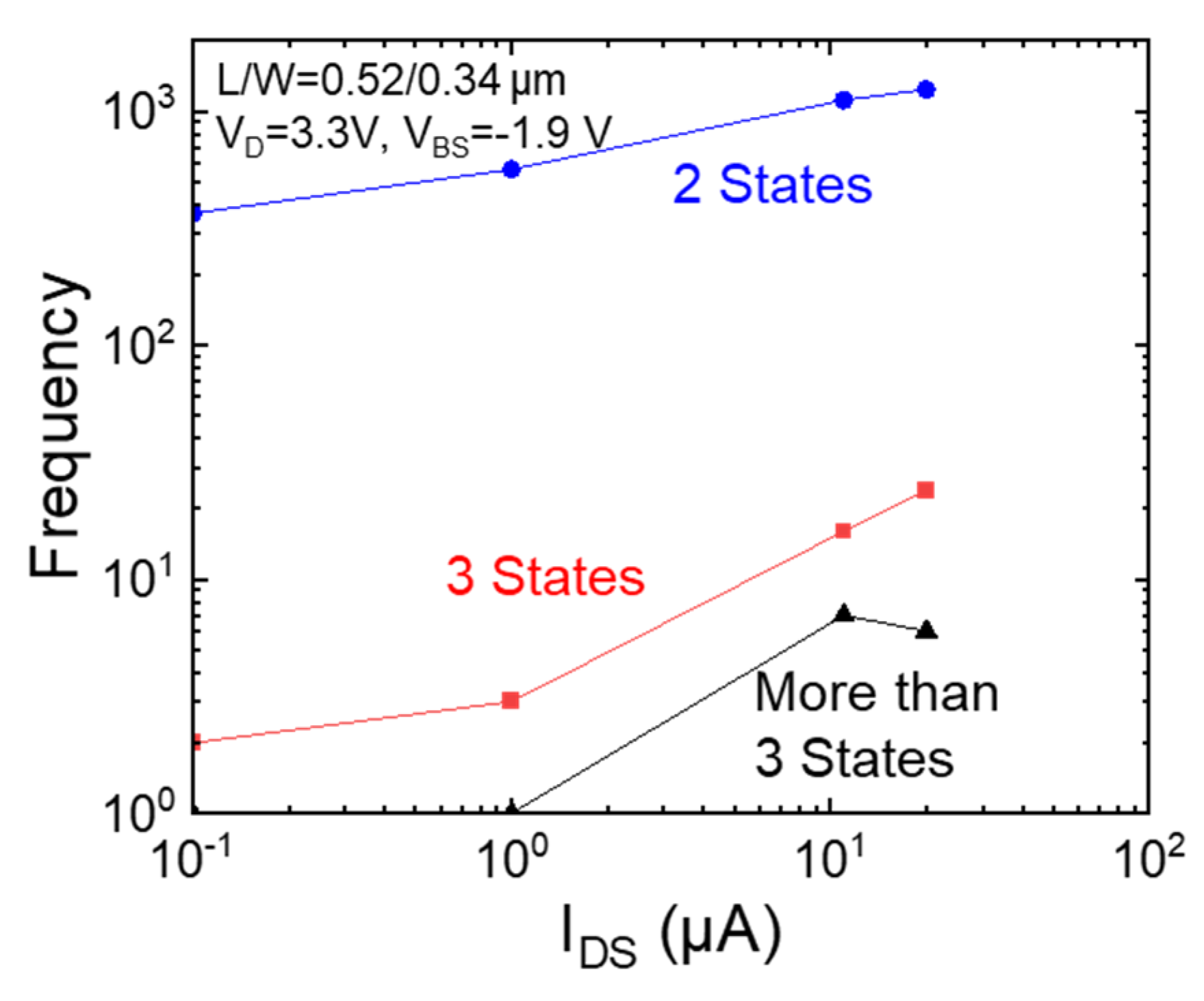
3.2. Multi-State RTN

Large VRMS RTN includes both two-state and multi-state RTN [34,53,54,55,56], which is considered to be generated by multi-traps. The analysis of trap characteristics, such as time constants and amplitude, in multi-state RTN is more difficult than that of two-state. Figure 12 shows the appearance probability of RTN with two, three, four, and more than four states. A large RTN (VRMS > 680 μV) was obtained by a frame measurement mode of the sampling period of 0.7 s/frame in IDS = 1 μA. 131,072 MOSFETs (L/W = 0.22/0.28 μm) were measured, and 2575 MOSFETs with large VRMS can be extracted. Then, we selected MOSFETs with large RTN and measured them by a specific measurement mode of a sampling period of 1 μs and a long sampling time of 10 min (sampling points = 6 × 10⁸) for the same bias condition [57,58]. Figure 13, Figure 14 and Figure 15 show the (a) waveform, (b) time lag plot (TLP), and (c) histogram for typical three-, four-, and six-state RTN. The number of peaks and the transition of each state can be understood via TLP [53,54,56].
Figure 13, Figure 14 and Figure 15 show the (a) waveform, (b) time lag plot (TLP), and (c) histogram for typical three-, four-, and six-state RTN. The number of peaks and the transition of each state can be understood via TLP [53,54,56]. Figure 13, Figure 14 and Figure 15b show the relationship of ith and (i + 10)th Vgs for the constant IDS. As shown in Figure 13b, transitions occur not from the lowest state to the highest state, but only via the medium state. When the trapping probability of some traps is even, the number of states should be even, and the transition from one position to the next can occur. To begin with, an odd number of states implies that the trapping probability for each trap is not independent of each other. A similar transition phenomenon occurs even in a four-state case. As shown in Figure 14b, transitions did not occur from the lowest state to the highest state or from the second-lowest state to the second-highest state. This also means that there are more than two traps, and the probability of trapping for each trap is not independent of each other. The characteristics of multi-trap RTN can be understood via TLP and waveforms [56]; however, these analyses become more difficult as the number of states increases.

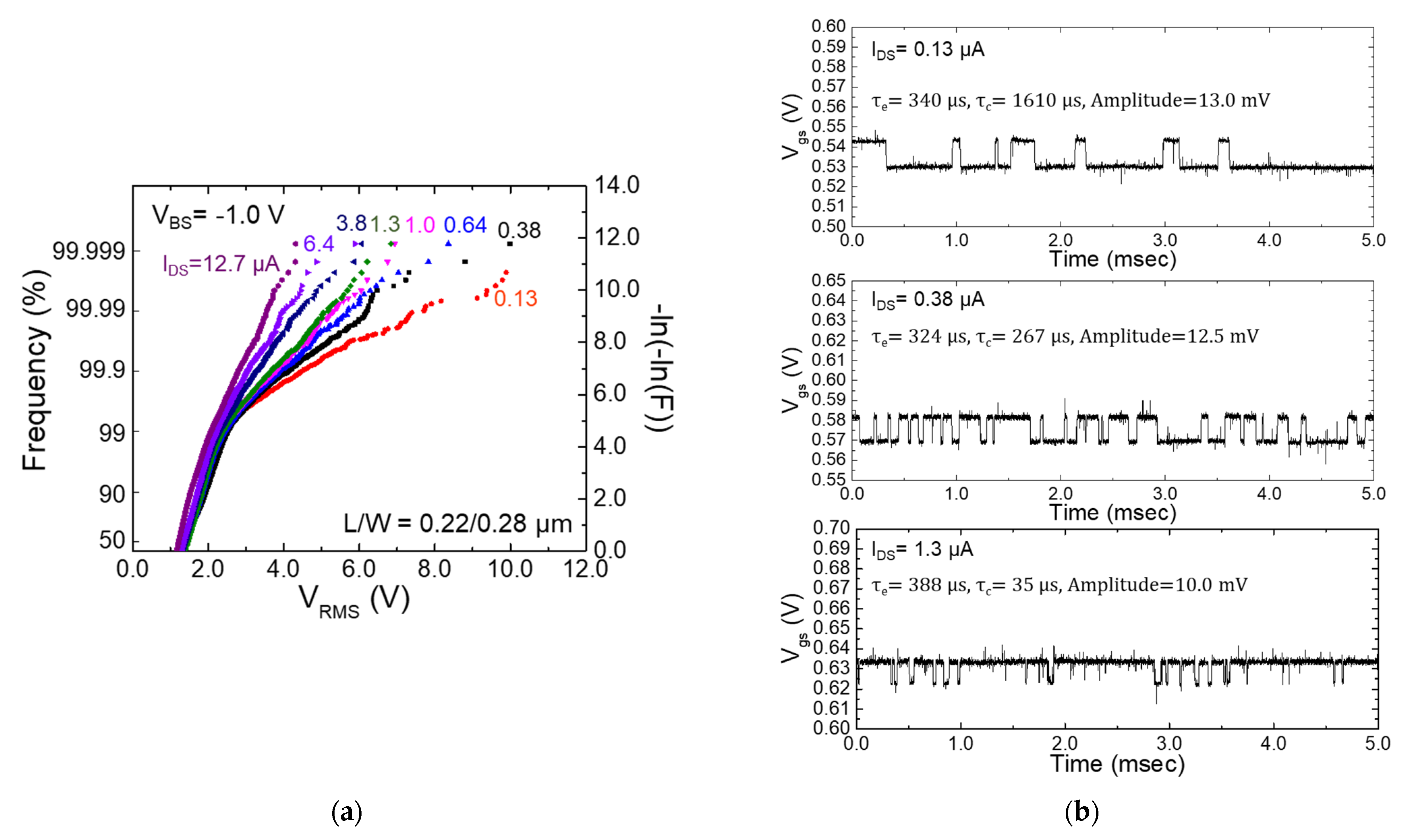
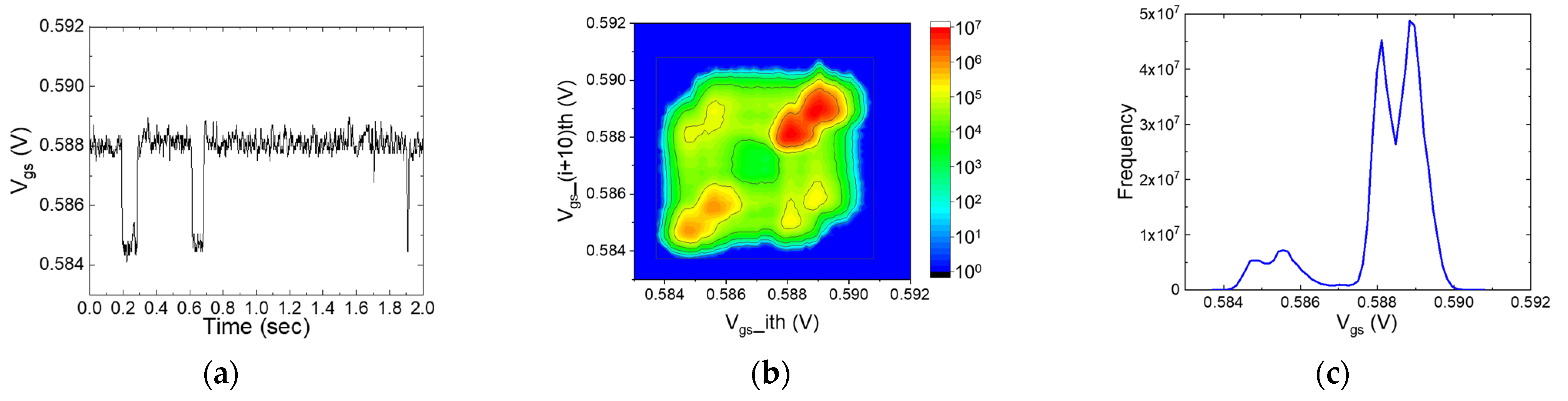
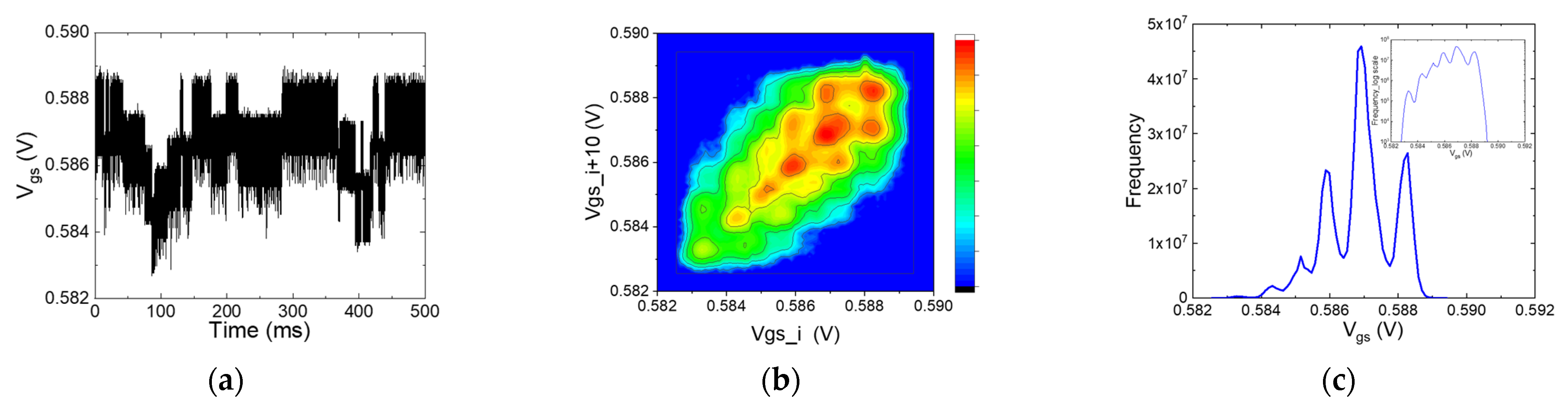
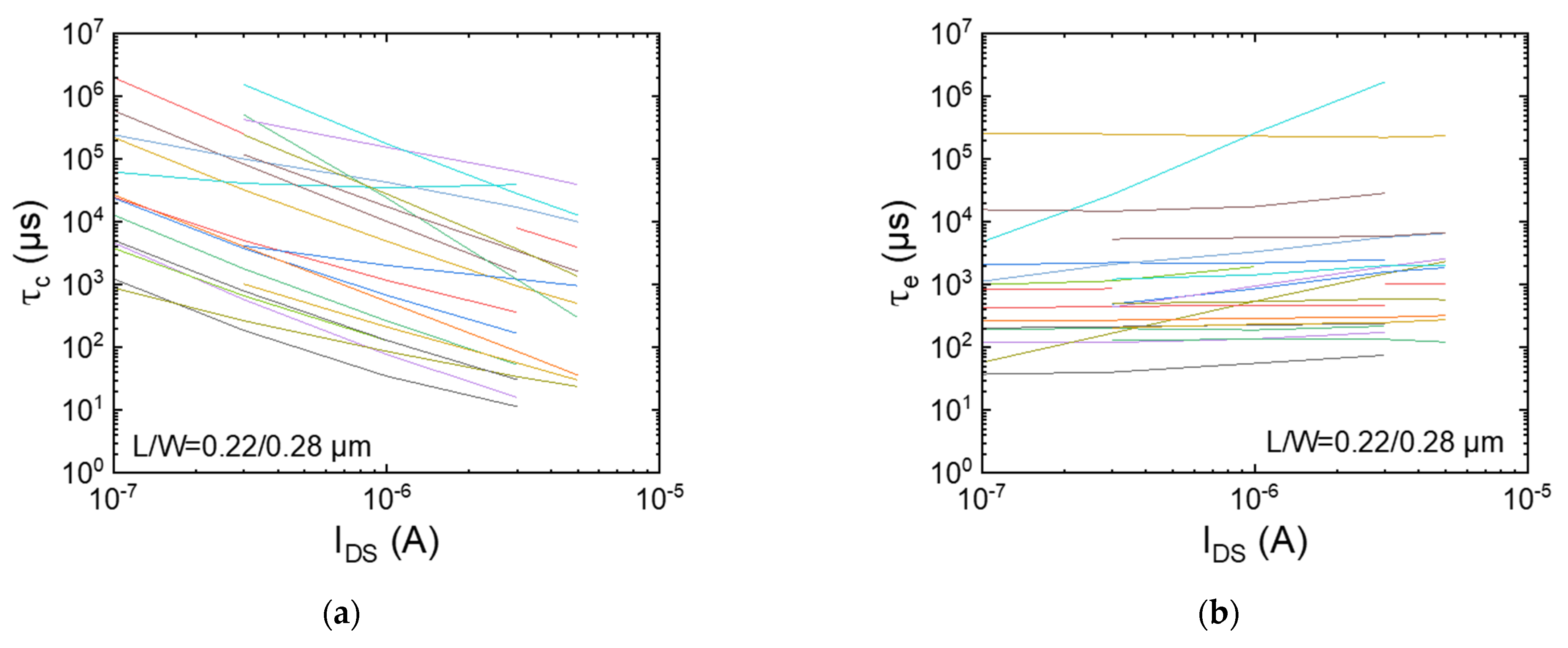
3.3. Time Constants in Individual RTN

As the extraction of multi-trap phenomena is difficult, as discussed in Section 3.2, we discuss the time constants and amplitude only in two-state RTN [59]. Figure 16 shows (a) τc and (b) τe as a function of IDS, respectively. These data are measured at IDS of 0.1, 0.3, 1.0, 3.0, and 5.0 μA. The data in Figure 16 show how parameters from all two-level RTN can be extracted in common under four or five IDS, and thus, the number of selected data points was 22.
Figure 17a shows τce and ET-EF as a function of IDS and Figure 17b band diagram of MOS structure for changing VGS (IDS). τce and ET-EF are calculated from the data in Figure 16 and Equation (12), respectively. τc and τe decrease and increase with an increase in IDS (VGS), and the absolute slope of τc is significantly larger than that of τe. Large trap energy (ET) decreases with an increase in VGS than that of channel electron (EC: bottom energy of conduction band). Then, with increasing VGS (IDS), the energy barrier from the channel electron to the trap decreases and that from the trapped electron to the channel increases. As a result, the time to capture and time to emission decreases and increases, respectively, with increasing VGS (IDS). The transition probability depends on the energy barrier height between a trap and channel. τe depends only on the energy barrier because only one electron is captured in a trap. Meanwhile, τc depends not only on the energy barrier, but also on the number of electrons in a channel because the number of channel electrons increases as VGS (IDS) increases. Then, the dependency of τc on IDS is more significant than that of τe. ET-EF in Figure 17 changed by approximately 175 mV during IDS (VGS) from 0.1 (0.53V) to 5.0 μA (0.75V). Based on these values, ET-EF changes by 0.18 V, whereas VGS changes by 0.22 V. The distance between the traps and the channel was 4.6 nm due to the gate oxide thickness of 5.7 nm. However, τc depends not only on the trap energy, but also on the number of channel electrons; thus, ET-EF values cannot be calculated using Equation (12). The distance is considered to be shorter than the calculated value. τe values for almost all samples monotonically increased with increasing IDS. This suggests that the distance from the trap to the channel is shorter than that to the gate electrode. The distance between the trap and channel is shorter than 2.85 nm, which is the center of the gate oxide thickness. Figure 18a,b show the amplitude and transition frequency as a function of IDS for the same samples as those in Figure 16 and Figure 17, respectively. For a sufficiently long measuring period, the transition frequency (TF) was calculated using the following equation.
TF N e τ e N c τ c
The amplitude decreases and the TF increases with an increase in IDS for almost all samples. This is caused by the increase in the number of channel electrons as IDS increases. However, the amplitude and TF of some samples did not exhibit monotony, which is due to the percolation channel effect [46,47,48,49]. The distance between the channel and trap changes as IDS (VGS) changes because of the formation of the percolation channel.

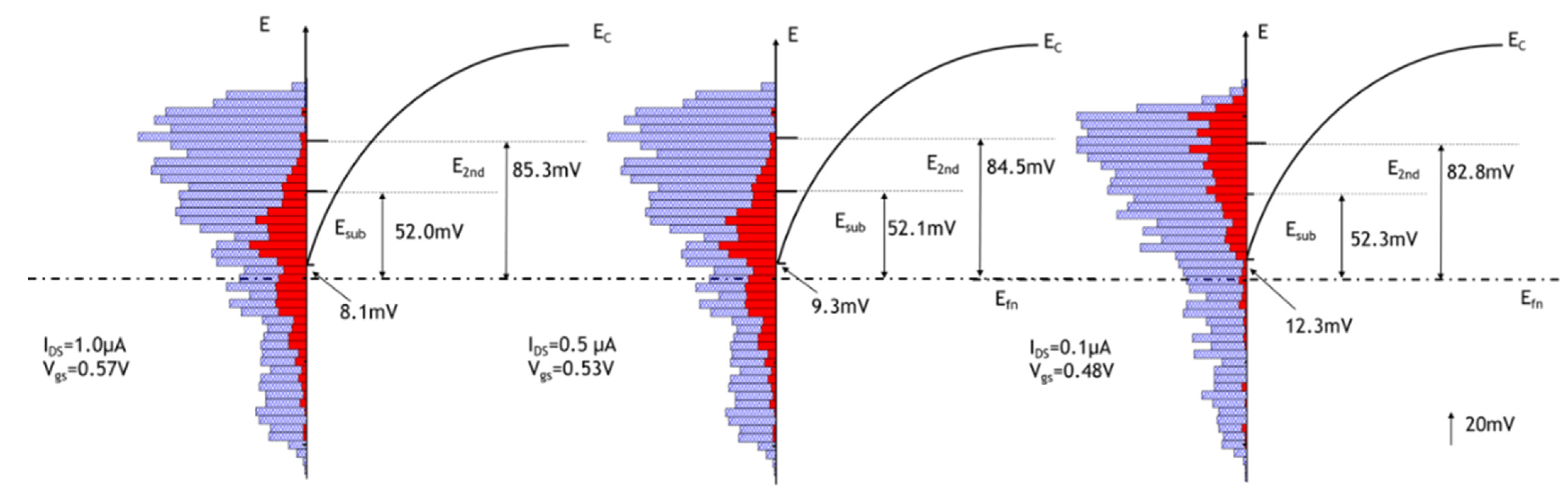
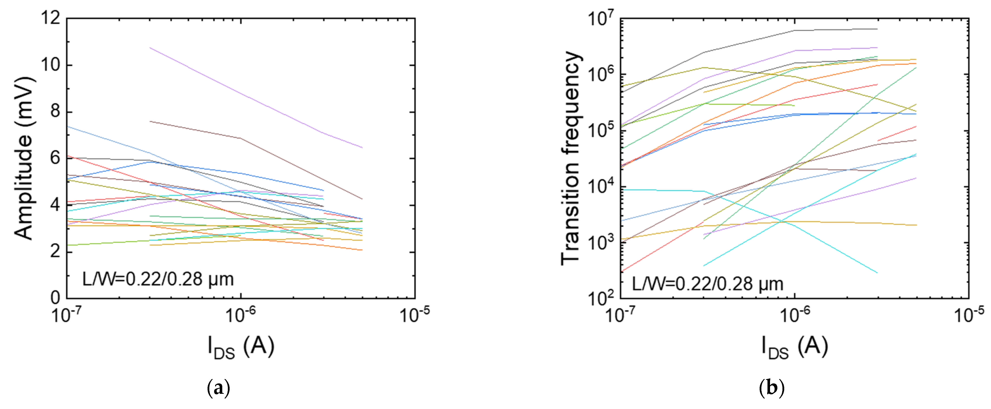
3.4. Effect of Drain Current on Appearance Probability and Amplitude

Figure 19 shows the Gumbel plot of the VRMS for 18,048 MOSFETs. IDS varied from 0.1 to 20 μA. The floor noise in this experiment was smaller than the others and was approximately 35 μVRMS [60]. In Figure 7, VRMS decreases with an increase in IDS for all VRMS. In Figure 19, larger VRMS can also be observed in small IDS in relatively large VRMS regions. However, the higher appearance probability in large IDS than that in small IDS for the small VRMS region of less than 500 μV could not be observed in Figure 7 because the floor noise was approximately 1 mV in that experiment. The amplitude characteristics are the same as the VRMS characteristics, and the distribution of the time constants is the same for all conditions [60]. Figure 20 shows the frequency of RTN with two, three, and more than three states in 18,048 MOSFETs. The frequency of all states increases with IDS.
It is assumed that the probability that electrons and percolation paths are close to each other increases as IDS increases, increasing the number of electrons in the channel and the number of percolation paths. Figure 21 shows the Gumbel plot for the amplitude of two-state RTN. Notably, frequency sometimes increases with an increase in IDS even though the effect of trapped electrons on the channel decreases with an increase in the electron density in the channel.

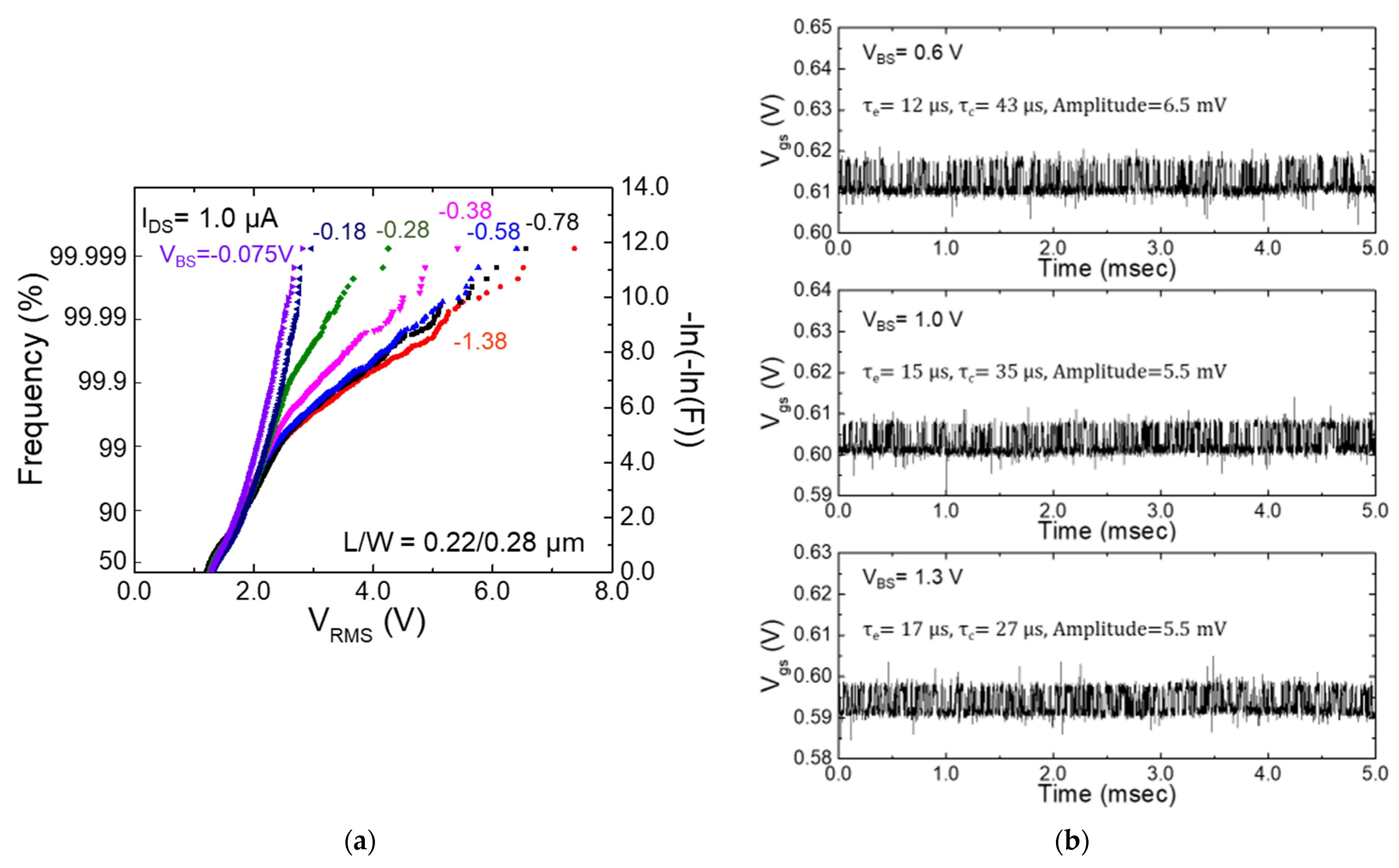
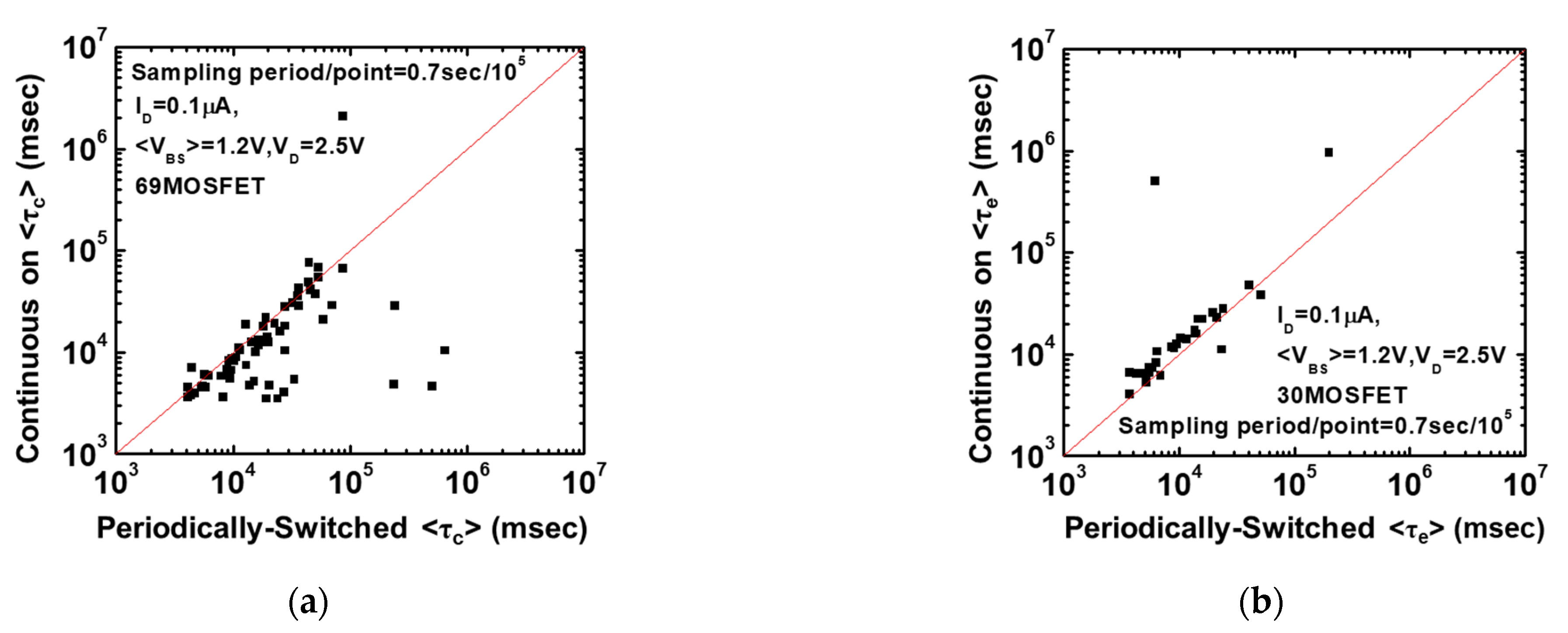
3.5. Modulation of Time Constants

In Section 3.3, the time constants were measured under constant conditions. The differences between time constants and VRMS in continuous on-state and periodically switched conditions are discussed in this section [61]. As shown in Figure 16, VGS dependance on τc is larger than that of τe, and this suggests that the cycle period (τc + τe) in on-state is longer than that in off-state because the VGS of off-state is smaller than that of on-state. Figure 21a,b show the time constant relationship between continuous on-state and periodically switched conditions. In the periodically switched condition, MOSFETs cycled for 10.6 msec in 700 ms, which was a measurement cycle. Although τe of almost all samples are the same in both conditions, τc of some samples in the periodically switched condition is larger than that in continuous on-state. Figure 22 shows (a) histogram of the VRMS difference between continuous on-state and periodically off-state (ΔVRMS) and (b) schematic waveform of RTN in continuous on-state and periodically off-state, respectively. Though VRMS of 5% samples was increased, that of 95% was not changed or decreased in the periodically switched condition. As a result, VRMS decreased in the periodically switched condition, with a few exceptions. This suggests that VRMS can be reduced by the modulation of operation conditions, even in the same MOSFET.

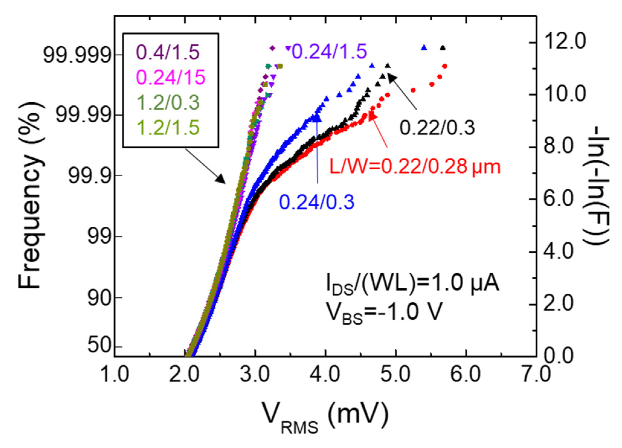
3.6. Device Structure Dependence of RTN

In the above results and discussions in Section 3.1, Section 3.2, Section 3.3, Section 3.4 and Section 3.5, the dependance of RTN characteristics on operation conditions is mainly described. In Section 3.6, the dependance of RTN characteristics on the structure of MOSFETs, such as buried channel MOSFETs and asymmetric source–drain structure MOSFETs, are described [57,62,63,64,65].

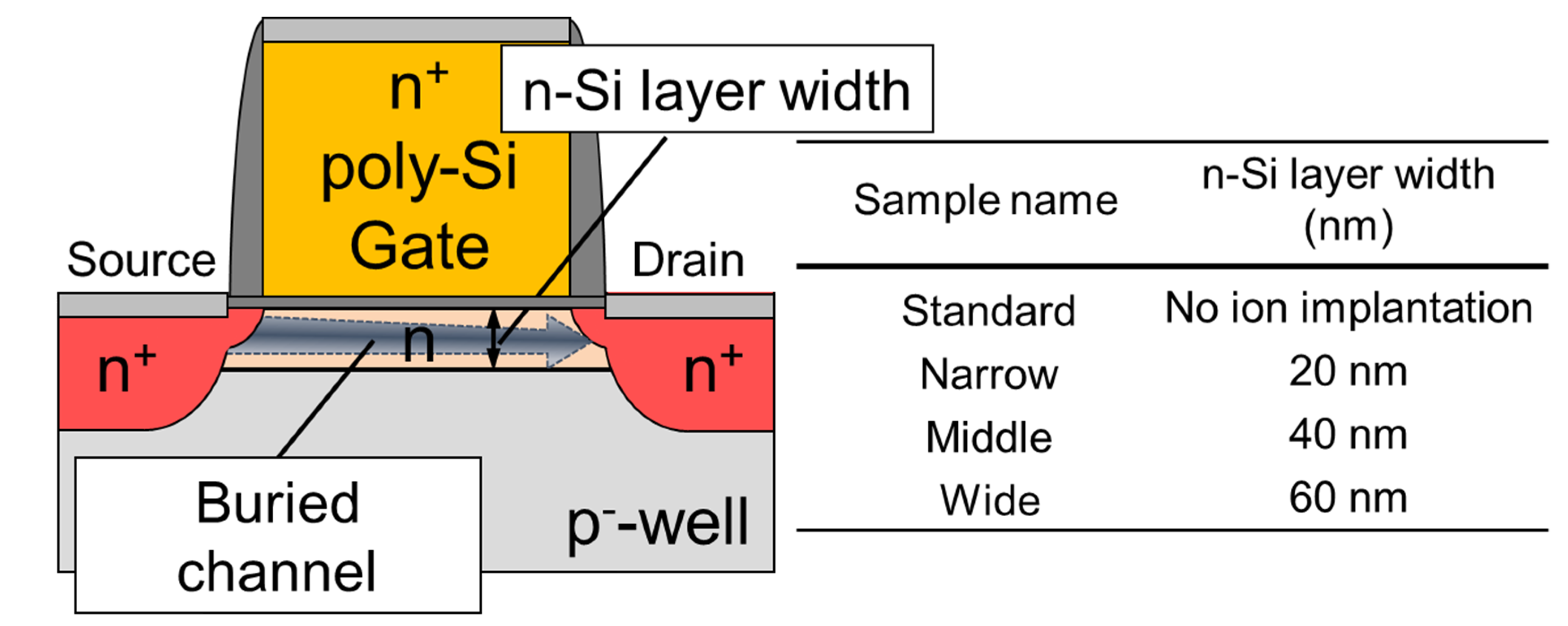
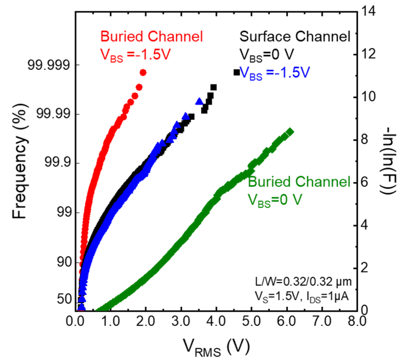
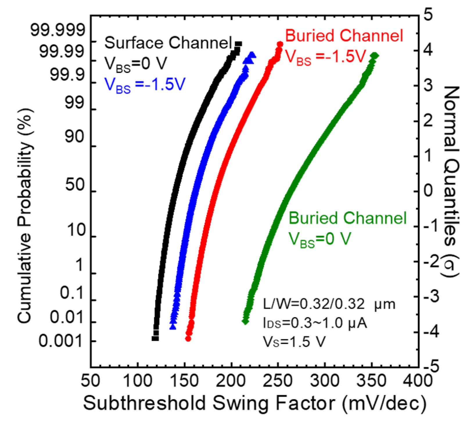
3.6.1. Buried Channel MOSFETs

Figure 23 shows the structure of buried channel MOSFETs studied in this work. To discuss the effects of n-Si layer widths and the distance between the channel and SiO2/Si interface, n-Si layer width was varied to be 0, 10, 25, and 60 nm for standard, narrow, middle, and deep samples formed by arsenic ion implantation, respectively, and the high-energy ion implantation created not only a deep channel, but also a wide channel in the vertical direction to the SiO2/Si interface. Figure 24 and Figure 25 show the Gumbel plots of VRMS for the standard, narrow, middle, and deep samples and the VBS dependance of VRMS for the narrow, middle, and deep samples, respectively [57,65].
The channel length and width were 0.22 and 0.28 μm, respectively, IDS was 100 nA, and VBS in Figure 24 was −1.5 V and varied from −1.0 V to −2.0 V in Figure 25, respectively. The VRMS values for the standard and Narrow samples are the same, and the frequency of large VRMS decreases with an increase in n-Si width and/or depth. This means that RTN cannot be decreased by the 20 nm buried channel, but can be decreased by forming a buried channel of 40 nm and more. By increasing the back bias, VRMS increases for all samples, and the effect of VBS remarkably appeared for the wide sample. By applying the back bias, the channel pushes onto the SiO2/Si interface, and the channel thickness decreases. The buried channel is extremely effective for decreasing RTN because the channel is separated from SiO2/Si interface and the wide channel becomes difficult to form the percolation path. Furthermore, the buried channel MOSFET in the isolated well was employed to evaluate VBS dependance [64], and VBS can be varied from 0 V in this structure because the well voltage can be changed freely. The gate length and gate width of the MOSFETs are 0.32 and 0.32 μm, respectively, IDS was 1 μA, vs. was 1.5 V, and Vwell of the normal well and isolated well were 0 and 1.5 V, respectively; thus, VBS was set at −1.5 and 0 V for the normal well and isolated well, respectively.
Figure 26 shows the Gumbel plot of the VRMS for the buried channel and surface channel MOSFETs with the back bias conditions of 0 and −1.5 V. VRMS of the buried channel MOSFETs at VBS = −1.5 V is significantly less than those of surface channel; however, that at VBS = 0 V is larger than those of the surface channel even though those of the surface channel do not depend on VBS. Figure 27 shows the normal probability plot of the subthreshold swing for the same sample of Figure 26. The subthreshold swing of buried channel MOSFETs with VBS = 0 is much smaller than the others. A strong relationship between the subthreshold swing and VRMS has been reported [64]. The result strongly suggests that the increase in VRMS is enlarged by the physical origin, which increases the subthreshold swing, and the origin is an enhancement of the percolation path formation [64]. Note that RTN has to be enhanced by a minimal small gate control effect on the channel. Furthermore, the variability of the threshold voltage is increased using the buried channel MOSFETs; thus, we cannot introduce buried channel MOSFETs when the fixed pattern noise is critical for device performance.

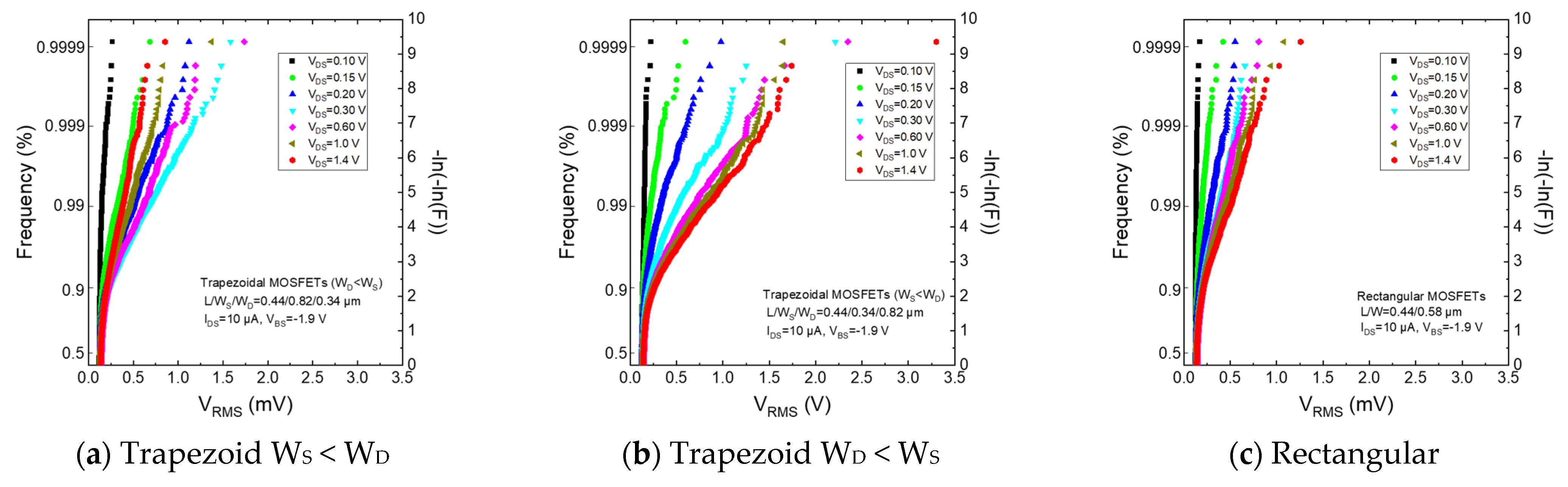
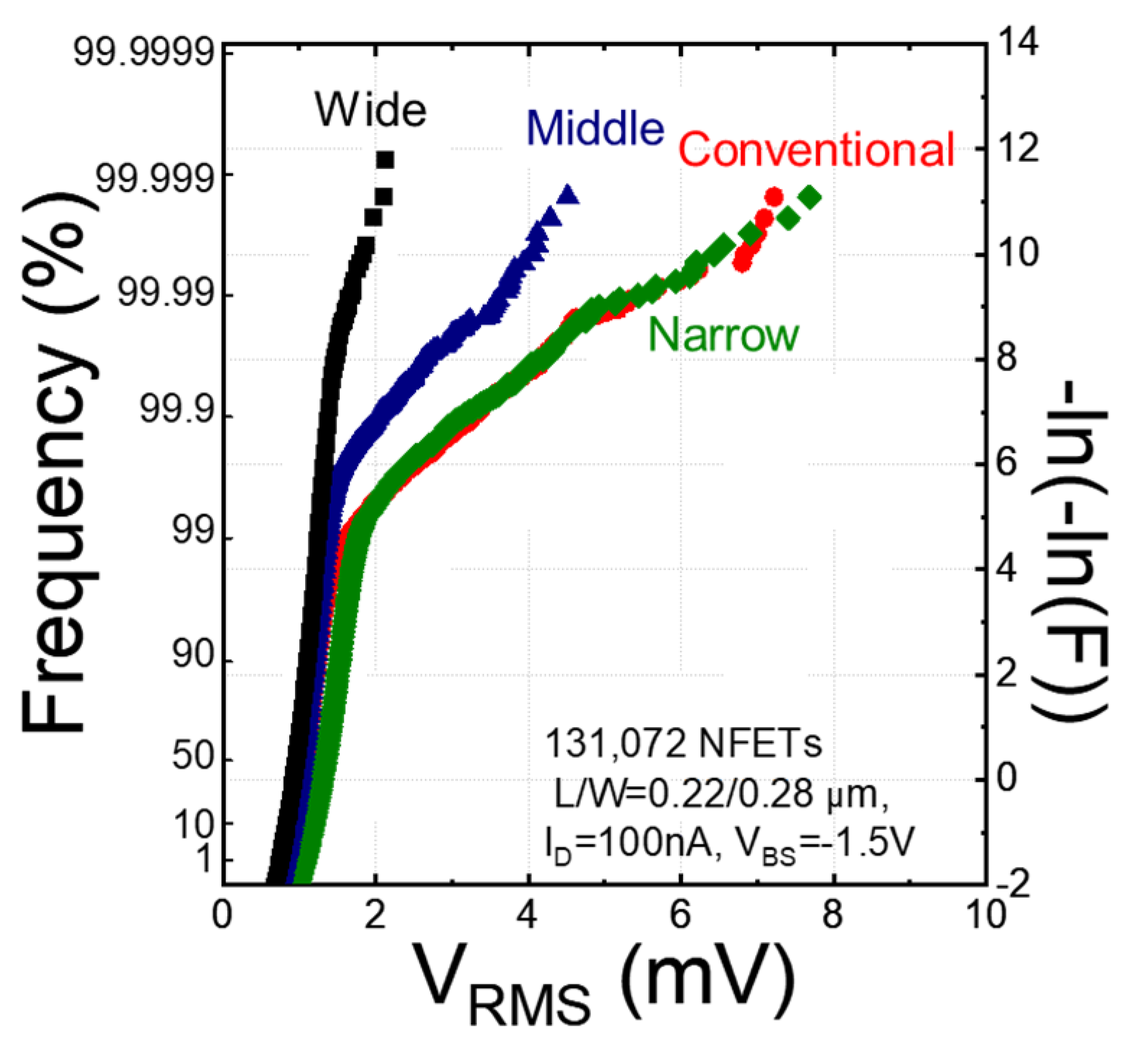
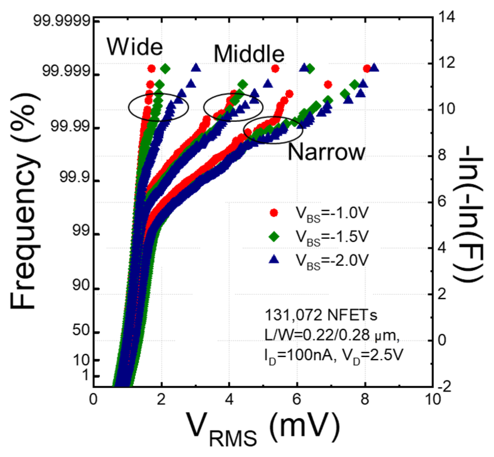
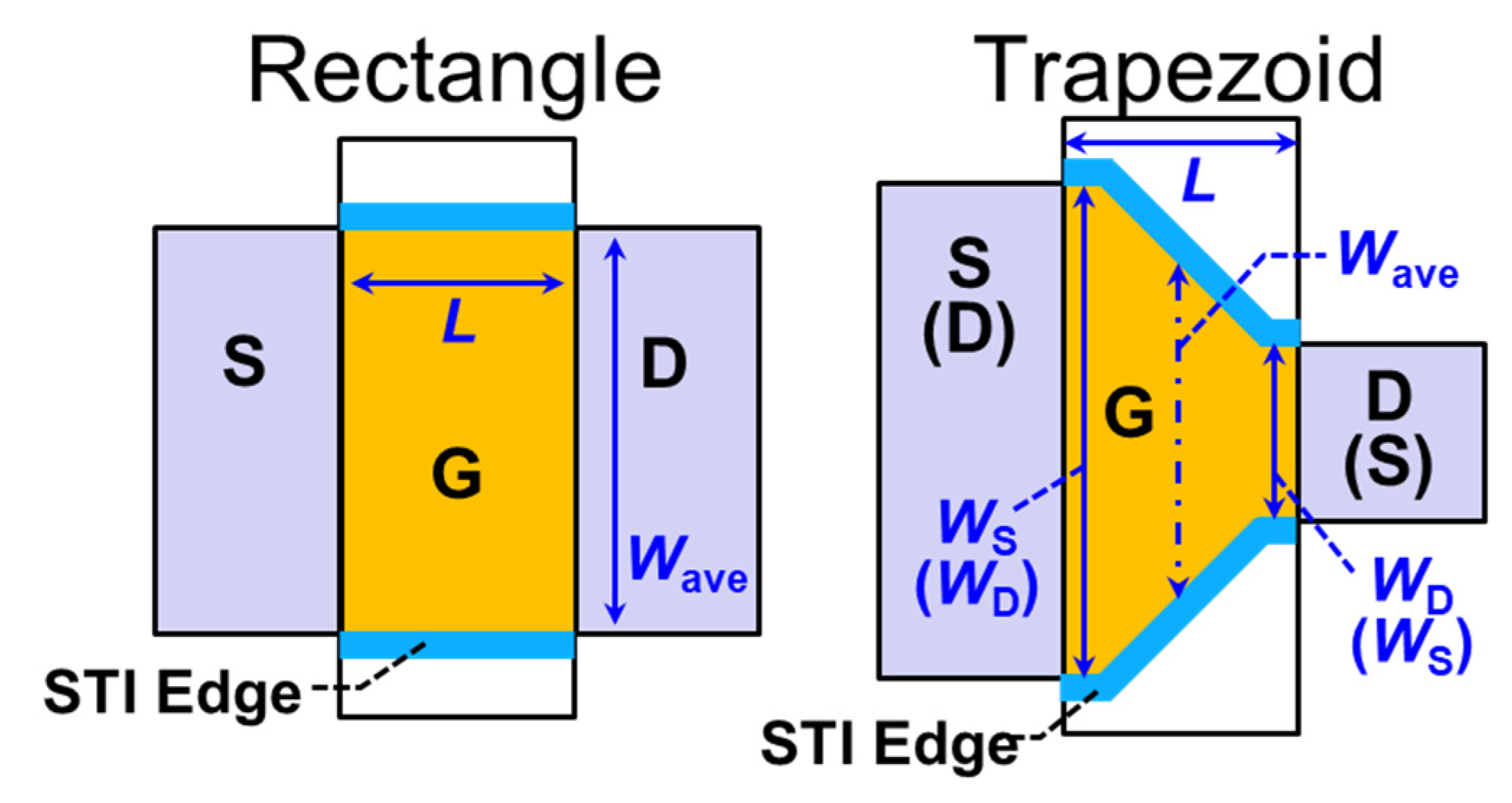
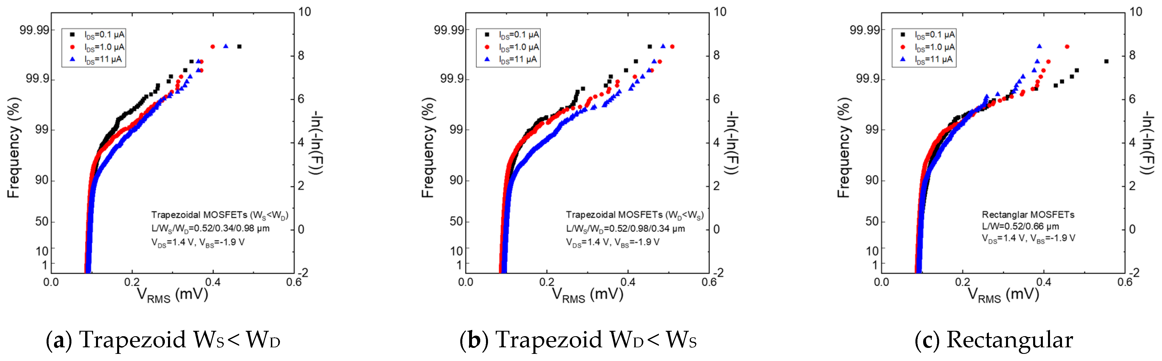
3.6.2. Asymmetry Source and Drain Width MOSFETs

Figure 28 shows the layout structure of rectangular and trapezoidal shape MOSFETs used in this experiment [62,63]. In the trapezoidal MOSFETs, when current flows from the left to right direction, the source has a wide gate width, and when current flows from the right to left direction, the source has a shallow gate width. The Gumbel plots of VRMS for trapezoidal ((a)WD < WS and (b) WS < WD) and (c) rectangular MOSFETs are shown in Figure 29 [62]. The gate width of rectangular MOSFETs was set as the average of the gate width of trapezoidal MOSFETs. IDS was varied from 0.1 to 11 μA for constant VBS of −1.9 V and VDS of 1.4 V. In (c) rectangular MOSFETs, similar phenomena, as shown in Figure 19, are obtained. In contrast, in the trapezoidal MOSFETs, VRMS increases with an increase in IDS (VGS), and those of WD < WS are larger than those of WS < WD. VDS is larger than VGS in this experiment. MOSFETs were operated in the saturation region, and the channel formed near the source. Increasing IDS increases electron density in the channel, and the electron density at the source of MOSFETs with WD < WS is less than that with WS < WD. These characteristics indicate that the influence of a charged trap reduces at a high carrier density condition [39,60,62]. This means that the electron density and the location in the channel are important factors affecting RTN characteristics. RTN characteristics were evaluated for various VDS using rectangular and trapezoidal MOSFETs.
Figure 30 shows the Gumbel plots of VRMS for trapezoidal ((a) WD < WS and (b) WS < WD) and (c) rectangular MOSFETs. VDS was varied from 0.1 V to 1.4 V for constant IDS of 10 μA and VBS of −1.9 V [63]. The VDS dependance of VRMS for the (c) rectangular and (b) trapezoidal with WS < WD MOSFETs is the same, and VRMS increases as VDS increases, monotonically. The dependance of (b) trapezoidal with WS < WD on VDS is larger than that of rectangular MOSFETs. In contrast, VRMS increases with an increase in VDS at less than 0.3 V; however, VRMS decreases with an increase in VDS at >0.3V for trapezoidal MOSFETs with WS > WD. When VDS is smaller than the pinch-off voltage (VGS-VTH = 0.3 V in this experiment), the channel is uniformly formed under the gate oxide, and the channel vanishes at the drain edge at the pinch-off voltage. The vanished region expands with increasing VDS. On the other hand, IDS was set at a constant of 10 μA, and this means that VGS decreases as VDS increases at less than a pinch-off voltage of 0.3V. In rectangular MOSFETs, VRMS increases with a decrease in VGS, which is the same effect as shown in Figure 7. In trapezoidal MOSFETs with WS < WD, VDS dependance was enhanced by reducing the channel width. In trapezoidal MOSFETs with WD < WS, VDS dependance is the same as others at less VDS than a pinch-off voltage of 0.3 V. However, the opposite dependency is obtained at larger VDS than the pinch-off voltage. It is considered that the apparent gate width of MOSFETs (WD < WS) increases when the pinch-off point reaches the source, and then, the size effect of VRMS shown in Figure 6 is obtained. These data imply that the noise strength depends heavily on operation conditions, which means that the location and electron density in a channel are critical for RTN generation.
Although using trapezoidal MOSFETs in real electronic devices is difficult, changing the shape of MOSFETs is very useful to obtain much information about RTN characteristics. For example, the effect of trap at the isolation edge can be evaluated using octagonal MOSFETs, which have only a gate edge and no shallow trench isolation edge [62].

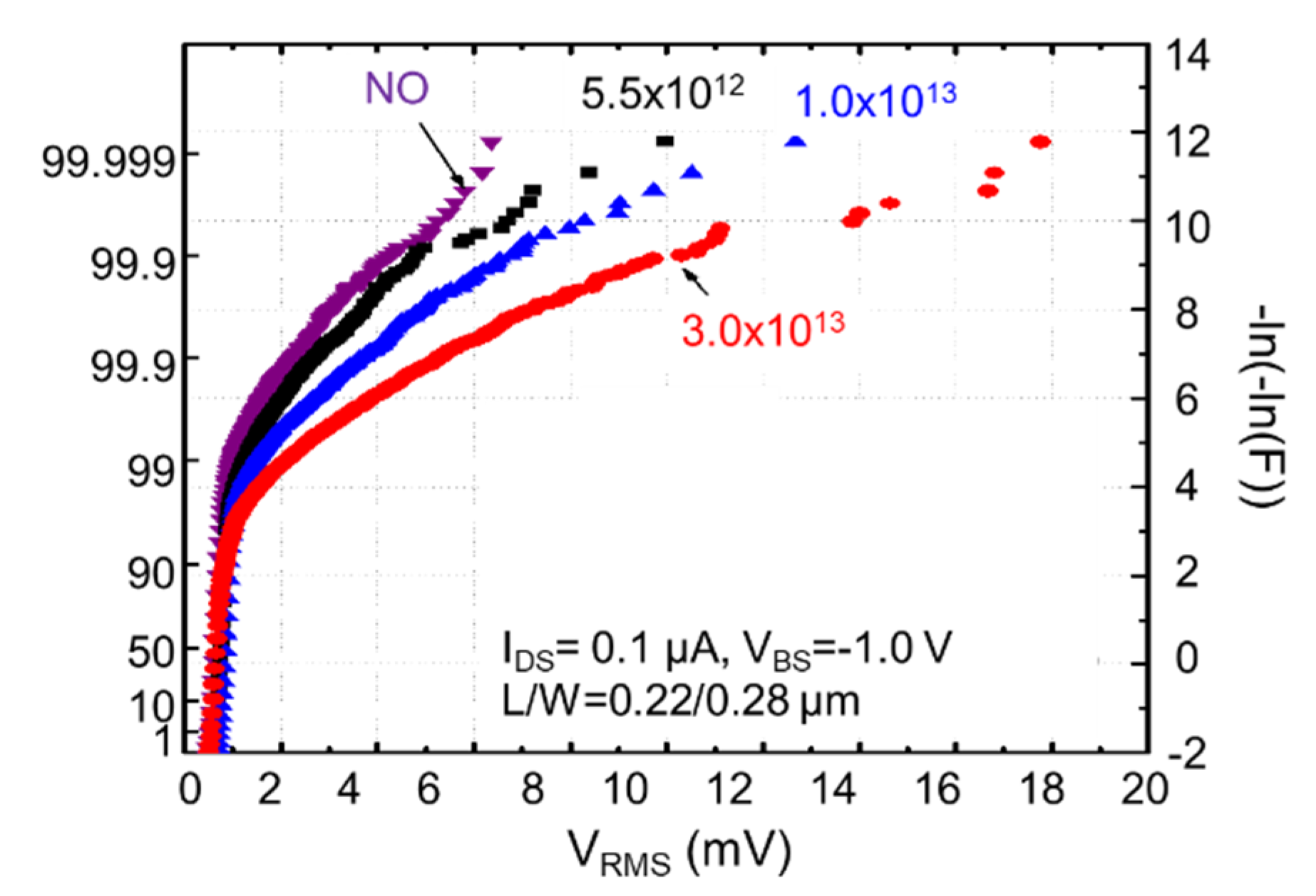
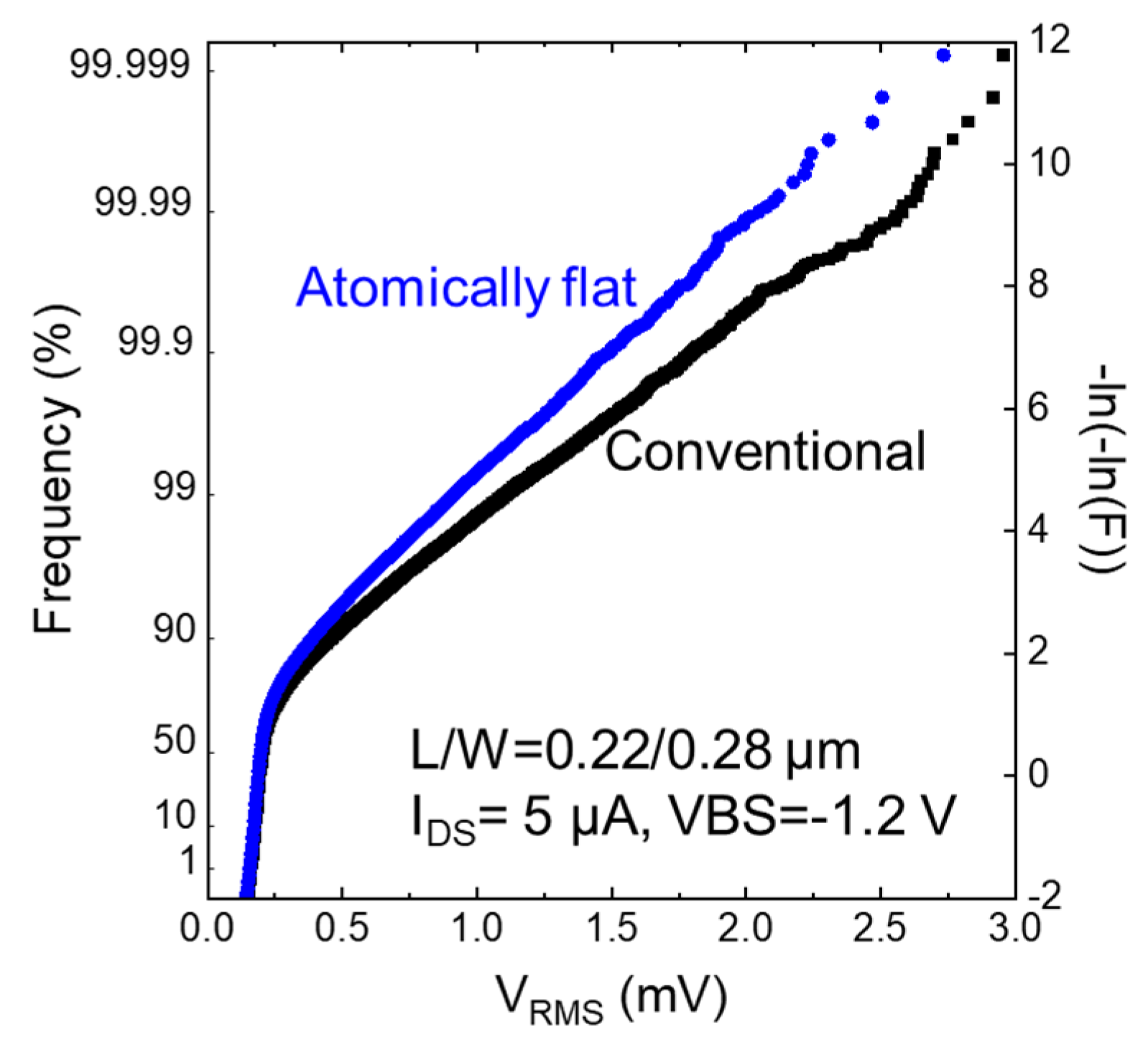
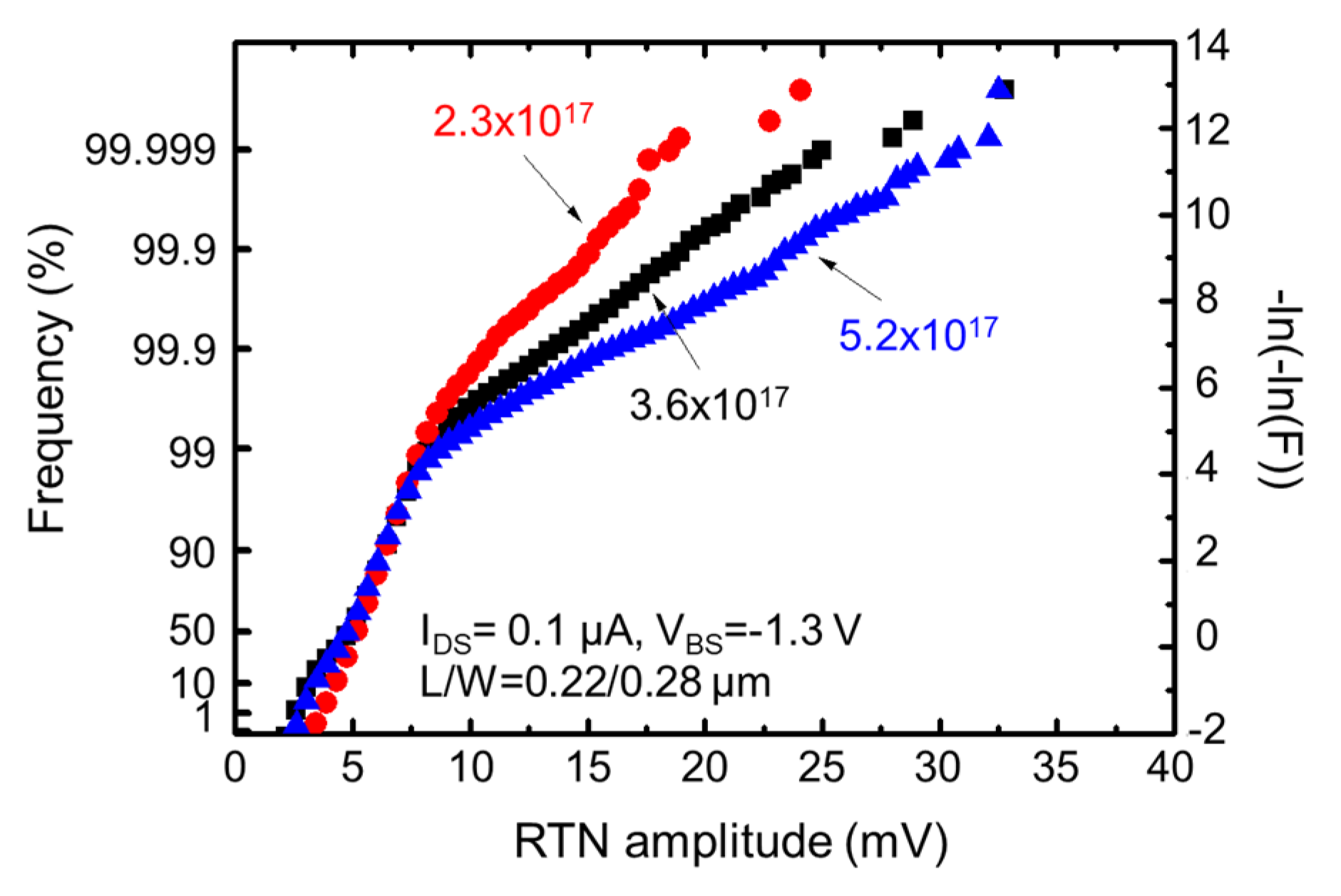
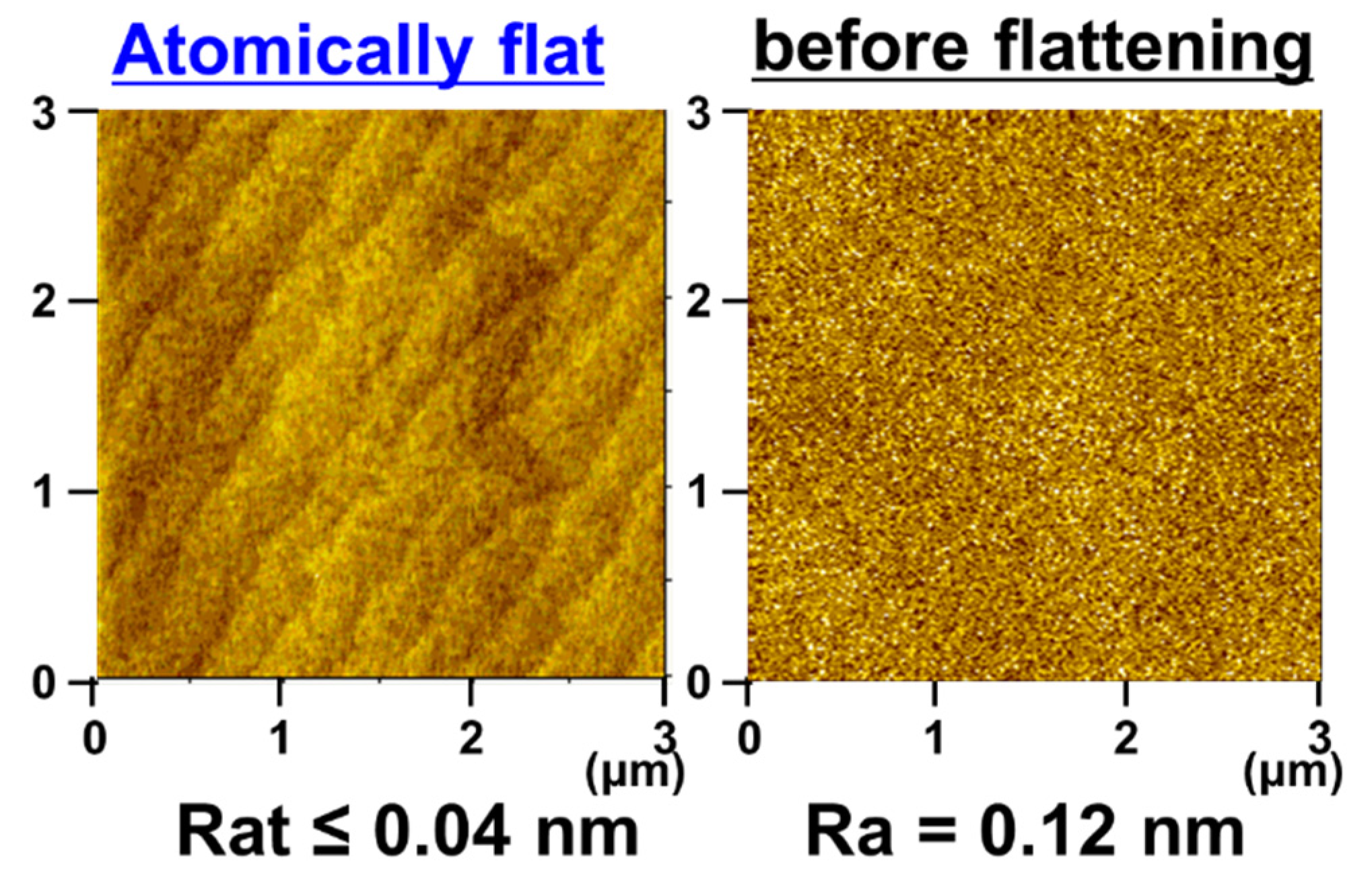
3.6.3. MOSFETs with Atomically Flat Gate Insulator/Si Interface

The roughness of the interface between the gate insulator and Si is essential for MOSFETs. The interface roughness degrades not only electron mobility [66,67,68,69,70,71] and gate dielectric reliability [72,73,74], but also noise generation [71,75,76]. An atomically flat interface [77,78,79,80,81,82,83,84] is effective for reducing low-frequency noise [79,83,84,85,86,87].
Figure 31 shows images of an atomically flat surface and as-received Si(100) measured by atomic force microscopy (AFM). The atomically flat surface was formed in the active region with shallow trench isolation and was measured after the gate oxide formation and following oxide stripping [84]. The average roughness (Ra) of the conventional surface is 0.12 nm, which is the same as the initial surface of Si(100). In an atomically flat surface, a step and terrace structure can be obtained, and the step height is the same as the monoatomic step length of Si(100) of 0.135 nm. The terrace width (L) is defined by the following equation using the off-angle (θ) to the just (100) orientation. The average roughness in the trace of the atomically flat interface was less than 0.04 nm, which is the detection limit of our AFM system.
L = 0.135 tan θ   ( nm )
Figure 32 shows the Gumbel plot of VRMS for the atomically flat and conventional SiO2/Si interface [84]. The noise of the atomically flat interface is less than that of the conventional interface. This means that introducing the atomically flat interface is extremely effective for reducing RTN as well as 1/f noise [86,87,88]. The atomically flat surface was formed before gate oxidation in this experiment [84].
To implement the surface flattening process, a low temperature of less than 900 °C and low oxidation species, such as O2 and H2O, must be required [81,82,85]. There is another method for flattening the surface first and keeping it during the process steps preceding gate oxidation [85,87,88]. Other problems exist, such as STI edge shape and dopant segregation, and the solutions to these problems may affect not only MOSFET characteristics, but also noise [84]. The flattening process just before the gate oxidation is superior to the flattening process in the first step for introducing interface flattening between SiO2 and Si, and this can be obtained by low temperature Ar annealing by reducing oxidation species.

4. Conclusions

The importance of low-frequency noise in LSI, and various effects on RTN, such as MOSFETs’ size, bias and operation conditions, and device structures, are described. The measurement technique using the array test circuit and the extraction of important parameters (time constants and amplitude) in RTN characteristics are also described. Time constants can be extracted essentially using classical equations; however, it is not as simple when downsizing MOSFETs and reducing the number of channel electrons, and the percolation path is formed. Variability of low-frequency noise increases with shrinkage of MOSFETs. In this paper, we evaluated relatively large planer MOSFETs (L = 0.22~0.4 μm), unfortunately. The size of MOSFETs has been downscaled to less than l0 nm and the structure has changed the planer to FinFET, recently. We have to continue the evaluation of such miniaturized and new structure devices. To assess the effect of this noise on MOSFETs, we have to understand their characteristics statistically, and then, sufficient samples must be accurately evaluated in a short period.

Funding

This research received no external funding.

Acknowledgments

The author acknowledges Shigetoshi Sugawa, Rihito Kuroda, Tetsuya Goto, Tomoyuki Suwa, Keninchi Abe, Philippe Gaubert, Yuki Kumagai, Takafumi Fujisawa, Hiroyuki Suzuki, Akihiro Yonezawa, Toshiki Obara, Takezo Mawaki, Shinya Ichino, Ryo Akimoto, and Tatsuki Ueta for their measurements and useful discussions and Yutaka Kamata and Katsuhiko Shibusawa for fabrication of the array test circuit and useful discussions.

Conflicts of Interest

The authors declare no conflict of interest.

References

  1. Dennard, R.H.; Gaensslen, F.H.; Kuhn, L.; Yu, H.N. Design of micron MOS switching devices. In Proceedings of the 1972 International Electron Devices Meeting, Washington, DC, USA, 4–6 December 1972; pp. 168–170. [Google Scholar]
  2. Dennard, R.H.; Gaensslen, F.H.; Rideout, V.L.; Bassous, E.; LeBlanc, A.R. Design of ion-implanted MOSFET’s with very small physical dimensions. IEEE J. Solid-State Circuits 1974, 9, 256–268. [Google Scholar] [CrossRef] [Green Version]
  3. Moore, G.E. Cramming more components onto integrated circuits. Electronics 1965, 38, 114. [Google Scholar] [CrossRef]
  4. Boukhbza, J.; Plivier, P. Flash Memory Integration -Performance and Energy Considerations; Elsevier Ltd.: Oxford, UK, 2017. [Google Scholar]
  5. Parameswaran, S.; Hui, G. Power consumption in CMOS combinational logic blocks at high frequencies. In Proceedings of the ASP-DAC ‘97: Asia and South Pacific Design Automation Conference, Chiba, Japan, 28–31 January 1997; pp. 195–200. [Google Scholar]
  6. Appuswamy, R.; Olma, M.; Ailamaki, A. Scaling the Memory Power Wall With DRAM-Aware Data Management. In Proceedings of the 11th International Workshop on Data Management on New Hardware, Melbourne, VIC, Australia, 31 May–4 July 2015. [Google Scholar]
  7. Poess, M.; Nambiar, R.O. Energy cost, the key challenge of today’s data centers: A power consumption analysis of TPC-C results. In Proceedings of the 34th International Conference on Very Large Data Bases, Auckland, New Zealand, 23–28 August 2008; pp. 1229–1240. [Google Scholar]
  8. Karyakin, A.; Salem, K. An analysis of memory power consumption in database systems. In Proceedings of the 13th International Workshop on Data Management on New Hardware, Chicago, IL, USA, 15 May 2017. [Google Scholar]
  9. Carter, J.; Rajamani, K. Designing Energy-Efficient Servers and Data Centers. Computer 2010, 43, 76–78. [Google Scholar] [CrossRef]
  10. Ohmi, T.; Hirayama, M.; Teramoto, A. New era of silicon technologies due to radical reaction based semiconductor manufacturing. J. Phys. D Appl. Phys. 2006, 39, R1–R17. [Google Scholar] [CrossRef]
  11. Uren, M.J.; Day, D.J.; Kirton, M.J. 1/f and random telegraph noise in silicon metal-oxide-semiconductor field-effect transistors. Appl. Phys Lett. 1985, 47, 1195–1197. [Google Scholar] [CrossRef]
  12. Kirton, M.J.; Uren, M.J. Noise in solid-state microstructures: A new perspective on individual defects, interface states and low-frequency (1/f) noise. Adv. Phys. 1989, 38, 367–468. [Google Scholar] [CrossRef]
  13. Christensson, S.; Lundström, I.; Svensson, C. Low frequency noise in MOS transistors—I Theory. Solid State Electron. 1968, 11, 797–812. [Google Scholar] [CrossRef]
  14. Toita, M.; Vandamme, L.K.J.; Sugawa, S.; Teramoto, A.; Ohmi, T. Geometry and bias dependence of low-frequency random telegraph signal and 1/f noise levels in mosfets. Fluct. Noise Lett. 2005, 5, L539–L548. [Google Scholar] [CrossRef]
  15. Sugawa, S. The Advanced Technology of the Semiconductor Integrated Circuits Needs the “Analog Intelligence” Again. DENSO Tech. Rev. 2005, 10, 3–9. (In Japanese) [Google Scholar]
  16. Leyris, C.; Martinez, F.; Valenza, M.; Hoffmann, A.; Vildeuil, J.C.; Roy, F. Impact of Random Telegraph Signal in CMOS Image Sensors for Low-Light Levels. In Proceedings of the 32nd European Solid-State Circuits Conference, Montreux, Swizerland, 19–21 September 2006; pp. 376–379. [Google Scholar]
  17. Wang, X.; Rao, P.R.; Mierop, A.; Theuwissen, A.J.P. Random Telegraph Signal in CMOS Image Sensor Pixels. In Proceedings of the International Electron Devices Meeting, San Francisco, CA, USA, 11–13 December 2006; pp. 115–118. [Google Scholar]
  18. Chao, C.Y.-P.; Tu, H.; Wu, T.M.-H.; Chou, K.-Y.; Yeh, S.-F.; Yin, C.; Lee, C.-L. Statistical Analysis of the Random Telegraph Noise in a 1.1 μm Pixel, 8.3 MP CMOS Image Sensor Using On-Chip Time Constant Extraction Method. Sensors 2017, 17, 2704. [Google Scholar] [CrossRef] [PubMed] [Green Version]
  19. Chao, C.Y.-P.; Yeh, S.-F.; Wu, M.-H.; Chou, K.-Y.; Tu, H.; Lee, C.-L.; Yin, C.; Paillet, P.; Goiffon, V. Random Telegraph Noises from the Source Follower, the Photodiode Dark Current, and the Gate-Induced Sense Node Leakage in CMOS Image Sensors. Sensors 2019, 19, 5447. [Google Scholar] [CrossRef] [Green Version]
  20. Kuroda, R.; Teramoto, A.; Sugawa, S. Impacts of Random Telegraph Noise with Various Time Constants and Number of States in Temporal Noise of CMOS Image Sensors. ITE Trans. Media Technol. Appl. 2018, 6, 171–179. [Google Scholar] [CrossRef]
  21. Wang, X.; Snoeij, M.F.; Rao, P.R.; Mierop, A.; Theuwissen, A.J.P. A CMOS Image Sensor with a Buried-Channel Source Follower. In Proceedings of the IEEE International Solid-State Circuits Conference, San Francisco, CA, USA, 3–7 February 2008; pp. 62–595. [Google Scholar]
  22. Toh, S.O.; Tsukamoto, Y.; Zheng, G.; Jones, L.; Tsu-Jae King, L.; Nikolic, B. Impact of random telegraph signals on Vmin in 45nm SRAM. In Proceedings of the IEEE International Electron Devices Meeting, Baltimore, MD, USA, 24 July 2020; pp. 767–770. [Google Scholar]
  23. Takeuchi, K.; Nagumo, T.; Takeda, K.; Asayama, S.; Yokogawa, S.; Imai, K.; Hayashi, Y. Direct observation of RTN-induced SRAM failure by accelerated testing and its application to product reliability assessment. In Proceedings of the Symposium on VLSI Technology, 15–17 June 2010; pp. 189–190. [Google Scholar]
  24. Tanizawa, M.; Ohbayashi, S.; Okagaki, T.; Sonoda, K.; Eikyu, K.; Hirano, Y.; Ishikawa, K.; Tsuchiya, O.; Inoue, Y. Application of a Statistical Compact Model for Random Telegraph Noise to Scaled-SRAM Vmin Analysis. In Proceedings of the Symposium on VLSI Technology, Honolulu, HI, USA, 15–17 June 2010; pp. 95–96. [Google Scholar]
  25. Aadithya, K.V.; Demir, A.; Venugopalan, S.; Roychowdhury, J. Accurate Prediction of Random Telegraph Noise Effects in SRAMs and DRAMs. IEEE Trans. Computer-Aided Des. Integr. Circuits Syst. 2013, 32, 73–86. [Google Scholar] [CrossRef] [Green Version]
  26. Compagnoni, C.M.; Gusmeroli, R.; Spinelli, A.S.; Lacaita, A.L.; Bonanomi, M.; Visconti, A. Statistical Investigation of Random Telegraph Noise ID Instabilities in Flash Cells at Different Initial Trap-filling Conditions. In Proceedings of the International Reliability physics symposium, Phoenix, AZ, USA, 15–19 April 2007; pp. 161–166. [Google Scholar]
  27. Tega, N.; Miki, H.; Osabe, T.; Kotabe, A.; Otsuga, K.; Kurata, H.; Kamohara, S.; Tokami, K.; Ikeda, Y.; Yamada, R. Anomalously Large Threshold Voltage Fluctuation by Complex Random Telegraph Signal in Floating Gate Flash Memory. In Proceedings of the International Electron Devices Meeting, San Francisco, CA, USA, 11–13 December 1995; pp. 491–494. [Google Scholar]
  28. Kurata, H.; Otsuga, K.; Kotabe, A.; Kajiyama, S.; Osabe, T.; Sasago, Y.; Narumi, S.; Tokami, K.; Kamohara, S.; Tsuchiya, O. The Impact of Random Telegraph Signals on the Scaling of Multilevel Flash Memories. In Proceedings of the Symposium on VLSI Circuits, Honolulu, HI, USA, 15–17 June 2006; pp. 112–113. [Google Scholar]
  29. Kurata, H.; Otsuga, K.; Kotabe, A.; Kajiyama, S.; Osabe, T.; Sasago, Y.; Narumi, S.; Tokami, K.; Kamohara, S.; Tsuchiya, O. Random Telegraph Signal in Flash Memory: Its Impact on Scaling of Multilevel Flash Memory Beyond the 90-nm Node. IEEE J. Olid-State Circuits 2007, 42, 1362–1369. [Google Scholar] [CrossRef]
  30. Sing-Rong, L.; McMahon, W.; Lu, Y.L.R.; Yung-Huei, L. RTS Noise Characterization in Flash Cells. IEEE Electron Device Lett. 2008, 29, 106–108. [Google Scholar]
  31. Ghetti, A.; Compagnoni, C.M.; Spinelli, A.S.; Visconti, A. Comprehensive Analysis of Random Telegraph Noise Instability and Its Scaling in Deca-Nanometer Flash Memories. IEEE Trans. Electron Devices 2009, 56, 1746–1752. [Google Scholar] [CrossRef]
  32. Cai, Y.; Song, Y.H.; Kwon, W.-H.; Lee, B.Y.; Park, C.-K. The Impact of Random Telegraph Signals on the Threshold Voltage Variation of 65 nm Multilevel NOR Flash Memory. Jpn. J. Appl. Phys. 2008, 47, 2733. [Google Scholar] [CrossRef]
  33. Toita, M.; Sugawa, S.; Teramoto, A.; Ohmi, T. Sub-Micron MOSFETs Technology Characterization by Low-Frequency Noise. In Proceedings of the 3rd European Microelectronics and Packaging Symposium, Prague, Czech Republic, 16–18 June 2004; pp. 19–24. [Google Scholar]
  34. Abe, K.; Fujisawa, T.; Teramoto, A.; Watabe, S.; Sugawa, S.; Ohmi, T. Anomalous Random Telegraph Signal Extractions from a Very Large Number of n-Metal Oxide Semiconductor Field-Effect Transistors Using Test Element Groups with 0.47 Hz-3.0 MHz Sampling Frequency. Jpn. J. Appl. Phys. 2009, 48. [Google Scholar] [CrossRef]
  35. Watabe, S.; Sugawa, S.; Teramoto, A.; Ohmi, T. New Statistical Evaluation Method for the Variation of Metal-Oxide-Semiconductor Field-Effect Transistors. Jpn. J. Appl. Phys. 2007, 46, 2054–2057. [Google Scholar] [CrossRef]
  36. Abe, K.; Sugawa, S.; Watabe, S.; Miyamoto, N.; Teramoto, A.; Toita, M.; Kamata, Y.; Shibusawa, K.; Ohmi, T. Statistical Analysis of RTS Noise and Low Frequency Noise in 1M MOSFETs Using an Advanced TEG. In Proceedings of the 19th International Conference on Noise and Fluctuations, Tokyo, Japan, 9–14 September 2007; pp. 115–118. [Google Scholar]
  37. Abe, K.; Sugawa, S.; Watabe, S.; Miyamoto, N.; Teramoto, A.; Kamata, Y.; Shibusawa, K.; Toita, M.; Ohmi, T. Random Telegraph Signal Statistical Analysis using a Very Large-scale Array TEG with 1M MOSFETs. In Proceedings of the IEEE Symposium on VLSI Technology, Kyoto, Japan, 12–14 June 2007; pp. 210–211. [Google Scholar]
  38. Kumagai, Y.; Abe, K.; Fujisawa, T.; Watabe, S.; Kuroda, R.; Miyamoto, N.; Suwa, T.; Teramoto, A.; Sugawa, S.; Ohmi, T. Large-Scale Test Circuits for High-Speed and Highly Accurate Evaluation of Variability and Noise in Metal-Oxide-Semiconductor Field-Effect Transistor Electrical Characteristics. Jpn. J. Appl. Phys. 2011, 50. [Google Scholar] [CrossRef]
  39. Abe, K.; Sugawa, S.; Kuroda, R.; Watabe, S.; Miyamoto, N.; Teramoto, A.; Ohmi, T.; Kamata, Y.; Shibusawa, K. Analysis of Source Follower Random Telegraph Signal Using nMOS and pMOS Array TEG. In Proceedings of the International Image Sensor Workshop, Ogunquit, MA, USA, 7–10 June 2007; pp. 62–65. [Google Scholar]
  40. Watabe, S.; Teramoto, A.; Abe, K.; Fujisawa, T.; Miyamoto, N.; Sugawa, S.; Ohmi, T. A Simple Test Structure for Evaluating the Variability in Key Characteristics of a Large Number of MOSFETs. IEEE Trans. Semicond. Manuf. 2012, 25, 145–154. [Google Scholar] [CrossRef]
  41. Teramoto, A.; Fujisawa, T.; Abe, K.; Sugawa, S.; Ohmi, T. Statistical evaluation for trap energy level of RTS characteristics. In Proceedings of the Symposium on VLSI Technology, Honolulu, HI, USA, 15–17 June 2016; pp. 99–100. [Google Scholar]
  42. Fujisawa, T.; Abe, K.; Watabe, S.; Miyamoto, N.; Teramoto, A.; Sugawa, S.; Ohmi, T. Analysis of Hundreds of Time Constant Ratios and Amplitudes of Random Telegraph Signal with Very Large Scale Array Test Pattern. Jpn. J. Appl. Phys. 2010, 49. [Google Scholar] [CrossRef]
  43. Fujisawa, T.; Abe, K.; Watabe, S.; Miyamoto, N.; Teramoto, A.; Sugawa, S.; Ohmi, T. Accurate Time Constant of Random Telegraph Signal Extracted by a Sufficient Long Time Measurement in Very Large-Scale Array TEG. In Proceedings of the IEEE International Conference on Microelectronic Test Structures, Oxnard, CA, USA, 30 March–2 April 2009; pp. 19–24. [Google Scholar]
  44. Abe, K.; Teramoto, A.; Sugawa, S.; Ohmi, T. Understanding of Traps Causing Random Telegraph Noise Based on Experimentally Extracted Time Constants and Amplitude. In Proceedings of the International Reliability physics symposium, Monterey, CA, USA, 10–14 April 2011; pp. 381–386. [Google Scholar]
  45. Haartman, M.V.; Östling, M. LOW-Frequency Noise in Advanced Mos Devices, 1 ed.; Springer Netherlands: Dordrecht, The Netherland, 2007. [Google Scholar] [CrossRef]
  46. Slavcheva, G.; Davies, J.H.; Brown, A.R.; Asenov, A. Potential fluctuations in metal--oxide--semiconductor field-effect transistors generated by random impurities in the depletion layer. J. Appl. Phys. 2002, 91, 4326–4334. [Google Scholar] [CrossRef] [Green Version]
  47. Asenov, A.; Balasubramaniam, R.; Brown, A.R.; Davies, J.H. RTS amplitudes in decananometer MOSFETs: 3-D simulation study. IEEE Trans. Electron Devices 2003, 50, 839–845. [Google Scholar] [CrossRef]
  48. Sano, N.; Yoshida, K.; Yao, C.-W.; Watanabe, H. Physics of Discrete Impurities under the Framework of Device Simulations for Nanostructure Devices. Materials 2018, 11, 2559. [Google Scholar] [CrossRef] [Green Version]
  49. Sonoda, K.; Ishikawa, K.; Eimori, T.; Tsuchiya, O. Discrete Dopant Effects on Statistical Variation of Random Telegraph Signal Magnitude. IEEE Trans. Electron Devices 2007, 54, 1918–1925. [Google Scholar] [CrossRef]
  50. Taur, Y.; Ning, T.H. Fundamentals of Modern VLSI Devices, 2nd ed.; Cambridge University Press: Cambridge, UK, 2009; pp. 234–239. [Google Scholar]
  51. Abe, K.; Teramoto, A.; Watabe, S.; Fujisawa, T.; Sugawa, S.; Kamata, Y.; Shibusawa, K.; Ohmi, T. Experimental Investigation of Effect of Channel Doping Concentration on Random Telegraph Signal Noise. Jpn. J. Appl. Phys. 2010, 49. [Google Scholar] [CrossRef]
  52. Hauser, J.R. Handbook of Semiconductor Manufacturing Technology, 2 ed.; CRC Press: Boca Raton, FL, USA, 2007. [Google Scholar]
  53. Obara, T.; Teramoto, A.; Yonezawa, A.; Kuroda, R.; Sugawa, S.; Ohmi, T. Analyzing Correlation between Multiple Traps in RTN Characteristics. In Proceedings of the International Reliability Physics Symposium, Waikoloa, HI, USA, 1–5 June 2014. [Google Scholar]
  54. Nagumo, T.; Takeuchi, K.; Yokogawa, S.; Imai, K.; Hayashi, Y. New Analysis Methods for Comprehensive Understanding of Random Telegraph Noise. In Proceedings of the Technical Digest IEEE International Electron Devices Meeting, Baltimore, MD, USA, 7–9 December 2009; pp. 759–762. [Google Scholar]
  55. Nagumo, T.; Takeuchi, K.; Hase, T.; Hayashi, Y. Statistical characterization of trap position, energy, amplitude and time constants by RTN measurement of multiple individual traps. In Proceedings of the 2010 IEEE International Electron Devices Meeting, San Francisco, CA, USA, 6–8 December 2010; pp. 628–631. [Google Scholar]
  56. Tsuchiya, T.; Tamura, N.; Sakakidani, A.; Sonoda, K.; Kamei, M.; Yamakawa, S.; Kuwabara, S. Characterization of Oxide Traps Participating in Random Telegraph Noise Using Charging History Effects in Nano-Scaled MOSFETs. ECS Trans. 2013, 58, 265–279. [Google Scholar] [CrossRef]
  57. Yonezawa, A.; Teramoto, A.; Kuroda, R.; Suzuki, H.; Sugawa, S.; Ohmi, T. Statistical analysis of Random Telegraph Noise reduction effect by separating channel from the interface. In Proceedings of the IRPS, Anaheim, CA, USA, 15–19 April 2012. [Google Scholar]
  58. Obara, T.; Yonezawa, A.; Teramoto, A.; Kuroda, R.; Sugawa, S.; Ohmi, T. Extraction of time constants ratio over nine orders of magnitude for understanding random telegraph noise in metal–oxide–semiconductor field-effect transistors. Jpn. J. Appl. Phys. 2014, 53. [Google Scholar] [CrossRef]
  59. Yonezawa, A.; Teramoto, A.; Obara, T.; Kuroda, R.; Sugawa, S.; Ohmi, T. The study of time constant analysis in random telegraph noise at the sub-threshold voltage region. In Proceedings of the International Reliability Physics Symposium Monterey, Anaheim, CA, USA, 14–18 April 2012; p. XT11. [Google Scholar]
  60. Ichino, S.; Mawaki, T.; Teramoto, A.; Kuroda, R.; Park, H.; Wakashima, S.; Goto, T.; Suwa, T.; Sugawa, S. Effect of drain current on appearance probability and amplitude of random telegraph noise in low-noise CMOS image sensors. Jpn. J. Appl. Phys. 2018, 57. [Google Scholar] [CrossRef] [Green Version]
  61. Yonezawa, A.; Kuroda, R.; Teramoto, A.; Obara, T.; Sugawa, S. A statistical evaluation of effective time constants of random telegraph noise with various operation timings of in-pixel source follower transistors. In Proceedings of the SPIE-IS&T Electronic Imaging, SPIE, San Francisco, CA, USA, 2–6 February 2014; p. 90220F. [Google Scholar]
  62. Ichino, S.; Mawaki, T.; Teramoto, A.; Kuroda, R.; Wakashima, S.; Suwa, T.; Sugawa, S. Statistical Analyses of Random Telegraph Noise in Pixel Source Follower with Various Gate Shapes in CMOS Image Sensor. ITE Trans. Media Technol. Appl. 2018, 6, 163–170. [Google Scholar] [CrossRef] [Green Version]
  63. Akimoto, R.; Kuroda, R.; Teramoto, A.; Mawaki, T.; Ichino, S.; Suwa, T.; Sugawa, S. Effect of Drain-to-Source Voltage on Random Telegraph Noise Based on Statistical Analysis of MOSFETs with Various Gate Shapes. In Proceedings of the 2020 IEEE International Reliability Physics Symposium, 28 April–30 May 2020; p. 9A2. [Google Scholar]
  64. Kuroda, R.; Yonezawa, A.; Teramoto, A.; Li, T.L.; Tochigi, Y.; Sugawa, S. A Statistical Evaluation of Random Telegraph Noise of In-Pixel Source Follower Equivalent Surface and Buried Channel Transistors. IEEE Trans. Electron Devices 2013, 60, 3555–3561. [Google Scholar] [CrossRef]
  65. Suzuki, H.; Kuroda, R.; Teramoto, A.; Yonezawa, A.; Sugawa, S.; Ohmi, T. Impact of Random Telegraph Noise Reduction with Buried Channel MOSFET. In Proceedings of the 2011 International Conference on Solid State Devices and Materials, Nagoya, Japan, 28–30 September 2011; pp. 851–852. [Google Scholar]
  66. Yamanaka, T.; Fang, S.J.; Heng-Chih, L.; Snyder, J.P.; Helms, C.R. Correlation between inversion layer mobility and surface roughness measured by AFM. IEEE Electron Device Lett. 1996, 17, 178–180. [Google Scholar] [CrossRef]
  67. Ohmi, T.; Kotani, K.; Teramoto, A.; Miyashita, M. Dependence of electron channel mobility on Si-SiO2 interface microroughness. IEEE Electron Device Lett. 1991, 12, 652–654. [Google Scholar] [CrossRef]
  68. Ishizaka, M.; Iizuka, T.; Ohi, S.; Fukuma, M.; Mikoshiba, H. Advanced electron mobility model of MOS inversion layer considering 2D-degenerate electron gas physics. In Proceedings of the International Electron Devices Meeting, San Francisco, CA, USA, 9–12 December 1990; pp. 763–766. [Google Scholar]
  69. Ferry, D.K. The transport of electrons in quantized inversion and accumulation layers in III–V compounds. Thin Solid Films 1979, 56, 243–252. [Google Scholar] [CrossRef]
  70. Takagi, S.; Toriumi, A.; Iwase, M.; Tango, H. On the universality of inversion layer mobility in Si MOSFET’s: Part I-effects of substrate impurity concentration. IEEE Trans. Electron Devices 1994, 41, 2357–2362. [Google Scholar] [CrossRef]
  71. Teramoto, A.; Hamada, T.; Yamamoto, M.; Gaubert, P.; Akahori, H.; Nii, K.; Hirayama, M.; Arima, K.; Endo, K.; Sugawa, S.; et al. Very High Carrier Mobility for High-Performance CMOS on a Si(110) Surface. IEEE Trans. Electron Devices 2007, 54, 1438–1445. [Google Scholar] [CrossRef]
  72. Ohmi, T.; Miyashita, M.; Itano, M.; Imaoka, T.; Kawanabe, I. Dependence of thin-oxide films quality on surface microroughness. IEEE Trans. Electron Devices 1992, 39, 537–545. [Google Scholar] [CrossRef]
  73. Morita, M.; Teramoto, A.; Makihara, K.; Ohmi, T.; Nakazato, Y.; Uchiyama, A.; Abe, T. Effects of Si Wafer Surface Micro-Roughness on Electrical Properties of Very-Thin Gate Oxide Films. In ULSI Science and Technology/1991; Electrochemical Society: Pennington, NJ, USA, 1991; pp. 400–408. [Google Scholar]
  74. Makihara, K.; Teramoto, A.; Nakamura, K.; Kwon, M.Y.; Morita, M.; Ohmi, T. Preoxide-Controlled Oxidation for Very Thin Oxide Films. Jpn. J. Appl. Phys. 1993, 32, 294–297. [Google Scholar] [CrossRef]
  75. Gaubert, P.; Teramoto, A.; Hamada, T.; Yamamoto, M.; Nii, K.; Akahori, H.; Kotani, K.; Ohmi, T. Impact of interface micro-roughness on low frequency noise in (110) and (100) pMOSFETs. In Proceedings of the 18th International Conference on Noise and Fluctuations, Salamanca, Spain, 19–23 September 2005; pp. 199–202. [Google Scholar]
  76. Gaubert, P.; Teramoto, A.; Hamada, T.; Yamamoto, M.; Kotani, K.; Ohmi, T. 1/f noise suppression of pMOSFETs fabricated on Si(100) and Si(110) using an alkali-free cleaning process. IEEE Trans. Electron Devices 2006, 53, 851–856. [Google Scholar] [CrossRef]
  77. Matsushita, Y.; Watatsuki, M.; Saito, Y. Improvement of Silicon Surface Quality by H2 Anneal. In Proceedings of the Conference of Solid State Device and Materials, Tokyo, Japan, 20–22 August 1986; pp. 529–535. [Google Scholar]
  78. Morita, Y.; Tokumoto, H. Atomic scale flattening and hydrogen termination of the Si(001) surface by wet-chemical treatment. In Proceedings of the 42nd national symposium of the American Vacuum Society, Mineapolis, MN, USA, 16–20 October 1995; pp. 854–858. [Google Scholar]
  79. Kuroda, R.; Teramoto, A.; Suwa, T.; Hasebe, R.; Li, X.; Konda, M.; Sugawa, S.; Ohmi, T. Atomically flat gate insulator/silicon (100) interface formation introducing high mobility, ultra-low noise, and small characteristics variation CMOSFET. In Proceedings of the 38th European Solid-State Device Research Conference, Edinburgh, UK, 15–19 September 2008; pp. 83–86. [Google Scholar]
  80. Li, X.; Suwa, T.; Teramoto, A.; Kuroda, R.; Sugawa, S.; Ohmi, T. Atomically Flattening Technology at 850 °C for Si(100) Surface. ECS Trans. 2010, 28, 299–309. [Google Scholar] [CrossRef]
  81. Li, X.; Teramoto, A.; Suwa, T.; Kuroda, R.; Sugawa, S.; Ohmi, T. Formation speed of atomically flat surface on Si (100) in ultra-pure argon. Microelectron. Eng. 2011, 88, 3133–3139. [Google Scholar] [CrossRef]
  82. Goto, T.; Kuroda, R.; Suwa, T.; Teramoto, A.; Akagawa, N.; Kimoto, D.; Sugawa, S.; Ohmi, T.; Kamata, Y.; Kumagai, Y.; et al. Low Temperature Atomically Flattening of Si Surface of Shallow Trench Isolation Pattern. ECS Trans. 2015, 66, 285–292. [Google Scholar] [CrossRef]
  83. Goto, T.; Kuroda, R.; Akagawa, N.; Suwa, T.; Teramoto, A.; Li, X.; Obara, T.; Kimoto, D.; Sugawa, S.; Ohmi, T.; et al. Atomically flattening of Si surface of silicon on insulator and isolation-patterned wafers. Jpn. J. Appl. Phys. 2015, 54. [Google Scholar] [CrossRef]
  84. Goto, T.; Kuroda, R.; Akagawa, N.; Suwa, T.; Teramoto, A.; Li, X.; Obara, T.; Kimoto, D.; Sugawa, S.; Kamata, Y.; et al. Introduction of Atomically Flattening of Si Surface to Large-Scale Integration Process Employing Shallow Trench Isolation. ECS J. Solid State Sci. Technol. 2016, 5, P67–P72. [Google Scholar] [CrossRef]
  85. Gaubert, P.; Kircher, A.; Park, H.; Kuroda, R.; Sugawa, S.; Goto, T.; Suwa, T.; Teramoto, A. Atomically flat interface for noise reduction in SOIMOSFETs. In Proceedings of the 24th International Conference on Noise and Fluctuations, Vilnius, Lithuania, 20–23 June 2017. [Google Scholar]
  86. Tanaka, K.; Watanabe, K.; Ishino, H.; Sugawa, S.; Teramoto, A.; Hirayama, M.; Ohmi, T. A Technology for Reducing Flicker Noise for ULSI Applications. Jpn. J. Appl. Phys. 2003, 42, 2106–2109. [Google Scholar] [CrossRef]
  87. Kuroda, R.; Suwa, T.; Teramoto, A.; Hasebe, R.; Sugawa, S.; Ohmi, T. Atomically Flat Silicon Surface and Silicon/Insulator Interface Formation Technologies for (100) Surface Orientation Large-Diameter Wafers Introducing High Performance and Low-Noise Metal-Insulator-Silicon FETs. IEEE Trans. Electron Devices 2009, 56, 291–298. [Google Scholar] [CrossRef]
  88. Gaubert, P.; Kuroda, R.; Endo, S.; Kuboyama, Y.; Kitagaki, T.; Nada, H.; Tamura, H.; Teramoto, A.; Ohmi, T. Atomically Flat Interface for the Reduction of the Low Frequency Noise on Si(100) nMOS Transistors. In Proceedings of the 215th ECS Meeting, San Francisco, CA, USA, 24–29 May 2009; p. 916. [Google Scholar]
Figure 1. Logic error rate as a function of S/N and A/σ ratios.
Electronics 10 01759 g001
Figure 2. (a) Variation in the number of electrons as a function of the number of signal electrons. (b) Logic error rate as a function of the number of signal electrons.
Electronics 10 01759 g002
Figure 3. (a) Schematic block diagram of a test pattern. (b) Unit cell.
Electronics 10 01759 g003
Figure 4. Definitions and extractions of two time constants (<τc>, <τe>) and amplitude (ΔVgs) from RTN (a)waveform data, (b)histogram of Vgs.
Electronics 10 01759 g004
Figure 5. Relation between VRMS and RTN waveform.
Electronics 10 01759 g005
Figure 6. Gumbel plot of VRMS for various MOSFET sizes. The measured sizes of MOSFETs are L/W = 0.22/0.28, 0.22/0.3, 0.24/0.3, 0.24/1.5, 0.4/1.5, 0.24/15, 1.2/0.3, 1.2/1.5 μm.
Electronics 10 01759 g006
Figure 7. (a) Gumbel plot of VRMS for the various IDS. IDS varied from 0.13 to 12.7 μA, and (b) waveform of typical MOSFETs for IDS of 0.13, 0.38, and 1.3 μA. The sizes of MOSFETs are L/W = 0.22/0.28 μm and VBS = 1.0 V.
Electronics 10 01759 g007
Figure 8. (a) Gumbel plot of VRMS for various VBS. VBS varied from 0.075 to 1.38 V, and (b) waveform of typical MOSFETs for VBS of 0.6 1.0 and 1.3 V. The sizes of MOSFETs are L/W = 0.22/0.28 μm and IDS = 1.0 μA.
Electronics 10 01759 g008
Figure 9. Gumbel plot of the RTN amplitude for MOSFETs with varying channel doping. The channel doping concentrations are varied 2.3 × 10¹⁷, 3.6 × 10¹⁷, 5.2 × 1017 cm−3, respectively.
Electronics 10 01759 g009
Figure 10. Gumbel plot of the RTN amplitude for MOSFETs with varying channel doping. The channel doping concentrations are varied 2.3 × 10¹⁷, 3.6 × 10¹⁷, 5.2 × 1017 cm−2, respectively.
Electronics 10 01759 g010
Figure 11. Conduction band diagrams and energy distribution of the traps causing RTN for Vgs of 0.57, 0.53, and 0.46 V, respectively.
Electronics 10 01759 g011
Figure 12. Appearance probability of RTN with two, three, four, and more than four states. 2575 MOSFETs with large VRMS can be extracted from 131,072 MOSFETs (L/W = 0.22/0.28 μm).
Electronics 10 01759 g012
Figure 13. (a) Waveform, (b) TLP, and (c) histogram for a typical three-state RTN. The inset figure (c) shows the same data of the vertical axis of the log (histogram).
Electronics 10 01759 g013
Figure 14. (a) Waveform, (b) TLP, and (c) histogram for a typical four-state RTN.
Electronics 10 01759 g014
Figure 15. (a) Waveform, (b) TLP, and (c) histogram for a typical six-state RTN. The insect figure in (c) shows the same data of the vertical axis of the log (histogram).
Electronics 10 01759 g015
Figure 16. (a) τc and (b) τe as a function of IDS. These data are measured at IDS of 0.1, 0.3, 1.0, 3.0, and 5.0 μA. The number of data points is 22.
Electronics 10 01759 g016
Figure 17. (a) shows τce and ET-EF as a function of IDS, and (b) band diagram of MOS structure for varying VGS (IDS). τce and ET-EF are calculated from the data in Figure 16 and Equation (12), respectively.
Electronics 10 01759 g017
Figure 18. (a) Amplitude and (b) transition frequency as a function of IDS.
Electronics 10 01759 g018
Figure 19. Gumbel plot of the VRMS for 18,048 MOSFETs. IDS varied from 0.1 to 20 μA. The floor noise was a 35-μVRMS.
Electronics 10 01759 g019
Figure 20. Frequency of RTN with two, three, and more than three states in 18,048 MOSFETs.
Electronics 10 01759 g020
Figure 21. Relationship of time constants between continuous on-state and periodically switched conditions. (a) τc, (b) τe.
Electronics 10 01759 g021
Figure 22. (a) Histogram of the VRMS difference between continuous on-state and periodically off-state (ΔVRMS), and (b) schematic waveform of RTN in continuous on-state and periodically off-state.
Electronics 10 01759 g022
Figure 23. Structure of buried channel MOSFETs studied in this work and the channel width for each sample.
Electronics 10 01759 g023
Figure 24. Gumbel plots of VRMS for standard, narrow, middle, and deep samples.
Electronics 10 01759 g024
Figure 25. VBS dependance of VRMS for narrow, middle, and deep samples.
Electronics 10 01759 g025
Figure 26. Gumbel plot of VRMS for the buried channel and surface channel MOSFETs with the back bias conditions of 0 and −1.5 V.
Electronics 10 01759 g026
Figure 27. VBS dependance of VRMS for the narrow, middle, and deep samples.
Electronics 10 01759 g027
Figure 28. Layout diagrams of the measured transistors with various gate shapes.
Electronics 10 01759 g028
Figure 29. Gumbel plots of VRMS for trapezoidal and rectangular MOSFETs. IDS was varied from 0.1 to 11 μA for constant VBS of −1.9 V and VDS of 1.4 V.
Electronics 10 01759 g029
Figure 30. Gumbel plots of VRMS for trapezoidal and rectangular MOSFETs. VDS was varied from 0.1 V to 1.4V for constant IDS of 10 μA and VBS of −1.9 V.
Electronics 10 01759 g030
Figure 31. Surface images of atomically flat and as-received Si(100) (before flattening) surfaces measured by atomic force microscopy.
Electronics 10 01759 g031
Figure 32. Gumbel plot of VRMS for atomically flat and conventional SiO2/Si interface.
Electronics 10 01759 g032
Table 1. Number of n-MOSFETs for each transistor size.
Gate Length (μm)Gate Width (μm)Number of MOSFETsSupply Voltage (V)
0.220.28131,072 (128 × 1024)2.5
0.220.30131,072
0.240.30131,072
0.241.5131,072
0.2415131,072
0.41.532,768 (128 × 256)
0.41532,768
1.20.365,536 (64 × 1024)
1.21.565,536
4.00.3065,536
4.01.565,536
0.240.3032,768 (AR:100)
0.240.304096 (16 × 256, AR:1000)
0.240.301344 (32 × 42, AR:10000)
0.41.5131,072 3.3
0.41532,768
1.21516,384 (64 × 256)
4.01516,384
AR: Antenna ratio.
Publisher’s Note: MDPI stays neutral with regard to jurisdictional claims in published maps and institutional affiliations.

