Abstract
3D NAND Flash is the preferred storage medium for dense mass storage applications, including Solid State Drives and multimedia cards. Improving the latency of these systems is a mandatory task to narrow the gap between computing elements, such as CPUs and GPUs, and the storage environment. To this extent, relatively time-consuming operations in the storage media, such as data programming and data erasing, need to be prioritized and be potentially suspendable by shorter operations, like data reading, in order to improve the overall system quality of service. However, such benefits are strongly dependent on the storage characteristics and on the timing of the single operations. In this work, we investigate, through an extensive characterization, the impacts of suspending the data programming operation in a 3D NAND Flash device. System-level simulations proved that such operations must be carefully characterized before exercising them on Solid State Drives to eventually understand the performance benefits introduced and to disclose all the potential shortcomings.
1. Introduction
The data storage in enterprise scenarios, including High Performance Computing (HPC) and cloud-based services, requires the low latency and the high throughput that only Solid State Drives (SSD) architectures can deliver [1]. 3D NAND Flash-based SSDs are the preferred solution due to the offered large storage density, the lower total cost of ownership (TCO), and the inherent higher reliability with respect to Hard Disk Drives (HDDs) [2].
Among the many parameters of the drive that exercise the reliability/performance trade-off [3], one of the key aspects that is perceived by the users of the SSD platforms concerns their Quality of Service (QoS) [4,5,6]. In a generic computing architecture, the host system (i.e., the CPU) issues data requests to SSDs. Every drive includes a dedicated processor with a specific host interface (i.e., the controller) and a set of 3D NAND Flash chips organized in communication channels (see Figure 1). The time taken by the SSD to service the host falls under the QoS umbrella, which is defined following specific criteria that also encompass the error rate, the transmission delay, the jitter, and the network availability [7].
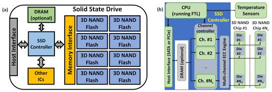
Figure 1.
Layout of the components in an SSD (a) and an overview of its internal architecture (b). Reprinted with permission from [8] under Creative Commons License 4.0 (CC-BY).
From the host standpoint, there are two kinds of data requests, namely write and read. The former gives a freedom degree to the SSD controller in choosing where to physically store the data inside the pool of available 3D NAND Flash chips integrated in the drive. A memory programming operation (i.e., write) features longer latency compared to a read one (1–2 ms versus 75–100 μs [9]); however, since the data to be written can be cached inside DRAM buffers on the SSD the service time (the write QoS) can be reduced [1].
The latter is translated by the SSD controller in a physical 3D NAND Flash address that is exploited in a memory read operation that returns the content of that location the to the host. However, if that address belongs to a device that is already committed in a program operation, the SSD will suffer from prolonged service time and expose large read latency tails [10].
To further complicate the picture, we must remember the 3D NAND Flash characteristics: read and write operation granularity is at the page level (from 4 kB to 16 kB in state-of-the-art devices [11]); however, since the in-place data update operation is prohibited, there is the need of a block erase operation (sized several pages and lasting from 10 ms to 15 ms [9]) that deletes all the invalid data to make room for the updated ones. This free space-reclaim operation, also known as garbage collection (GC) [12,13], can be very long if it encompasses many blocks (several hundreds of milliseconds) and is managed by the SSD controller during the idle times. Read requests can occur during GC, with evident impairment of the QoS in enterprise scenarios where applications rarely provide idle periods. Currently, one of the greatest challenges in the SSD context that must be faced for implementing interactive online services generating thousands of drive accesses [14] is in the experienced read QoS improvement. Either caching techniques or GC preemption cannot provide significant help. A method to handle the QoS-boost shortcoming materializes in the suspension of an ongoing program or an erase operation and the resumption at a later point in time when all prioritized read requests on the memory are serviced [10]. Starting from NAND Flash memory products developed with planar technology [15], vendors provide dedicated commands to suspend the erase operation [14] since this was the one with the highest latency. However, the transition to the 3D counterpart and the increased number of bits stored per cell evidenced that program latency requires suspension as well [9,16].
In this work, we focus on the role of the program operation suspend since we found many unexplored points especially in the design space of 3D NAND Flash-based SSDs. Among them, the operation timing detail and reliability are key features. The former dictates the SSD performance metrics, like the throughput and latency. The latter impacts the error management strategies since the programming operation suspension might alter the memory Raw Bit Error Rate (RBER) metric [17] in non-suspended portions of the memory. Furthermore, since in SSD architectures, there are many 3D NAND Flash devices that are operated simultaneously, the controller must be aware of the potential power consumption surge.
The contributions of this paper are twofold:
- We perform an electrical characterization with respect to the operation timing and reliability on a commercial Triple Level Cell (TLC) 3D NAND Flash technology for enterprise scenarios that includes the program suspend in its command set.
- We evaluate, through a co-simulation framework that accounts for the measured 3D NAND Flash program suspend characteristics, the program suspend’s impact on the figures of merit of an SSD, including the throughput, latency, QoS, and power consumption. Simulations are performed with synthetic benchmarks using different read/write ratios and different micro-architectural drive parameters for design space exploration.
2. Related Works
The interest in developing solutions for preempting long latency operations with shorter ones has been widely explored in the storage scenario. In Reference [18], a new scheduler was proposed to achieve load balancing on the NAND Flash resources of an SSD, thus, granting prioritization mechanisms that may reduce the latency tails. A similar concept was considered in [19] to discuss how read latency fluctuations in Flash-based storage can be reduced using preemptible programs and erases.
Storage technologies different from SSDs also have uses for this topic. In Reference [20], the authors developed a technique for HDDs in which the host input/output transactions are split in small requests to the drive to guarantee the servicing of high priority requests. In Reference [21], the authors studied write cancellation techniques on a non-volatile memory technology with similar NAND Flash characteristics in terms of the read and write latency disparity, namely the Phase Change Memory (PCM) [22].
In addition to those seminal works, specific studies were conducted in the context of the program and erase suspension dynamics either integrating new peripheral circuits in planar NAND Flash devices or at the SSD firmware level. In Reference [14], the authors proposed two practical erase suspension mechanisms and analyzed the trade-offs between the two mechanisms introducing a timeout-based switching policy between the two. A significant reduction in read tail latency is shown on production-grade SSDs. In Reference [10], the first contribution on the program operation suspension appeared; however, its role in isolation with respect to erase was considered only for a few specific cases.
Two strategies for suspension, namely Inter Phase Suspension and Intra Phase Cancellation were proposed showing a direct outcome on SSD read latency. In Reference [23], the authors investigated finer granular read operations for 3D NAND Flash, starting from the circuit-level implementation to memory architecture. Using a novel Single-Operation-Multiple-Location read operation, they can perform several smaller read operations to different locations simultaneously, so that multiple requests can be serviced in parallel. Several patents also dealt with the program suspension topic to be implemented in NAND Flash products [24,25].
All the studies presented so far were focused primary on the steps to implement the operation suspend on Flash storage paradigms that were mostly Single Level Cell (SLC) or Multi Level Cell (MLC). As far as the SSD QoS is concerned, there is an assessment based on the sole read latency without providing additional details concerning the impact of the suspension on the memory reliability and on the SSD’s power consumption. Further, there are no characterization studies concerning 3D NAND Flash products in which the suspension is part of the command set [26] exposed by the memory to the drive.
To the best of our knowledge, this is the first work to investigate the effect of the program operation suspend by characterizing a commercial TLC 3D NAND Flash product integrated in enterprise-class SSD by evaluating the implications on the SSD’s reliability and performance. In this work, we propose general memory-driven design methodologies and algorithms that are functional in the firmware design and can be followed as a general guide for other existing storage products based on 3D NAND Flash.
3. Background and Methods Applied
3.1. 3D NAND Flash Program Suspend
The program operation was implemented in 3D NAND Flash memories by following two consecutive steps: first, the data to be programmed in a specific memory location (i.e., a page) are transferred from the host (in SSDs, the channel controller is responsible for managing this task) and loaded in an on-memory structure called page-buffer [27]; second, an iterative algorithm based on the Incremental Step Pulse Program (ISPP) and verify concept [28] is applied on the target Flash page. In a TLC device, like the one whose structure is depicted in Figure 2a, the data load phase associated to a single wordline of a memory block actually comprises three different page loads in sequence (lower, center, and upper pages) and separated by a setup time (i.e., the page buffer setup time). The ISPP algorithm is then started and ends when all the memory cells in each TLC page reach a desired amount of charge or a threshold voltage (see Figure 2b). The entire program operation lasts several milliseconds as indicated in [9] for state-of-the-art technologies.
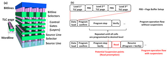
Figure 2.
(a) The TLC 3D NAND Flash architecture. Reprinted with permission from [29] under Creative Commons License 4.0 (CC-BY). (b) An overview of the program operation phase without and with suspension.
Enabling program suspension implies that the ISPP algorithm can be interrupted at any time. The 3D NAND Flash memories assume that the program iteration and verification are a single atomic operation. This is required to avoid the charge loss [30] during the suspension triggering an additional program pulse that could shift the cells to an unwanted threshold voltage level. The resumption from the suspension starts then with a program pulse. The programming voltage before the suspension is stored in the on-chip control logic to avoid the repetition of the same pulse when exiting from the suspension phase [10].
The suspension paradigm dwells in a perfect understanding of the page-buffer role. This on-chip peripheral circuit is shared between the program and the read operation. In the former, it contains the data to be written, and, in the latter, it stores the memory retrieved content from a page before transferring it to the host via the channel controller. Since the controller is responsible for managing all the data transfers to the memory, it can be naively used for storing a copy of the data to write until the program operation is finished.
In the case of a suspension request to preempt a read, it will serve it and then re-send the program data upon program resumption. However, this method performs poorly from the timing standpoint since it overloads the communication resources of the channel controller. In high performance Flash devices, it is embodied a shadow buffer that contains an on-chip replica of the page buffer and that loads itself in the page buffer upon a program request [10].
3.2. Characterization and Simulation Tools
The program suspend operation has been characterized on an off-the-shelf sub-100 layer TLC 3D NAND Flash chip including this feature in its command set. The experimental setup described in [31,32] was exploited in this work. Such an electrical characterization tool interfaces with the memory at a data rate of 400 MT/s and is capable of extracting timing information with 1 μs precision about the on-going program operation by monitoring a dedicated pin of the memory chip (the Ready/Busy pin as the one described in [16]).
The overall program time is the main parameter that we investigated in all the characterizations. As shown in Figure 3a, 3D NAND Flash devices exhibit an intrinsic variability of this parameter. We also performed a measurement to retrieve the inherent variability of by re-programming the same wordline multiple times. Tests demonstrated that, if the number of re-programming cycles was in a range that did not alter the programming characteristics of the wordline, the stayed almost constant. This setup can also extract the number of Fail Bits Count (FBC) on 16 kB pages and, therefore, retrieve reliability information from the memory.
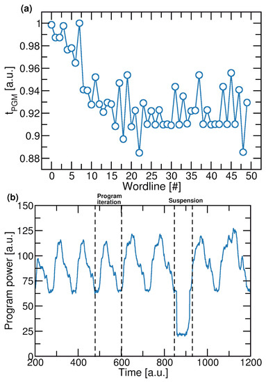
Figure 3.
(a) measurements performed on 50 randomly sampled wordlines in a 3D NAND Flash block. (b) Power consumption measured during a program suspend operation.
Finally, the characterization system exploits two current probes to infer the memory power consumption (at a given supply voltage) from the (i.e., the power supply for the 3D NAND Flash peripheral circuitry) and from the (i.e., the power supply from the memory I/O pins) supplies. For confidentiality reasons, we can only state that is between 2.7 V and 3.6 V, whereas is between 1.2 V and 1.8 V. Figure 3b shows an example (a zoom) of an extracted power trace from a 3D NAND Flash chip during a program suspend operation. In the figure, we can appreciate the single iterations of the program algorithm and the idle consumption during the suspension time since, in this example, no read operations were preempted. As we considered a TLC memory in this study, we collected different power traces for each page type and operation.
To explore the QoS, performance, and power consumption features of SSD architectures integrating 3D NAND Flash memories with program suspend capabilities, we exploited the SSDExplorer co-simulator [33]. The tool allows a fine-grained design space exploration of a drive by allowing modifications of its micro-architectural parameters, including the command queues, interaction mechanisms with the host system, and error recovery policies. The simulations performed considered the 3D NAND Flash timing characteristics as well as the power consumption during the serviced program and read operations through a back annotation process as shown in Figure 4.
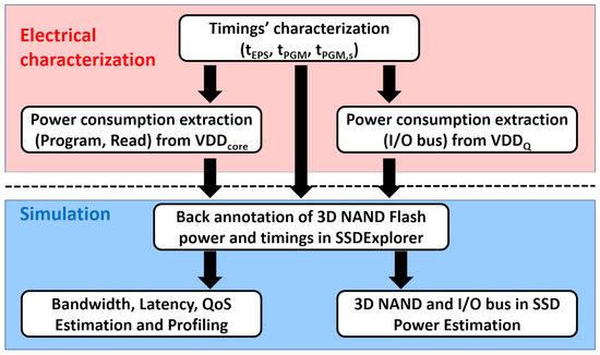
Figure 4.
Electrical characterization of TLC 3D NAND Flash samples and SSD co-simulation flow adopted in this work for the program suspend study.
The assessment of the program suspend role was performed through a microbenchmark that is common in SSDs latency and QoS evaluations [34], namely a 4-kB-aligned workload. A queue depth (QD) either equal to 16 or to 64 was considered with a different mixture of read and write transactions. All the SSD architectural parameters considered in this work are presented in Table 1 and mimic those of an enteprise-class SSD [35].

Table 1.
3D NAND Flash and SSD architectural parameters considered in the simulations.
4. Exploring the Program Suspend in 3D NAND Flash
The assessment of the program suspend characteristics in a TLC 3D NAND Flash product used the test flow depicted in Figure 5. After the reception of the program confirm command, the memory starts the internal program algorithm (e.g., via ISPP) and applies the required program voltage bias to the cells to drive them to the desired threshold voltage level.
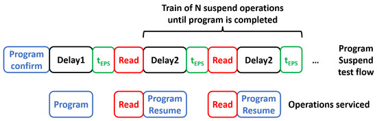
Figure 5.
The program suspend test flow exploited in this work to explore the operation characteristics.
To avoid any topology-related effects that could alter the program characteristics [36], we programmed the TLC pages of the memory with a random pattern. Concurrently, we started a timer (i.e., Delay1) that represented the elapsed time before a read operation should preempt the program in-service. To allow fine-grained exploration, we considered several Delay1 times ranging from 10% up to 100% using 10% steps of the measured without suspension (for confidentiality reasons we cannot report the exact value of the product).
When Delay1 ended, we submitted a program suspend command that was processed by the memory with a time , which represents the time to enter suspend mode. A read operation was then serviced. When all read data were available in the memory page buffer, we resumed the suspended program operation and concurrently started another timer (i.e., Delay2) that represents the elapsed time before servicing another read operation during the program.
Here, we also considered Delay2 times ranging from 10% up to 100% of the . At the end of the Delay2, we were free to service another preempting read operation. This last step involving the Delay2 parameter, as evidenced in Figure 5, was repeated N times until the memory effectively reached the completion of the suspended program operation. This test flow was applied for all Delay1 and Delay2 combinations on 50 different wordlines and TLC pages.
4.1. Number of Suspend Operations
After executing the test flow described thus far, we extracted the actual number of program suspensions that the memory was servicing by exercising all the possible combinations of Delay1 and Delay2. Figure 6 summarizes the results of this characterization. Lower delay times lead to a higher number of suspensions that can be serviced prior the completion of the program operation (up to 10 in our measurements).
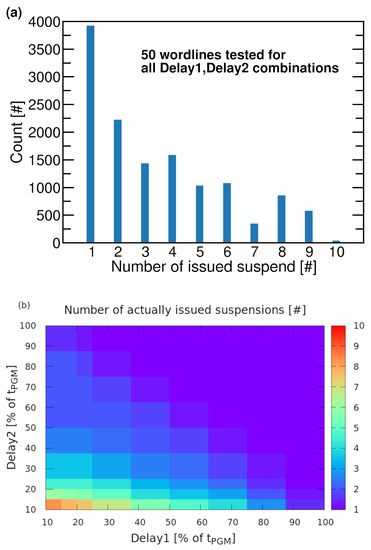
Figure 6.
(a) Histogram of the actual number of issued suspensions considering all the delay combinations and for all 50 wordlines in the study. (b) Number of program suspensions as a function of Delay1 and Delay2.
Interestingly, due to the variability experienced in all the wordlines of a 3D NAND Flash block, there was a slight variability in the number of sustainable program suspensions. If we pick two different wordlines and apply the same delay timing combination in the experiment, we are likely to observe a different number of issued suspend operations due to the different times required to reach the completion of the program phase.
We want to highlight that the results shown in Figure 6 are strongly affected by several factors: (i) the intrinsic variability of the that makes possible for different wordlines to sustain a different number of suspends even when tested with the same Delay1 and Delay2 parameters; and (ii) the small statistics in the overall number of issuable suspends served by the memory. Both factors contribute to a non-monotone decreasing histogram of the number of issued suspend.
As a general rule, we found that, if both Delay1 and Delay2 assume a value higher than 60% of , there is room for servicing only one program suspension.
4.2. Time to Enter in Suspension
The was characterized to assess the impact of the suspend operations on the overall programming time as is the price to pay when a suspend operation is issued. This can be useful in assessing the timings required prior servicing a read operation. We performed two quantifications of the : (i) considering the average value extracted among the 50 tested wordlines in a memory block; and (ii) considering the worst value that also represents the maximum stall time to expect before the read.
The characterization was performed for each combination of the Delay1 and Delay2 values exploited during the tests. Figure 7 demonstrates that, in general, low Delay2 values provide a larger time, although we found some specific combinations of the two delays in which both the average and worst were larger than expected. The magnitude of the was, in general, in a range of few tens of μs, which is 3–4% of the measured without suspensions. That behavior could be ascribed to peculiar 3D NAND Flash internal algorithms in managing the suspension through multiple page buffers.
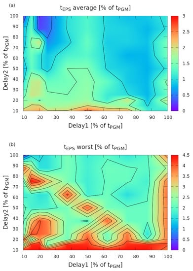
Figure 7.
(a) The average of the measurements performed on 50 randomly sampled wordlines in a 3D NAND Flash block. (b) The worst in each measure.
As speculated in [10], the memory completes the program pulse in the ISPP algorithm independently by the exact point where the user decides to suspend the operation. This is mandatory to avoid the presence of some memory cells in the page to program that receives incomplete pulses and, therefore, has poor control of their program dynamics. The goal is to provide, to all the memory cells, the same ISPP routine even if the iterations in the algorithm are interrupted by the suspension.
4.3. Total Program Time
Suspending the program operation straightforwardly increases the overall program time depending on the number of performed suspensions. Naively, this relationship is assumed to be linear since the higher the suspension number is, the higher the time to complete the program. However, the results previously shown concerning the variability in 3D NAND Flash wordlines and their impact on the number of suspend issued makes this relationship more complex.
Figure 8 shows the results of the characterization performed on the overall program time in the presence of suspensions () achieved through different Delay1 and Delay2 combinations. In general, the number of ISPP iterations for each cell to achieve a desired threshold voltage level is the same with or without suspension (the program dynamics of the cells is not altered by the suspension). Every time we suspend, we have to wait for the time; therefore, the higher the number of suspensions issued is (occurring when the delay timings are low), the larger the overhead on imposed by that metric.
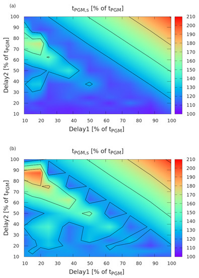
Figure 8.
(a) The average of the overall programming time . (b) The worst extracted from the 50 wordlines involved in the experiment. Both measurements are plotted as a function of different Delay1 and Delay2 combinations.
If both delay timings approach 100% of the , the is more than twice as expected ( is also considered as part of the programming operation since it is time required to enter the suspension mode). However, this result was not achieved for all combinations. We observed that, if Delay1 is relatively small (below 20% of ) and Delay2 is higher than 70% of , we suffer from an increased due to the early described overhead and to an additional combination of factors.
We speculate that, if Delay1 is small (in the range below 20% of ), the memory cells within the wordline we are programming are still in an unstable region of the ISPP algorithm where the relationship between the voltage applied for programming and the threshold voltage of the cells is not linear. For high Delay2 values, an early retention loss of the cells may trigger additional ISPP iterations to reach a target threshold voltage. Both contributions can play a role in the overall increase.
4.4. RBER in Suspended and Not Suspended Blocks
An additional characterization to perform on the program suspend test flow is related to the reliability of the wordlines belonging either to the memory block for which the program is suspended or to other blocks that are not involved by the suspend operation. When the program operation is performed on a specific memory block, all the other blocks in the memory undergo a retention period at a certain temperature (the higher the temperature is, the higher the impact on reliability). The effect of the program suspension is to increase the overall program time of a single page; therefore, we expect that the overall programming time of a block will increase accordingly as well as the retention time experienced by non-programmed blocks.
To better understand, we performed a test in which we programmed, exercising all the possible delay timings combinations, all the wordlines of a memory block. This test induced many program/erase cycles on the same block as, every time we chose a Delay1 and Delay2 combination, we reprogrammed the entire block. We then compared the RBER metric extracted before and after the experiment. At the same time, we extracted the RBER from a randomly chosen block in which no program operations were performed to check whether the program suspension could induce a reliability degradation in other, non-accessed portions of a 3D NAND Flash memory.
As shown in Figure 9a, the program suspension does not alter the reliability characteristics of the wordlines in the block where the operation took place, since the RBER stays the same before and after the experiment. Concerning the wordlines in the memory block (see Figure 9b) for which no programs are executed, we actually see a slight increase of the RBER from the beginning of the experiment; however, this is likely due to the retention loss that we are experiencing at room temperature and is well below the correction limit of the many Error Correction Code engines employed in SSDs [35].
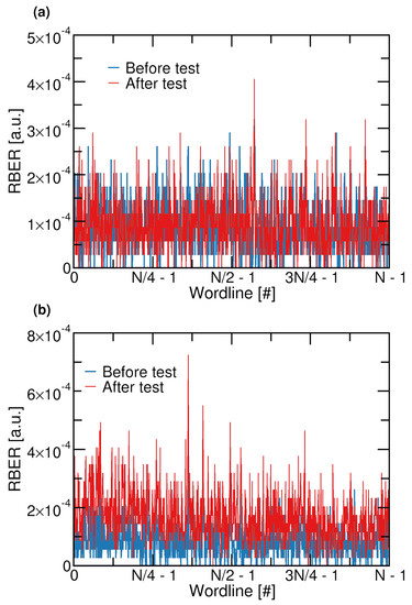
Figure 9.
(a) The RBER measured in all the wordlines of a block where the program suspension took place. (b) The same measurements performed in a block where no program operation is issued.
Based on our experiments, we reached the conclusion that the program suspension did not induce specific reliability issues on the memory with the test conditions adopted. Possible solutions to reduce the RBER in non-suspended blocks could rely on state-of-the-art techniques ranging from advanced Error Correction Code policies (e.g., read retry and soft decoding) or by implementing periodic data refresh strategies to avoid retention-induced charge loss.
5. SSD Simulations to Understand the Role of Program Suspend
We performed a set of SSD simulations using the SSDExplorer platform to understand the impact at the system level of the program suspend operation in 3D NAND Flash memories by back annotating all the electrical characterization metrics presented so far into the simulation environment. As we cannot disclose the full details of the operation timings featured by the tested 3D NAND Flash product, we assume the generic values for the program, read, and erase operations as defined in Table 2, which were extracted from literature referring to a similar TLC 3D NAND Flash technology [9].
Table 2.
The 3D NAND Flash operation timings and voltage intervals considered in the simulations.
The specific values of and shown during the characterization results are taken into account since they are expressed as in terms of relative deviation with respect to , therefore, being applicable in this study case. The workload used as the input stimulus for the SSD to extract all the drive’s performance metrics is either a 75% write −25% read or a 25% write −75% read according to the evaluation guidelines for suspension operations provided in [9].
In all the simulations performed, we compared three different use cases for the SSD: (i) the case in which the 3D NAND Flash memories integrated do not implement the program suspend functionality; (ii) the case where the program suspend is enabled and allows for a maximum of five suspensions to preempt an incoming read operation; and (iii) the same as in the previous case, but allowing up to 10 suspensions.
5.1. SSD Bandwidth and Latency
First, we extracted the achieved SSD’s bandwidth measured in Input/Output operations per second (IOPS). This is a required measurement unit since we are dealing with a random workload. The results of Figure 10a show that the introduction of the program suspend operation increased the sustainable bandwidth irrelevant from the amount of write operations submitted to the drive (i.e., independent from the write/read ratio of the workload).
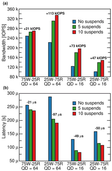
Figure 10.
(a) The SSD bandwidth sustained. (b) The average total latency of the drive. Both metrics are given as a function of the workload and QD.
The higher the number of allowed suspends is, the higher the achieved bandwidth since we are allowing more points in the program operation where the operation can be paused to serve preempting read operations. The biggest advantage in using the suspensions was perceived at high QD values (equal to 64 in our study) and with a workload mostly dominated by the read operations. The achieved bandwidth increase was 113 kIOPS. Such behavior is ascribed to the fact that, in read-intensive workloads, there is a larger pool of preemptible operations and, therefore, enabling program suspension straightforwardly to allocate more servicing time.
The program suspension also provides, as expected from the theoretical standpoint, benefits in terms of the latency experienced by the drive. In Figure 10b, we report the SSD average latency calculated among all the read and write transactions involving the drive. Similarly, as observed earlier, the larger the amount of the allowable suspensions is, the more the experienced latency decreases as well as the performance benefit. For the QD = 64 case, in which the workload is read intensive, there is a latency decrease of 97 μs when up to 10 suspensions are allowed.
5.2. SSD Power Consumption
To understand the role of the program suspension on the SSD’s power consumption, we investigated two different contributions in the drive: (i) the sole 3D NAND Flash memory modules constituting the storage media sub-system; (ii) the internal SSD I/O bus on which both the write and the read flows to and from the memories. As we considered a TLC memory in this study, we collected different power traces for each page type (i.e., lower, central, and upper pages) using our experimental setup applied on a TLC 3D NAND Flash product.
The assumption behind the calculation of the overall memory power consumption in drive is the following: when multiple memory chips are accessed in parallel on an SSD, the Kirchoff’s current law (KCL) holds on the power supply of the drive so that the memory sub-system power consumption is the sum of the single power contributions [8]. The results in Figure 11a show one of the negative sides of the program suspension. When the 3D NAND Flash memories in the SSD allows for preempting read operations, it means that the memory chips are available to sustain more operations per second (as shown by the results in the previous section concerning the bandwidth), hence, being in a sort of “active” state drawing current from the power supply for a longer period.
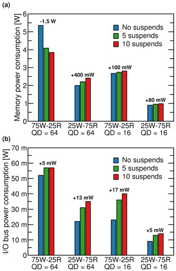
Figure 11.
(a) The power consumption of the memory sub-system in the SSD. (b) The power consumption of the internal I/O bus in the drive.
The larger the number of operations served is, the higher is the power consumption (up to 400 mW increase in the QD = 64 25W-75R condition). A similar result can be appreciated in Figure 11b. Indeed, more suspensions in the program operation means that more read data are to be requested from the memory chips requiring the activation of the internal I/O bus of the drive for a longer period (up to 17 mW in the QD = 16 75W-25R condition).
The only counter-intuitive result is related to the power consumption extracted from simulations with a write intensive workload and QD = 64, in which the former metric displays an inverted trend with respect to all the other cases. We interpret this result as a combination of several factors. The case of QD = 64 represents a situation in which all the SSD resources (i.e., channels) are allocated to serve write/read transactions.
Write (program) operations in 3D NAND Flash devices consume more power than the read one, and, since the former operation is longer, there is a large probability, especially in the high QD scenario, that multiple 3D NAND Flash chips concurrently serve a write function, and therefore the total power consumption is the sum of each operation. By including program suspensions, we are deliberately reducing that probability and allowing a power consumption reduction of almost 1.5 W.
5.3. The Impact on QoS
The QoS study can be performed in multiple ways since it depends on the definition of the QoS level and on the latency that is being profiled for reaching that. In this study, we considered, without a lack of generality, a QoS calculated at the 99.99% percentile of the latency Cumulative Distribution Function (CDF) [32] either considering the total transactions sustained by the drive (i.e., total QoS) or only considering the read transactions (i.e., read QoS), which are those benefiting from the program suspension. Figure 12 shows a profile of a latency CDF in which the read, write, and total contributions of the QoS are appreciable.
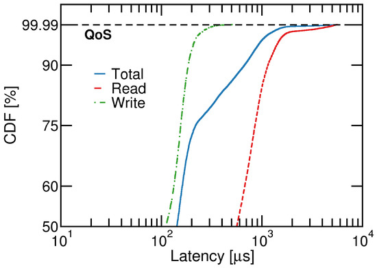
Figure 12.
The latency CDF profile of a 75W-25R workload with QD = 64 simulated with the SSDExplorer framework.
Figure 13a shows that the total QoS performed 630 μs better when the program suspension was exploited in workloads largely dominated by read operations that were prioritized with respect to write. Workloads performed on lower QD values still displayed an advantage even if it became marginal (i.e., a few hundred μs). Increasing the number of allowable suspensions from 5 to 10 slightly penalized the QoS, but in the high QD scenario there was still a large advantage compared with the no supensions case. Similar considerations can be extrapolated from the results of the read QoS shown in Figure 13b; however, here, the QoS gain increased up to 1.03 ms, proving that the program suspension is one of the most suitable ways to reduce the latency in read intensive scenarios.
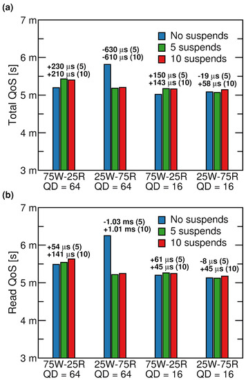
Figure 13.
(a) The total QoS. (b) The read QoS. Both metrics were extracted at the 99.99-percentile of the latency CDF.
6. Conclusions
In this work, we assessed the role of the program suspend operation in TLC 3D NAND Flash memories envisioned as the storage medium of SSDs platforms. The electrical characterization performed on an off-the-shelf product demonstrated that the overall program time, including the suspension and the time required to enter in the suspension phase, was not a linear function of the wait time before the arrival of a preempting read operation. We also observed that the impact on the memory RBER in suspended and non-suspended blocks was negligible, therefore, proving the safe applicability of the suspend paradigm.
By back annotating the timing and the power consumption features of the product in the SSDExplorer co-simulation environment, we were able to run a design space exploration using different workloads and micro-architectural parameters, such as the QD. The simulation results demonstrated that the program suspend led to a 113 kIOPS increase in terms of the achieved drive’s bandwidth and an average latency reduction of 97 μs.
Finally, we exposed the drawbacks of the program suspend operation in terms of the SSD power consumption, and we observed that the real advantage on the QoS (1.03 ms) was appreciable mainly in read intensive scenarios at a high QD range.
Author Contributions
The individual contributions to this paper are the following: conceptualization, C.Z. and R.M.; methodology, C.Z. and R.M.; software, L.Z.; validation, C.Z., L.Z. and R.M.; electrical measurements and resources, A.A. and S.S.; investigation, C.Z., L.Z., A.A. and R.M.; data curation, C.Z. and R.M.; writing—original draft preparation, C.Z. and R.M.; writing—review and editing, R.M. and P.O.; visualization, C.Z.; supervision, R.M. and P.O. All authors have read and agreed to the published version of the manuscript.
Funding
This research received no external funding.
Conflicts of Interest
The authors declare no conflict of interest.
Abbreviations
The following abbreviations are used in this manuscript:
| GC | Garbage Collection |
| HDD | Hard Disk Drive |
| HPC | High Performance Computing |
| IOPS | Input/Output Operations Per Second |
| MLC | Multi Level Cell |
| QD | Queue Depth |
| QoS | Quality of Service |
| RBER | Raw Bit Error Rate |
| SLC | Single Level Cell |
| SSD | Solid State Drive |
| TLC | Triple Level Cell |
References
- Zuolo, L.; Zambelli, C.; Micheloni, R.; Olivo, P. Solid-State Drives: Memory Driven Design Methodologies for Optimal Performance. Proc. IEEE 2017, 105, 1589–1608. [Google Scholar] [CrossRef]
- Schroeder, B.; Merchant, A.; Lagisetty, R. Reliability of nand-Based SSDs: What Field Studies Tell Us. Proc. IEEE 2017, 105, 1751–1769. [Google Scholar] [CrossRef]
- Zuolo, L.; Zambelli, C.; Micheloni, R.; Bertozzi, D.; Olivo, P. Analysis of reliability/performance trade-off in Solid State Drives. In Proceedings of the IEEE International Reliability Physics Symposium (IRPS), Waikoloa, HI, USA, 1–5 June 2014; pp. 4B.3.1–4B.3.5. [Google Scholar] [CrossRef]
- SNIA—Solid State Storage Initiative. An Introduction to Solid State Drive Performance, Evaluation and Test. 2013. Available online: https://www.snia.org/sites/default/files/SNIASSSI.SSDPerformance-APrimer2013.pdf (accessed on 21 April 2021).
- Grossi, A.; Zuolo, L.; Restuccia, F.; Zambelli, C.; Olivo, P. Quality-of-Service Implications of Enhanced Program Algorithms for Charge-Trapping NAND in Future Solid-State Drives. IEEE Trans. Device Mater. Reliab. 2015, 15, 363–369. [Google Scholar] [CrossRef]
- Gugnani, S.; Lu, X.; Panda, D.K. Analyzing, Modeling, and Provisioning QoS for NVMe SSDs. In Proceedings of the IEEE/ACM 11th International Conference on Utility and Cloud Computing (UCC), Zurich, Switzerland, 17–20 December 2018; pp. 247–256. [Google Scholar] [CrossRef]
- Sun, C.; Le Moal, D.; Wang, Q.; Mateescu, R.; Blagojevic, F.; Lueker-Boden, M.; Guyot, C.; Bandic, Z.; Vucinic, D. Latency Tails of Byte-Addressable Non-Volatile Memories in Systems. In Proceedings of the IEEE International Memory Workshop (IMW), Monterey, CA, USA, 14–17 May 2017; pp. 1–4. [Google Scholar] [CrossRef]
- Zambelli, C.; Zuolo, L.; Crippa, L.; Micheloni, R.; Olivo, P. Mitigating Self-Heating in Solid State Drives for Industrial Internet-of-Things Edge Gateways. Electronics 2020, 9, 1179. [Google Scholar] [CrossRef]
- Pletka, R.; Papandreou, N.; Stoica, R.; Pozidis, H.; Ioannou, N.; Fisher, T.; Fry, A.; Ingram, K.; Walls, A. Achieving Latency and Reliability Targets with QLC in Enterprise Controllers. In Proceedings of the Flash Memory Summit, Santa Clara, CA, USA, 10–12 November 2020. [Google Scholar]
- Wu, G.; He, X. Reducing SSD Read Latency via NAND Flash Program and Erase Suspension. In Proceedings of the USENIX Conference on File and Storage Technologies, San Jose, CA, USA, 14 February 2012; pp. 1–10. [Google Scholar] [CrossRef]
- Micheloni, R.; Aritome, S.; Crippa, L. Array Architectures for 3-D NAND Flash Memories. Proc. IEEE 2017, 105, 1634–1649. [Google Scholar] [CrossRef]
- Yamada, T.; Sun, C.; Takeuchi, K. A high-performance solid-state drive by garbage collection overhead suppression. In Proceedings of the Non-Volatile Memory Technology Symposium (NVMTS), Jeju, Korea, 27–29 October 2014; pp. 1–2. [Google Scholar] [CrossRef]
- Shin, W.; Kim, M.; Kim, K.; Yeom, H.Y. Providing QoS through host controlled flash SSD garbage collection and multiple SSDs. In Proceedings of the International Conference on Big Data and Smart Computing (BIGCOMP), Jeju, Korea, 9–11 February 2015; pp. 111–117. [Google Scholar] [CrossRef]
- Kim, S.; Bae, J.; Jang, H.; Jin, W.; Gong, J.; Lee, S.; Ham, T.J.; Lee, J.W. Practical Erase Suspension for Modern Low-Latency SSDs. In Proceedings of the USENIX Conference on Usenix Annual Technical Conference, Renton, WA, USA, 10 July 2019; pp. 813–820. [Google Scholar] [CrossRef]
- Li, Y. 3 Bit Per Cell NAND Flash Memory on 19nm Technology. In Proceedings of the Flash Memory Summit, San Jose, CA, USA, 22–24 August 2012. [Google Scholar]
- Maejima, H.; Kanda, K.; Fujimura, S.; Takagiwa, T.; Ozawa, S.; Sato, J.; Shindo, Y.; Sato, M.; Kanagawa, N.; Musha, J.; et al. A 512Gb 3b/Cell 3D flash memory on a 96-word-line-layer technology. In Proceedings of the IEEE International Solid-State Circuits Conference (ISSCC), San Francisco, CA, USA, 11–15 February 2018; pp. 336–338. [Google Scholar] [CrossRef]
- Mielke, N.R.; Frickey, R.E.; Kalastirsky, I.; Quan, M.; Ustinov, D.; Vasudevan, V.J. Reliability of Solid-State Drives Based on NAND Flash Memory. Proc. IEEE 2017, 105, 1725–1750. [Google Scholar] [CrossRef]
- Elyasi, N.; Arjomand, M.; Sivasubramaniam, A.; Kandemir, M.T.; Das, C.R.; Jung, M. Exploiting Intra-Request Slack to Improve SSD Performance. SIGPLAN Not. 2017, 52, 375–388. [Google Scholar] [CrossRef]
- Park, J.; Lee, J.; Kim, M.; Chun, M.; Kim, J. Reducing read latency fluctuations of flash storage systems using preemptible programs and erases. In Proceedings of the Conference on File and Storage Technologies, Work-in-Progress Reports (WiPs), FAST’18. USENIX Association, Oakland, CA, USA, 12–15 February 2018. [Google Scholar]
- Dimitrijevic, Z.; Rangaswami, R. Design and Implementation of Semi-preemptible IO. In Proceedings of the Conference on File and Storage Technologies—FAST, San Francisco, CA, USA, 31 March–2 April 2003. [Google Scholar]
- Qureshi, M.K.; Franceschini, M.M.; Lastras-Montaño, L.A. Improving read performance of Phase Change Memories via Write Cancellation and Write Pausing. In Proceedings of the International Symposium on High-Performance Computer Architecture (HPCA), Bangalore, India, 9–14 January 2010; pp. 1–11. [Google Scholar] [CrossRef]
- Zambelli, C.; Navarro, G.; Sousa, V.; Prejbeanu, I.L.; Perniola, L. Phase Change and Magnetic Memories for Solid-State Drive Applications. Proc. IEEE 2017, 105, 1790–1811. [Google Scholar] [CrossRef]
- Liu, C.Y.; Kotra, J.B.; Jung, M.; Kandemir, M.T.; Das, C.R. SOML Read: Rethinking the Read Operation Granularity of 3D NAND SSDs. In Proceedings of the International Conference on Architectural Support for Programming Languages and Operating Systems (ASPLOS), Providence, RI, USA, 13–17 April 2019; pp. 955–969. [Google Scholar] [CrossRef]
- Hyun, J.W.; Brinicombe, M.; Sun, H.; Zhong, H.; Strasser, J.; Wood, R. Program Suspend/Resume for Memory. U.S. Patent 9021158B2, 2015. Available online: https://patents.google.com/patent/US9021158B2/en (accessed on 2 May 2021).
- Micheloni, R.; Aldarese, A.; Scommegna, S. Method and Apparatus with Program Suspend Using Test Mode. U.S. Patent 9892794B2, 2018. Available online: https://patents.google.com/patent/US9892794B2/en (accessed on 2 May 2021).
- Bjorling, M. Open-Channel Solid State Drives NVMe Specification (rev 1.2). 2018. Available online: http://lightnvm.io/docs/OCSSD-2_0-20180129.pdf (accessed on 23 April 2021).
- Takeuchi, K.; Tanaka, T. A dual-page programming scheme for high-speed multigigabit-scale NAND flash memories. IEEE J. Solid-State Circ. 2001, 36, 744–751. [Google Scholar] [CrossRef]
- Suh, K.D.; Suh, B.H.; Um, Y.H.; Kim, J.K.; Choi, Y.J.; Koh, Y.N.; Lee, S.S.; Kwon, S.C.; Choi, B.S.; Yum, J.S.; et al. A 3.3 V 32 Mb NAND flash memory with incremental step pulse programming scheme. In Proceedings of the International Solid-State Circuits Conference, San Francisco, CA, USA, 15–17 February 1995; pp. 128–129. [Google Scholar] [CrossRef]
- Zambelli, C.; Micheloni, R.; Scommegna, S.; Olivo, P. First Evidence of Temporary Read Errors in TLC 3D-NAND Flash Memories Exiting From an Idle State. IEEE J. Electron Devices Soc. 2020, 8, 99–104. [Google Scholar] [CrossRef]
- Chen, C.P.; Lue, H.T.; Hsieh, C.C.; Chang, K.P.; Hsieh, K.Y.; Lu, C.Y. Study of fast initial charge loss and it’s impact on the programmed states Vt distribution of charge-trapping NAND Flash. In Proceedings of the International Electron Devices Meeting (IEDM), San Francisco, CA, USA, 6–8 December 2010; pp. 5.6.1–5.6.4. [Google Scholar] [CrossRef]
- Zambelli, C.; King, P.; Olivo, P.; Crippa, L.; Micheloni, R. Power-supply impact on the reliability of mid-1X TLC NAND flash memories. In Proceedings of the IEEE International Reliability Physics Symposium (IRPS), Pasadena, CA, USA, 17–21 April 2016; pp. 2B-3-1–2B-3-6. [Google Scholar] [CrossRef]
- Zambelli, C.; Micheloni, R.; Crippa, L.; Zuolo, L.; Olivo, P. Impact of the NAND Flash Power Supply on Solid State Drives Reliability and Performance. IEEE Trans. Device Mater. Reliab. 2018, 18, 247–255. [Google Scholar] [CrossRef]
- Zuolo, L.; Zambelli, C.; Micheloni, R.; Indaco, M.; Carlo, S.D.; Prinetto, P.; Bertozzi, D.; Olivo, P. SSDExplorer: A Virtual Platform for Performance/Reliability-Oriented Fine-Grained Design Space Exploration of Solid State Drives. IEEE Trans. Comput. Aided Des. Integr. Circ. Syst. 2015, 34, 1627–1638. [Google Scholar] [CrossRef]
- Hady, F.T.; Foong, A.; Veal, B.; Williams, D. Platform Storage Performance With 3D XPoint Technology. Proc. IEEE 2017, 105, 1822–1833. [Google Scholar] [CrossRef]
- Microsemi PM8609 NVMe2032 Flashtec NVMe Controller. 2019. Available online: https://www.microsemi.com/product-directory/storage-ics/3687-flashtec-nvme-controllers (accessed on 2 May 2021).
- Monzio Compagnoni, C.; Ghetti, A.; Ghidotti, M.; Spinelli, A.S.; Visconti, A. Data Retention and Program/Erase Sensitivity to the Array Background Pattern in Deca-nanometer nand Flash Memories. IEEE Trans. Electron Devices 2010, 57, 321–327. [Google Scholar] [CrossRef]
Publisher’s Note: MDPI stays neutral with regard to jurisdictional claims in published maps and institutional affiliations. |
© 2021 by the authors. Licensee MDPI, Basel, Switzerland. This article is an open access article distributed under the terms and conditions of the Creative Commons Attribution (CC BY) license (https://creativecommons.org/licenses/by/4.0/).