Article

A New Simulated Inductor with Reduced Series Resistor Using a Single VCII±

1
Department of Electrical and Electronics Engineering, Pamukkale University, Denizli 20160, Turkey
2
Department of Industrial and Information Engineering, University of L’Aquila, 67100 L’Aquila, Italy
3
Department of Electrical and Electronics Engineering, Dogus University, Istanbul 34775, Turkey
*
Author to whom correspondence should be addressed.
Electronics 2021, 10(14), 1693; https://doi.org/10.3390/electronics10141693
Submission received: 10 June 2021 / Revised: 8 July 2021 / Accepted: 12 July 2021 / Published: 15 July 2021
(This article belongs to the Section Circuit and Signal Processing)

Abstract

:
This paper presents a new realization of a grounded simulated inductor using a single dual output second-generation voltage conveyor (VCII±) as an active building block, two resistors and one grounded capacitor. The main characteristic of the proposed circuit is that the value of the series resistor can be significantly reduced. Thus, it has the property of improved low-frequency performance. Another feature is the use of a grounded capacitor that makes the proposed circuit attractive for integrated circuit (IC) realization. A simple CMOS implementation of the required VCII± is used. However, a single passive component-matching condition is required for the proposed structure. As an application example, a standard fifth-order high-pass ladder filter is also given. SPICE simulations using 0.18 μm CMOS technology parameters and a supply voltage of ±0.9 V as well as experimental verifications, are carried out to support the theory.

1. Introduction

Inductors are analog passive components that play an essential role in many analog and mixed-signal circuits. Due to the large occupation of area and the low-quality factor of spiral inductors, designers prefer to substitute them with simulated inductors (SIs) [1,2,3,4,5,6,7,8,9,10,11,12,13,14,15,16,17,18,19,20,21,22,23,24,25,26,27,28,29,30,31,32,33,34,35,36,37,38,39,40,41,42,43,44,45,46,47,48,49]. SIs are constructed using a few active elements, resistors and one capacitor, and exhibit characteristics of inductance within a specified frequency range. They find wide applications in the design of active filters, oscillators, phase shifters, etc. SIs using various kind of active devices offer some advantages such as the capability for integration, low area, high quality factor, operation in a wide frequency range, etc. However, grounded SIs [1,2,3,4,5,6,7,8,9,10,11,12,13,14,15,16,17,18,19,20,21,22,23,24,25,26,27,28,29,30,31,32,33,34,35,36,37,38,39,40,41,42,43,44,45,46,47,48,49] have the following problems. Some of the grounded SIs [1,2] use operational amplifiers (OAs); therefore, they suffer from slew-rate limitations. Other grounded SIs [1,2,3,4,5,6,7,8,9,10,12,13,14,19,21,31,33,34,39,48,49] employ more than one active building block (ABB). The grounded SI configurations described in [1,2,6,11,12,15,16,17,18,19,20,24,25,26,27,28,35,37,39,43,44,45,46,47] include a floating capacitor that is not suitable for integrated circuit (IC) fabrication. The grounded SI proposals in [17,22,24,25,26,27,28,29,30,36,38,42,45,46] contain complex internal structures. Other grounded topologies [40,41,42,43,44,45,46] are made up of non-standard active devices. Finally, the grounded SI architectures reported in [9,23,30,31,32,33,34,35,37] have a capacitor connected to a low-impedance terminal or consist of an operational transconductance amplifier (OTA); accordingly, their high-frequency performances are limited [50,51].
A literature survey revealed that, in recent years, the current-mode (CM) approach has been widely used in the SI design [1,2,3,4,5,6,7,8,9,10,11,12,13,14,15,16,17,20,21,22,24,25,26,27,28,29,36,38,39,40,41,42,43,44,45,46,47,48,49]. The main reason is the potential of the CM signal processing with its low-voltage nature and high-frequency operation, etc. [52,53]. Recently, a new CM active building block called second-generation voltage conveyor (VCII) [54,55,56] has been used in the implementation of high-performance grounded immittance-function simulators [48,57]. This new block is the dual circuit of the more famous second-generation current conveyor (CCII). The difference between CCII and VCII is that, unlike VCII, CCII lacks a low-impedance voltage output port. This feature enables VCII-based circuits to benefit from advantages of processing signals in the current domain while producing output signals in voltage form. Therefore, VCII is suitable for all applications requiring output signal in the form of voltage. The results reported in [54,55,56] reveal that VCII-based circuits outperform conventional circuits in many aspects. For instance, achieved simulated impedances in [48,57] are robust against process mismatches and temperature variations while their power consumption is reduced, when compared to the other reported work. The latter feature comes from the very simple internal structure of the used ABB, i.e., VCII. The maximum operation frequency range and parasitic series impedance of the VCII-based grounded SI reported in [48] are 2.5 MHz and 191 Ω, respectively. It also employs two ABBs.
Here, we aim to design a VCII-based grounded SI with improved performance that uses only one ABB. The proposed circuit is based on one dual-output VCII (VCII±) as ABB, two resistors and one grounded capacitor. The most important feature of the new implementation is that the value of series impedance is considerably reduced by adjusting resistor values. Hence, it has the property of improved low-frequency performance. It employs only a grounded capacitor that results in easy integration in the IC process. In addition, the frequency range is extended to 10 MHz. Additionally, complete circuit analysis and SPICE simulation results are reported. As an application example, a fifth-order high-pass (HP) ladder filter is presented. Nevertheless, there is a simple matching condition which can be easily satisfied. Fortunately, this matching condition is also useful in setting the value of parasitic series resistance to the desired value. The promising results through the SPICE simulation program and experimental verifications show that VCIIs are highly suitable in the SI applications. Compared to the grounded SI based on the negative-impedance converters (NICs) of [49] which employ two active elements, two resistors and one grounded capacitor, the realized inductor value is four times lower than the one extracted from the proposed circuit for the same values of the capacitor and resistors.
The organization of this paper is as follows. In Section 2, VCII± and the proposed SI are introduced and analyzed. The non-ideal analysis is performed in Section 3. Simulation results are reported in Section 4. Experimental verifications are presented in Section 5. Finally, Section 6 concludes the paper.

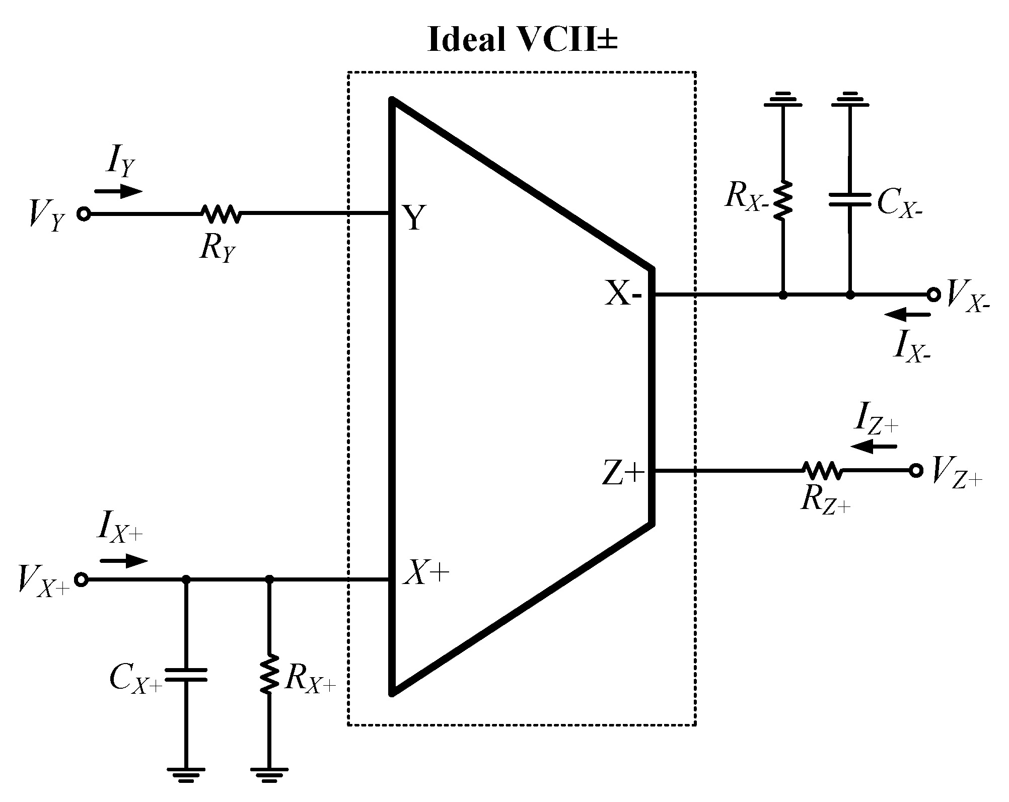
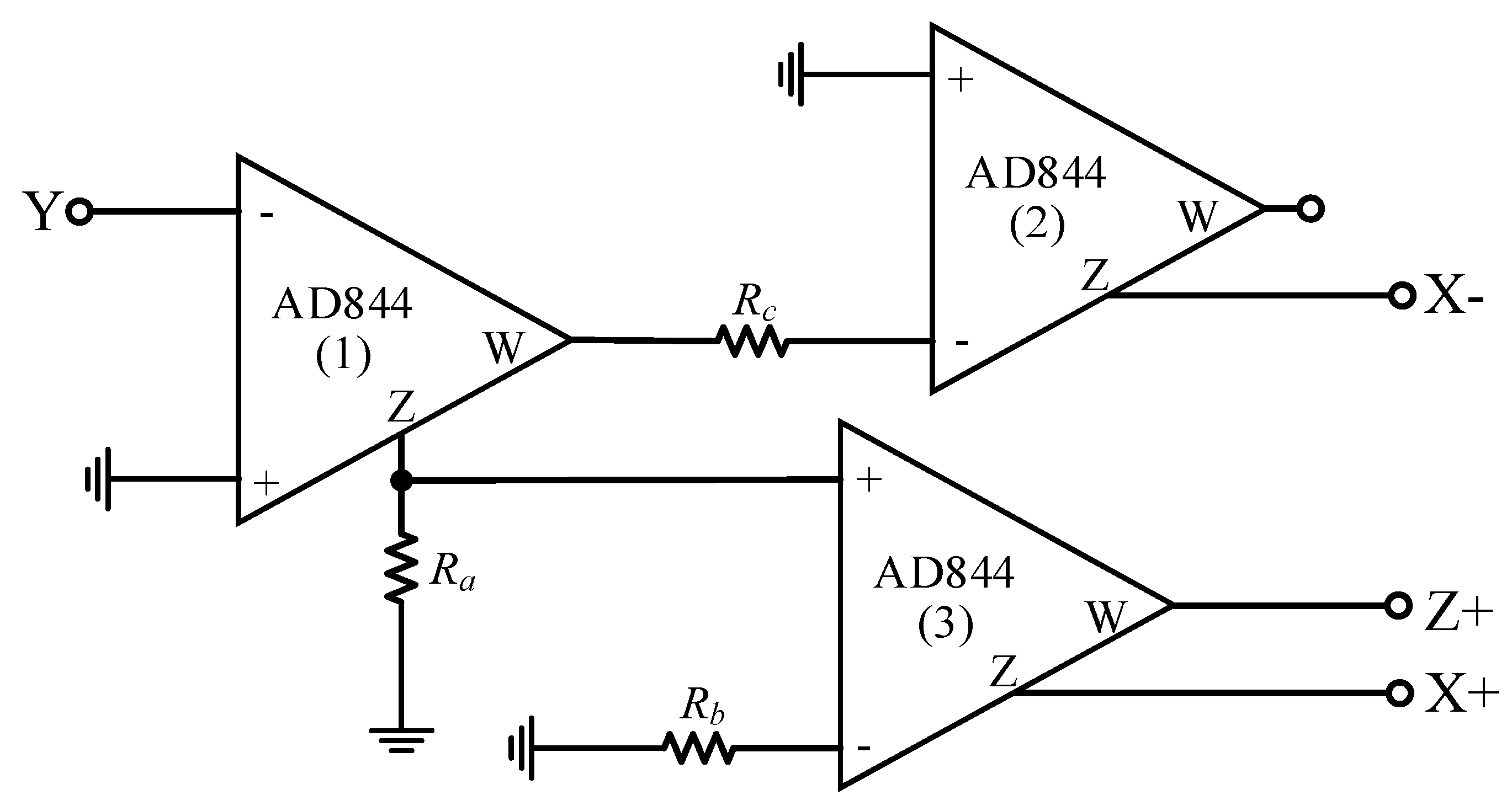
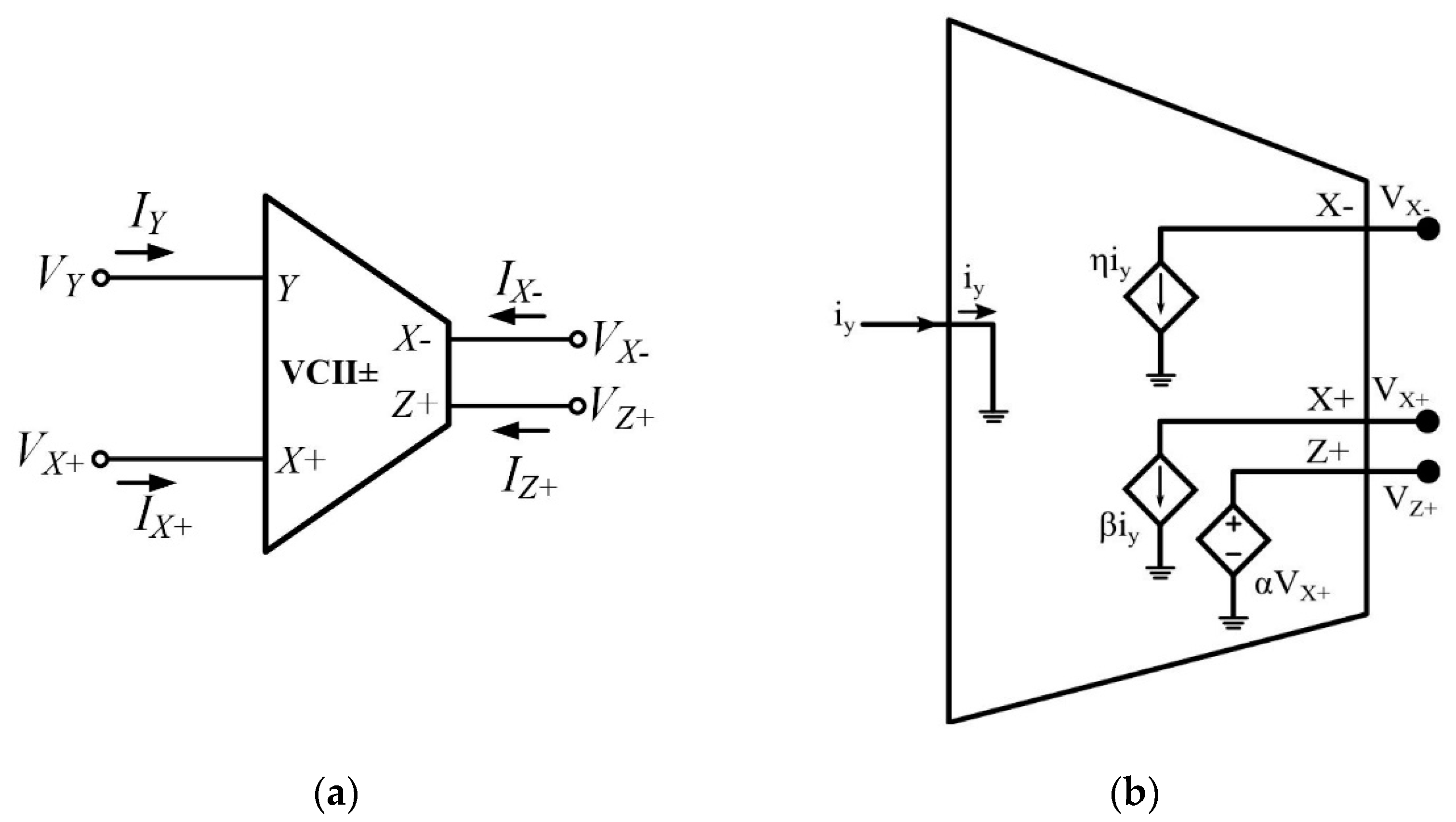
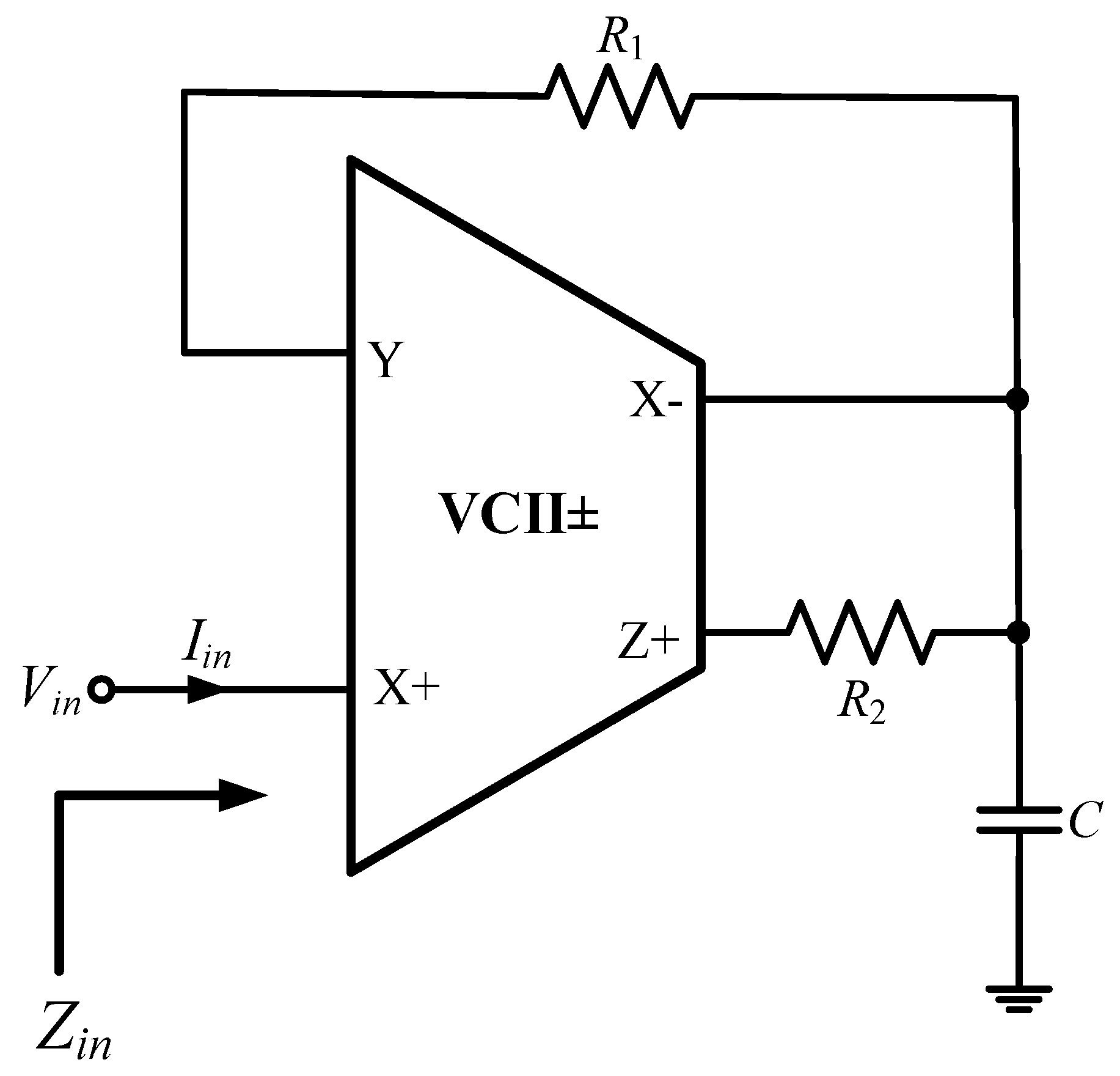
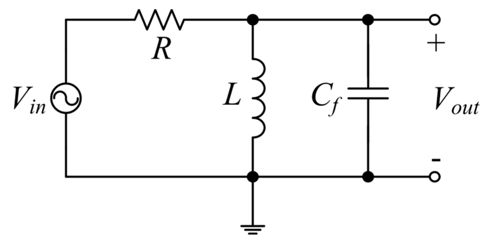
2. The Proposed Circuit

Figure 1 shows the symbolic presentation and internal structure of the VCII± without a Z− port. It has a low-impedance current input Y terminal, two high-impedance current output X+ and X− terminals and one low impedance voltage output terminal, Z+. It simply consists of a current buffer (CB) and a voltage buffer (VB). The input current is transferred from the Y terminal to the X+ terminal in the same direction and the X− terminal in the opposite direction. The voltage at the X+ terminal is transferred to the Z+ terminal. The VCII± demonstrated in Figure 1 is described as:
[ I X + I X V Y V Z + ] = [ 0 0 β 0 0 η 0 α 0 0 0 0 ] [ V X + V X I Y ]
In Equation (1), β and η, being current gains, are ideally equal to one and two, respectively. Additionally, α, being voltage gain, is ideally equal to unity.
The proposed VCII±-based SI is shown in Figure 2. Simple analysis shows that, in the case of ideal VCII (negligible contribution of parasitic impedances), the input impedance of the proposed SI is evaluated by
Z i n ( s ) = s C R 1 R 2 + R 1 R 2
In above equation, if R2 = R1 = R is chosen, the following input impedance is obtained:
Z i n ( s ) = s C R 2
One observes from Equation (3) that a positive lossless grounded SI is obtained. If non-ideal gains are considered, Equation (2) turns to:
Z i n ( s ) = s C R 1 R 2 + R 1 + ( 1 η ) R 2 α β
From Equation (4), quality factor (Q) for equivalent inductance is found as
Q = | ω C R 1 R 2 R 1 + ( 1 η ) R 2 |
From Equation (5) it can be realized that for the ideal case, where R1 = R2 and η = 2, the Q value of the inductance is infinity.

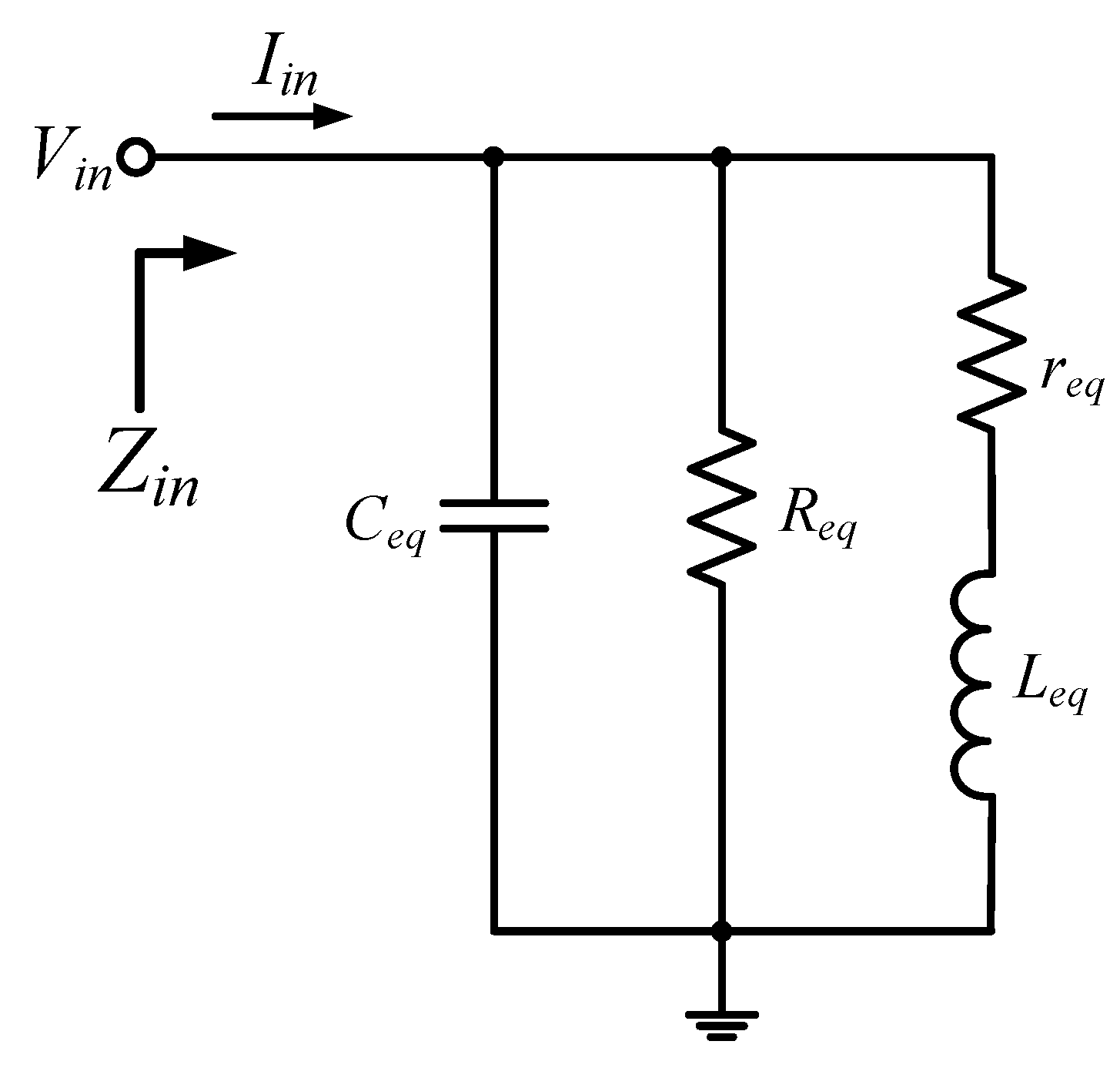
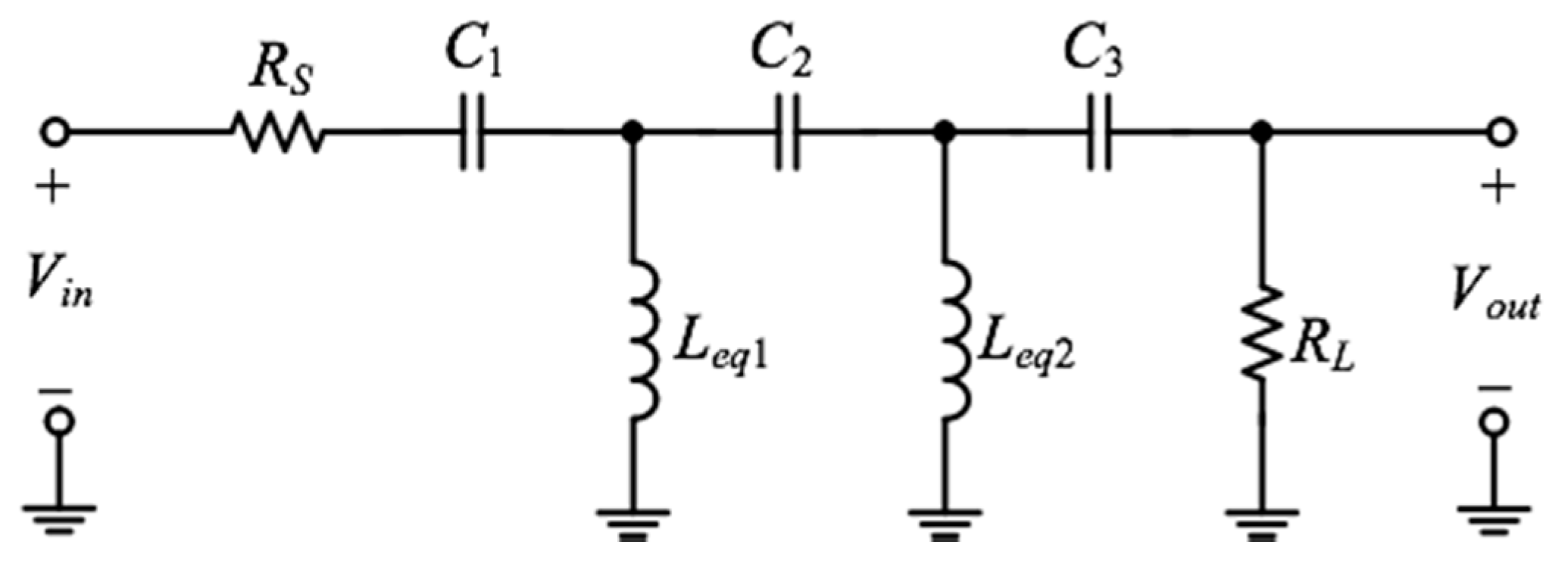
3. Parasitic Impedance Effects

Figure 3 and Figure 4 show the VCII± with its parasitic impedances and the equivalent model of the proposed SI, respectively. Thus, the VCII± denoted in Figure 3 is described as
[ I X + I X V Y V Z + ] = [ s C x + + 1 R X + 0 1 0 0 s C x + 1 R X 2 0 0 1 0 0 R Y 0 0 R Z + ] [ V X + V X I Y I Z + ]
By a simple analysis, including only parasitic impedances of the VCII±, Equation (2) converts to:
Z i n ( s ) = R e q / / 1 s C e q / / ( s L e q + r e q )
Here, Leq, req, Req and Ceq are, respectively, calculated as
L e q = ( C + C X ) ( R 1 + R Y ) ( R 2 + R Z + )
r e q = ( R 1 + R Y ) + ( R 2 + R Z + ) R X + R 1 + R Y R 2 R Z +
R e q = R X +
C e q = C X +
It is seen from Equations (7) and (8) that the proposed SI has restrictions at high frequencies due to parasitic elements RX+ and CX+ and at low frequencies due to req. Fortunately, req can be set to zero by choosing R2 as follows:
R 2 = ( R 1 + R Y ) R Z + + ( R 1 + R Y R Z + ) R X R X ( R 1 + R Y )
If RX− is too high (RX− > ∞), the Equation (12) is reduced to R2 = R1 + RYRZ+, which is easily satisfied in practice.

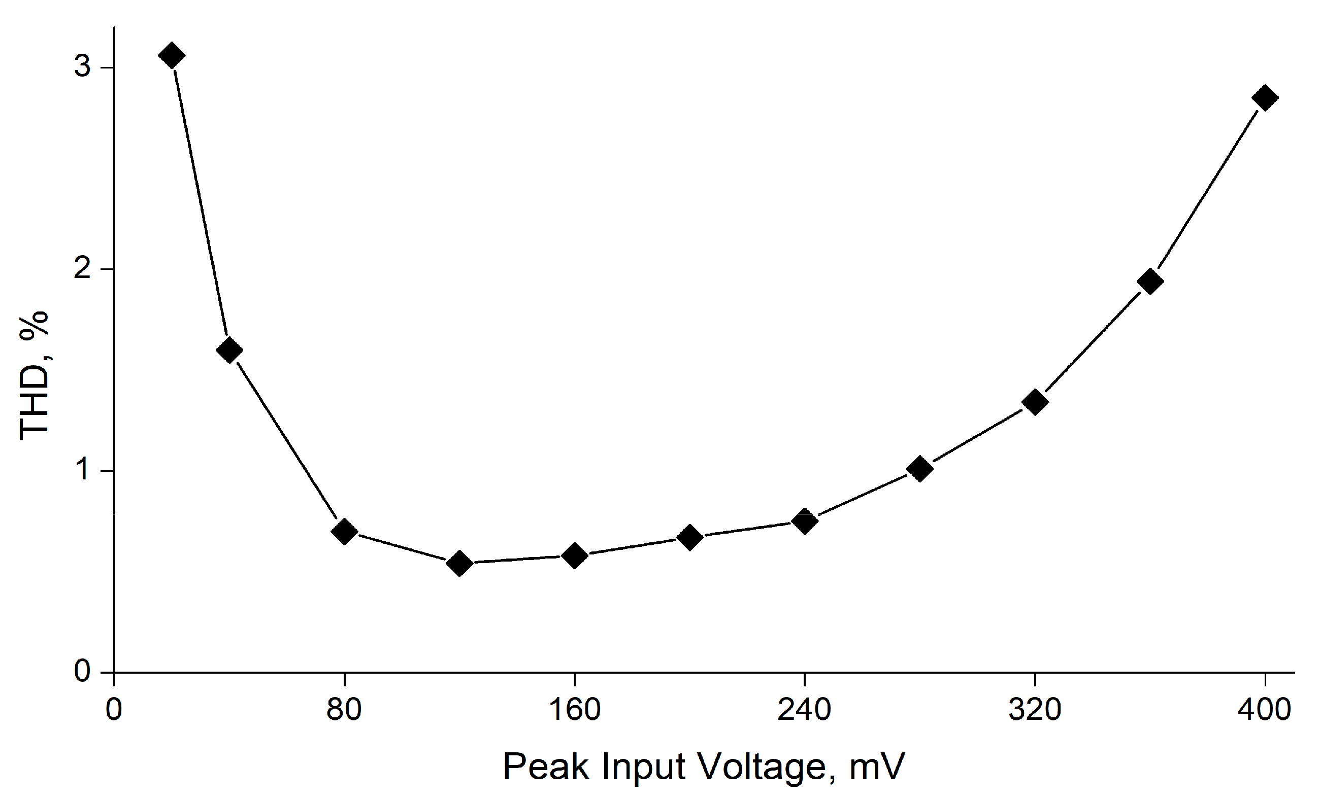
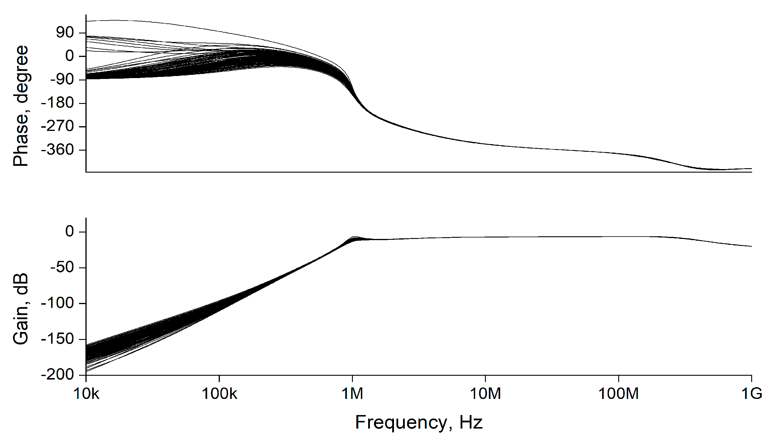
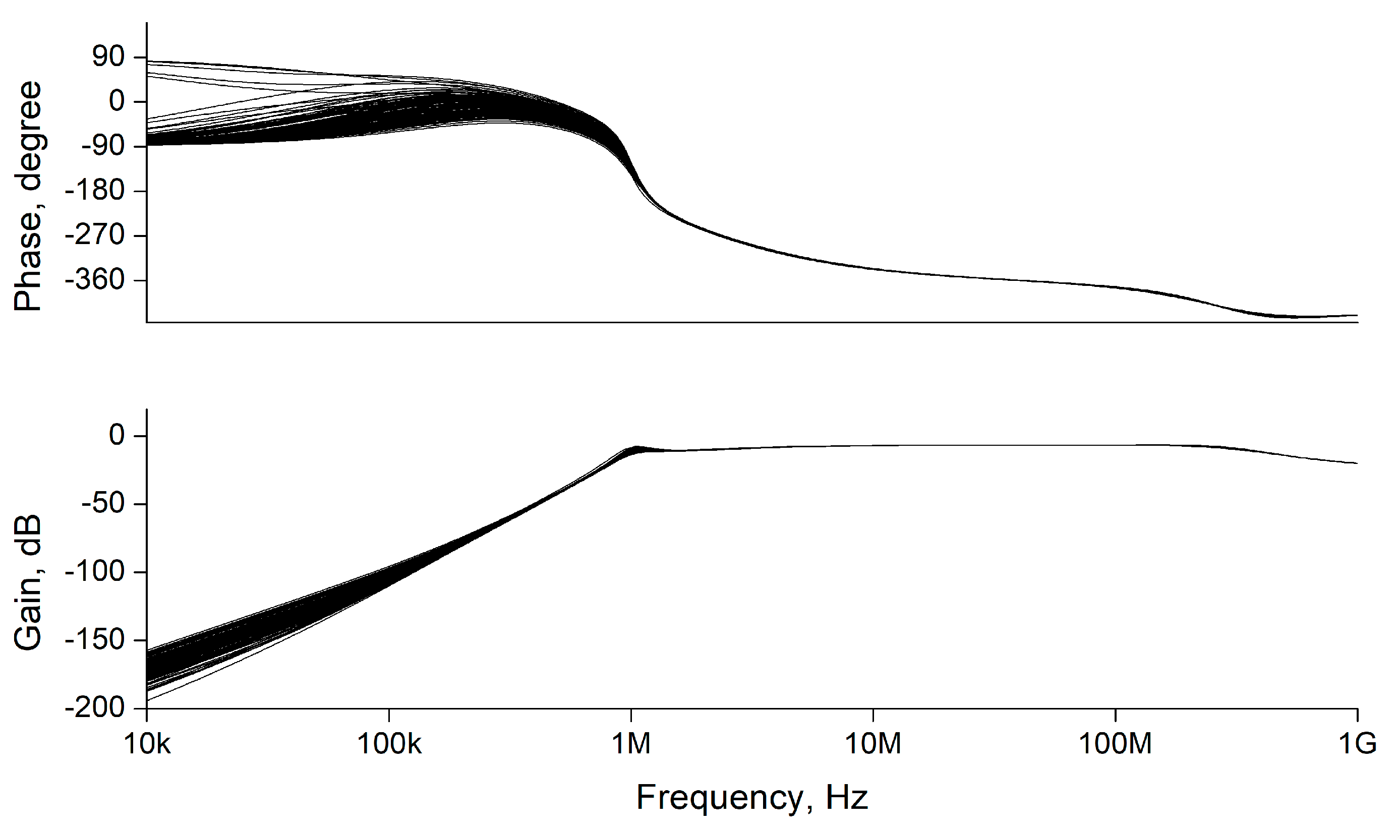
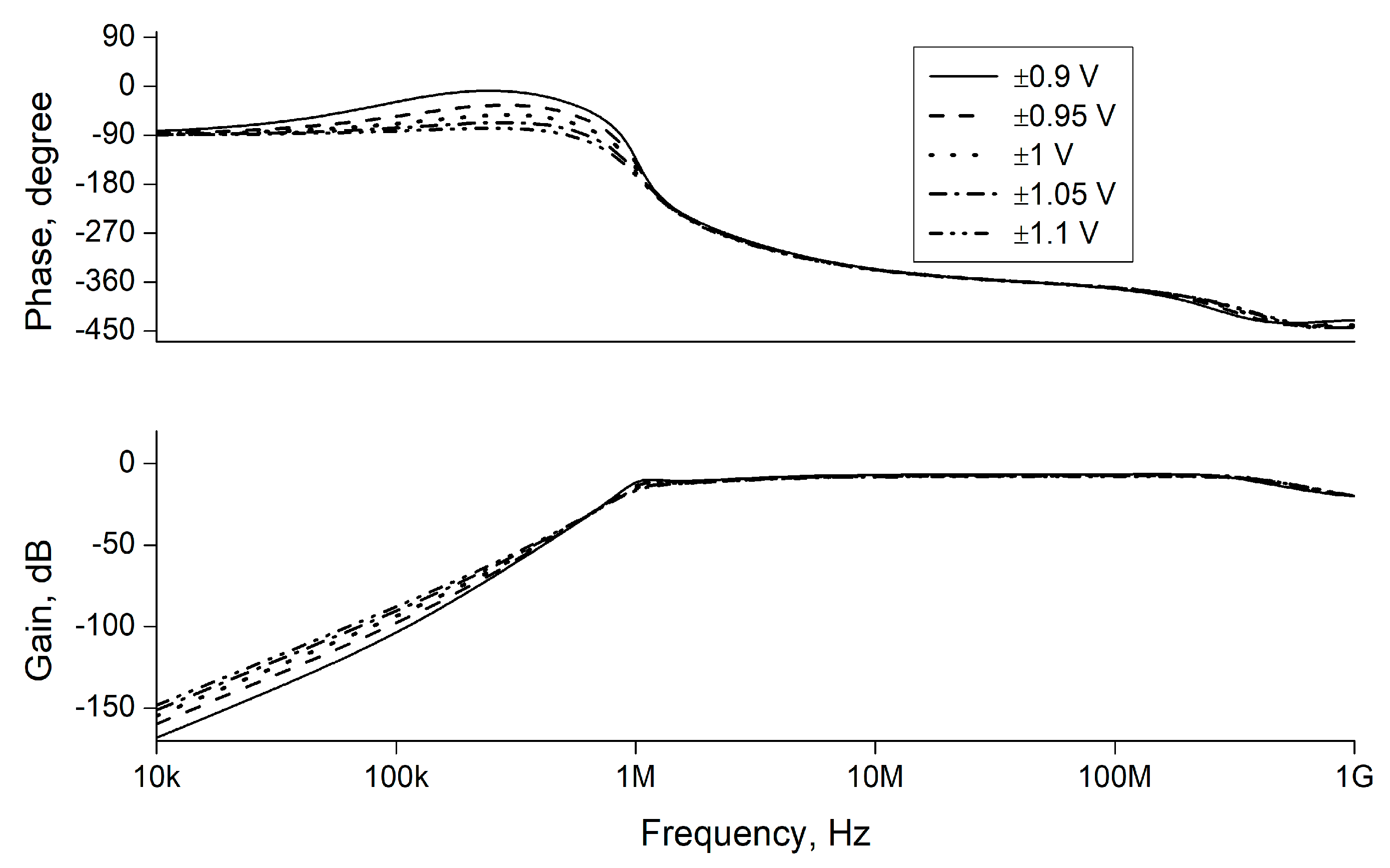
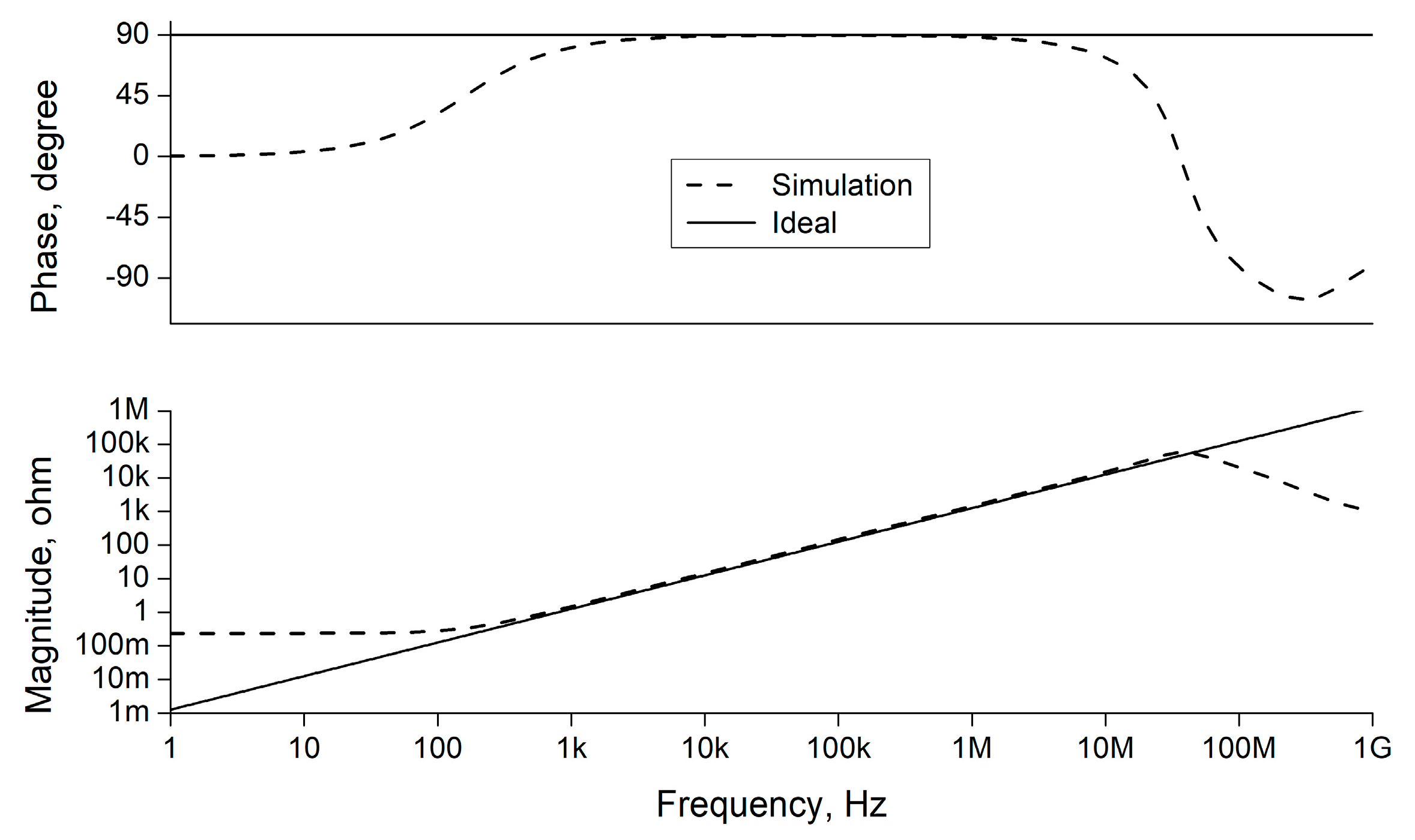
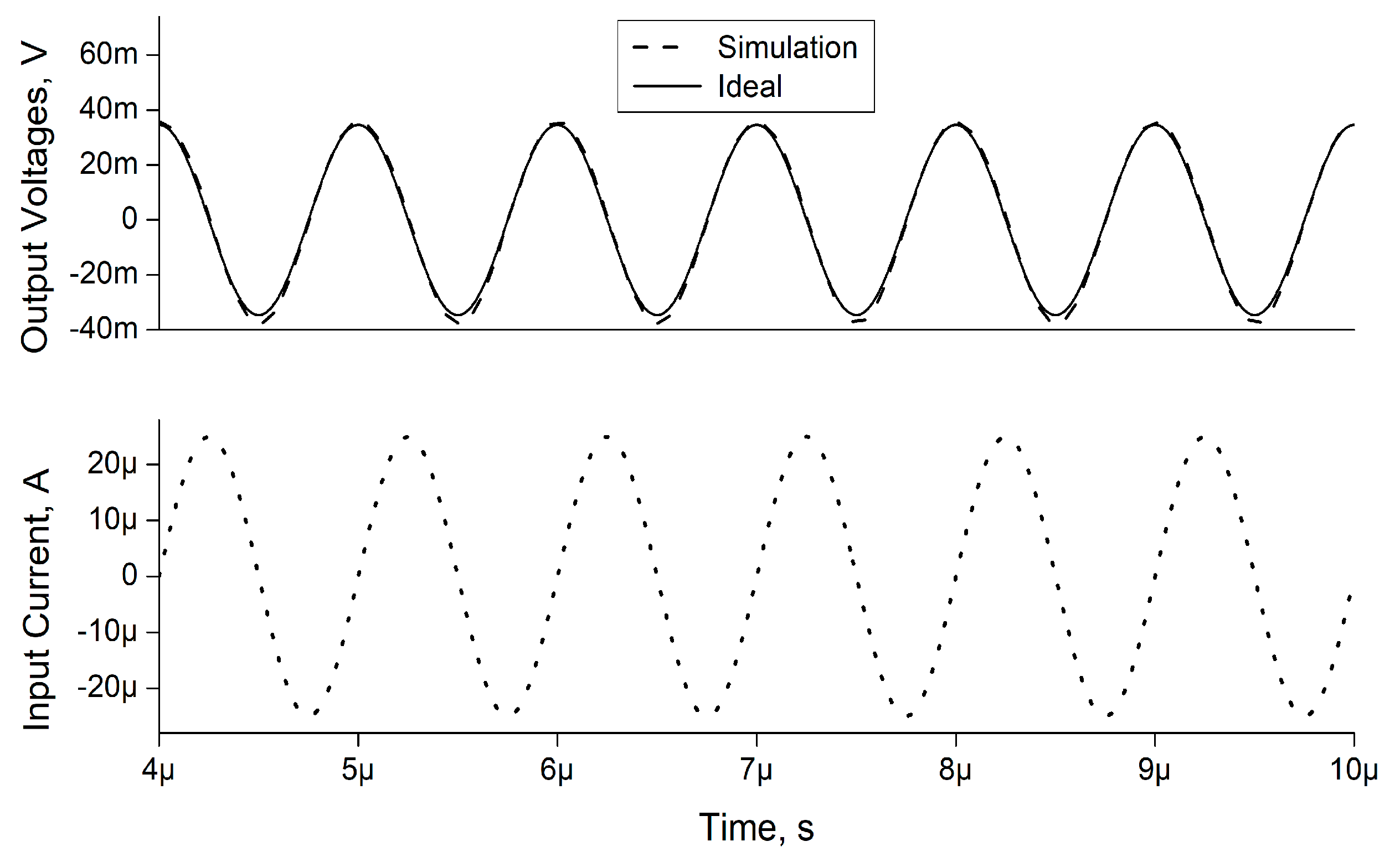
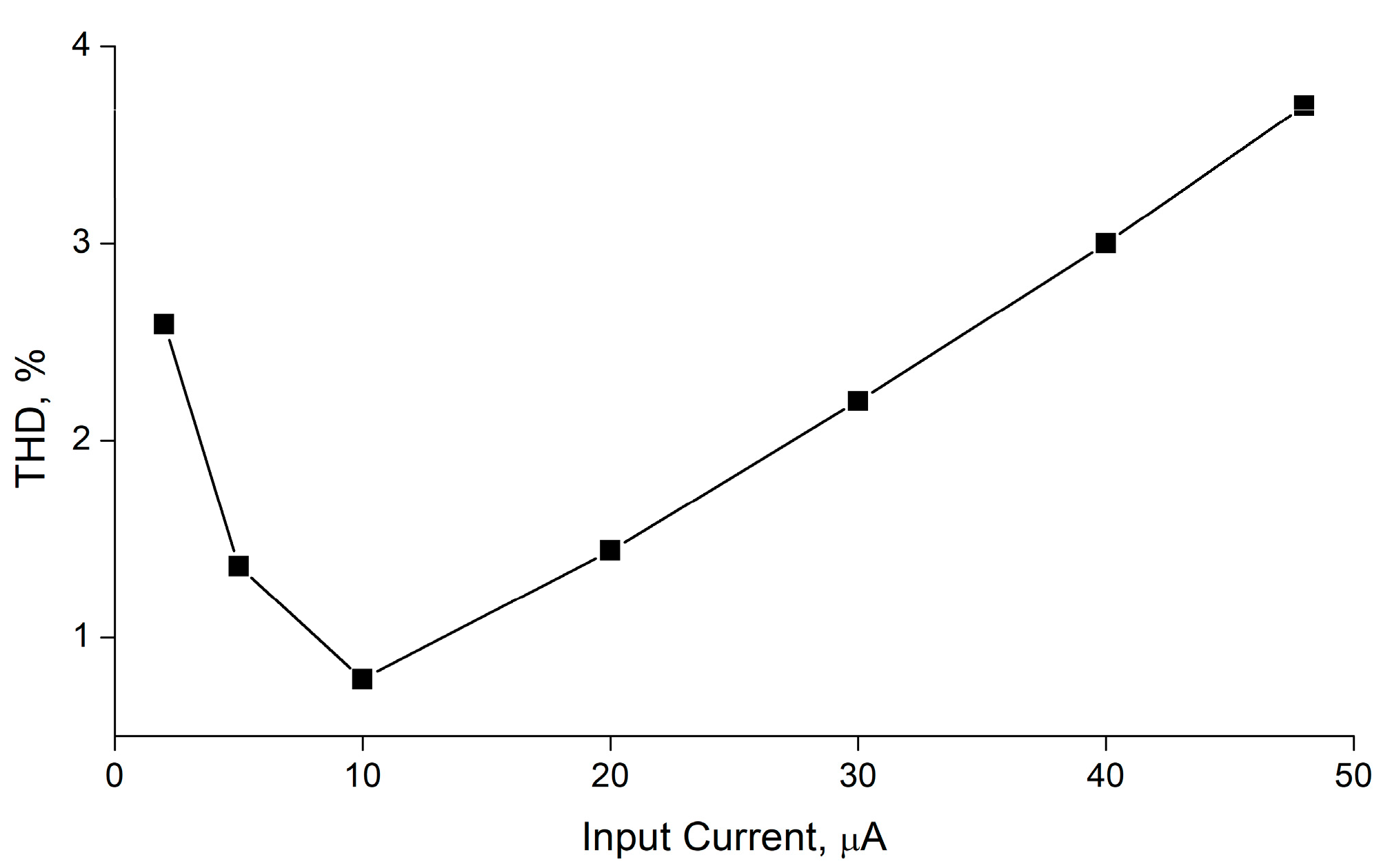
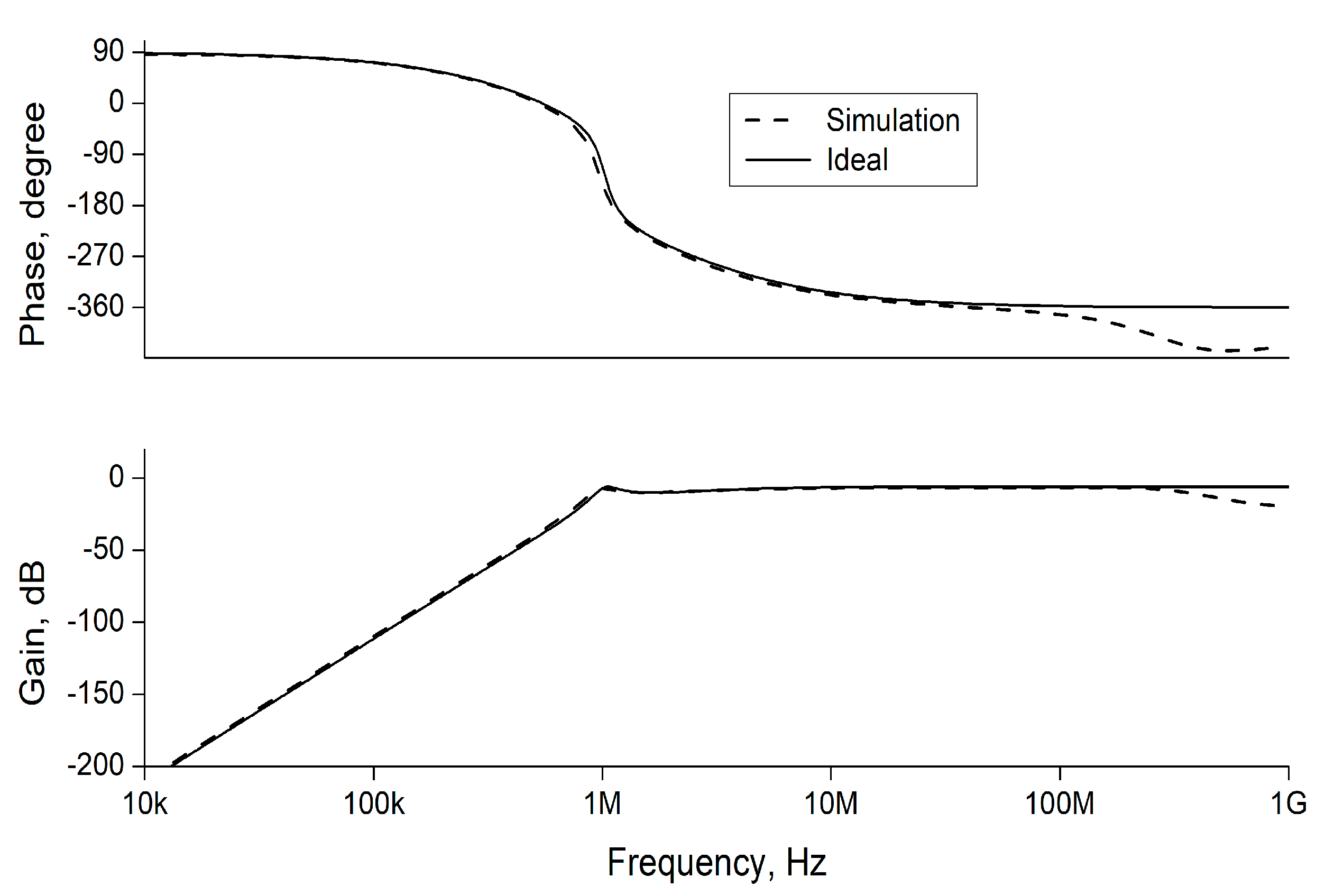
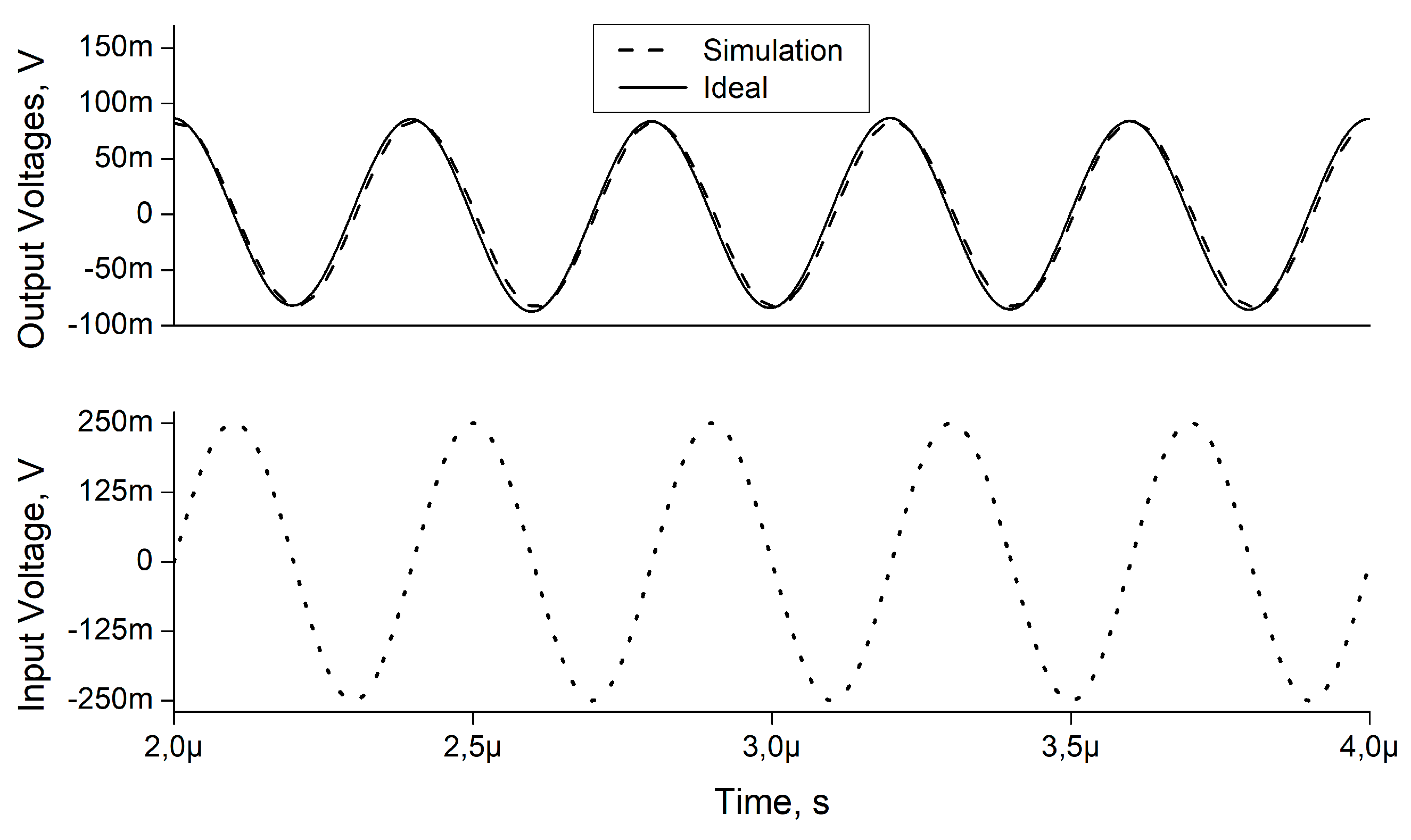
4. Simulation Results

The performance of the proposed circuit of Figure 2 is tested through SPICE simulations using 0.18 μm CMOS technology parameters and a supply voltage of ±0.9 V. The resulted performance parameters for the VCII±, derived from one in Figure 5 [58], are reported in Table 1 in which VB = 0.23 V is chosen. The proposed solution for the implementation of an equivalent inductor is not related to a specific VCII. The size of M13, M9M10 determines the value of rY. The size of M3, M18 determines impedance at X+ port; the size of M8M24 determines the impedance at X− port; and finally the size of M11M12, M14 determines the impedance at Z+ port. Aspect ratios of the PMOS transistors, M1M7 and M9M12, are chosen as 40.5 µm/0.54 µm and M8, M13 and M14 are selected as 81 µm/0.54 µm. Furthermore, those of NMOS transistors, M15–M23, are chosen as 13.5 µm/0.54 µm and that of M24 is selected as 27 µm/0.54 µm. Total power-dissipation of the proposed SI is nearly found as 1.92 mW. To achieve an inductance value of about 200 µH, all the values of passive components are chosen as R1 = 2 kΩ, R2 ≅ 2.16 kΩ and C = 50 pF. Frequency responses of the proposed SI and an ideal inductor are shown in Figure 6. From the simulation results, the operation frequency range of the proposed SI is 1 kHz–10 MHz. The value of series impedance is also obtained as a negligible value of 237 mΩ. To test the time-domain performance of the proposed inductor simulator, a sinusoidal input current with peak amplitude of 25 μA and frequency of 1 MHz is used.
Figure 7 shows the produced output signals along with applied input signal. Additionally, the value of total harmonic distortion (THD) is 1.8%. The value of the phase shift between input current and output voltage is approximately 90°. There is an offset voltage at the simulation output voltage whose value is approximately −12 mV. Figure 8 shows the THD variations for various amplitudes of the peak-input currents at a frequency of 1 MHz. Favorably, the maximum value of THD remains below 3.7%. To test the frequency-domain applicability of the proposed SI, it is used in a standard fifth-order HP ladder filter shown in Figure 9 with Leq1 = Leq2 = 200 µH, RS = RL = 5 kΩ and C1 = C2 = C3 = 50 pF. Frequency-domain analysis for the filer is given in Figure 10. A time-domain analysis for the filter example is depicted in Figure 11, in which a sinusoidal input voltage with a 250 mV peak and a frequency of 2.5 MHz is applied. Figure 12 demonstrates the THD variations for various amplitudes of peak-input voltages at 2.5 MHz. Monte Carlo (MC) simulations are accomplished in 100 runs where all the passive elements of the filter, as shown in Figure 13, are changed by 1%. Furthermore, threshold voltages of all the MOS transistors in Figure 5 are varied by 1% and the result for the filter example is given in Figure 14. Power supplies are varied and the result for the filter example is depicted in Figure 15.
A comparison among the proposed grounded SI with other reported similar works, such as CFOA [4,5,6,7], CCII [8,9,10,11] and VCII-based ones [47,48], is drawn in Table 2, which considers important parameters such as technology, power dissipation, supply voltage, frequency range and the number of grounded and floating passive components, etc. The work reported in [4] suffers from a high supply voltage of ±5V. Although the frequency range of the circuit reported in [7] is limited to 1 kHz, it consumes larger power consumption compared to the proposed circuit because it employs two CFOA as active building blocks. In fact, compared to VCII, which consists of one CB and one VB, the internal structure of each CFOA is formed by one CB and two VBs. Therefore, even in equal conditions, the circuit reported in [7] consumes larger power if compared to the proposed one. The circuit reported in [10], which employs three CCII as active building blocks, is applicable at frequencies larger than 100 kHz while the proposed circuit low-frequency range is 1 kHz. This is attributed to the reduced parasitic series resistance as well as its simplicity, which employs only one active building block; therefore, the number of parasitic elements, which are the frequency-performance limiting factor, is reduced. Although, compared to the previously reported VCII-based SI circuit of [48], the power consumption of the proposed circuit is increased approximately 3 times, but the frequency range is extended from 2.5 MHz to 10 MHz. The work reported in [48] also shows a lossy inductor. In addition, the series resistance is decreased from 191 Ω to 0.23 Ω. Moreover, by setting the values of R1 and R2, the value of a parasitic series resistor can be set as required in the specific application.

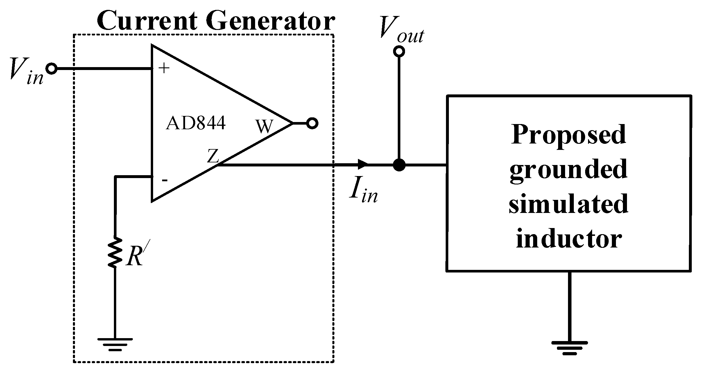
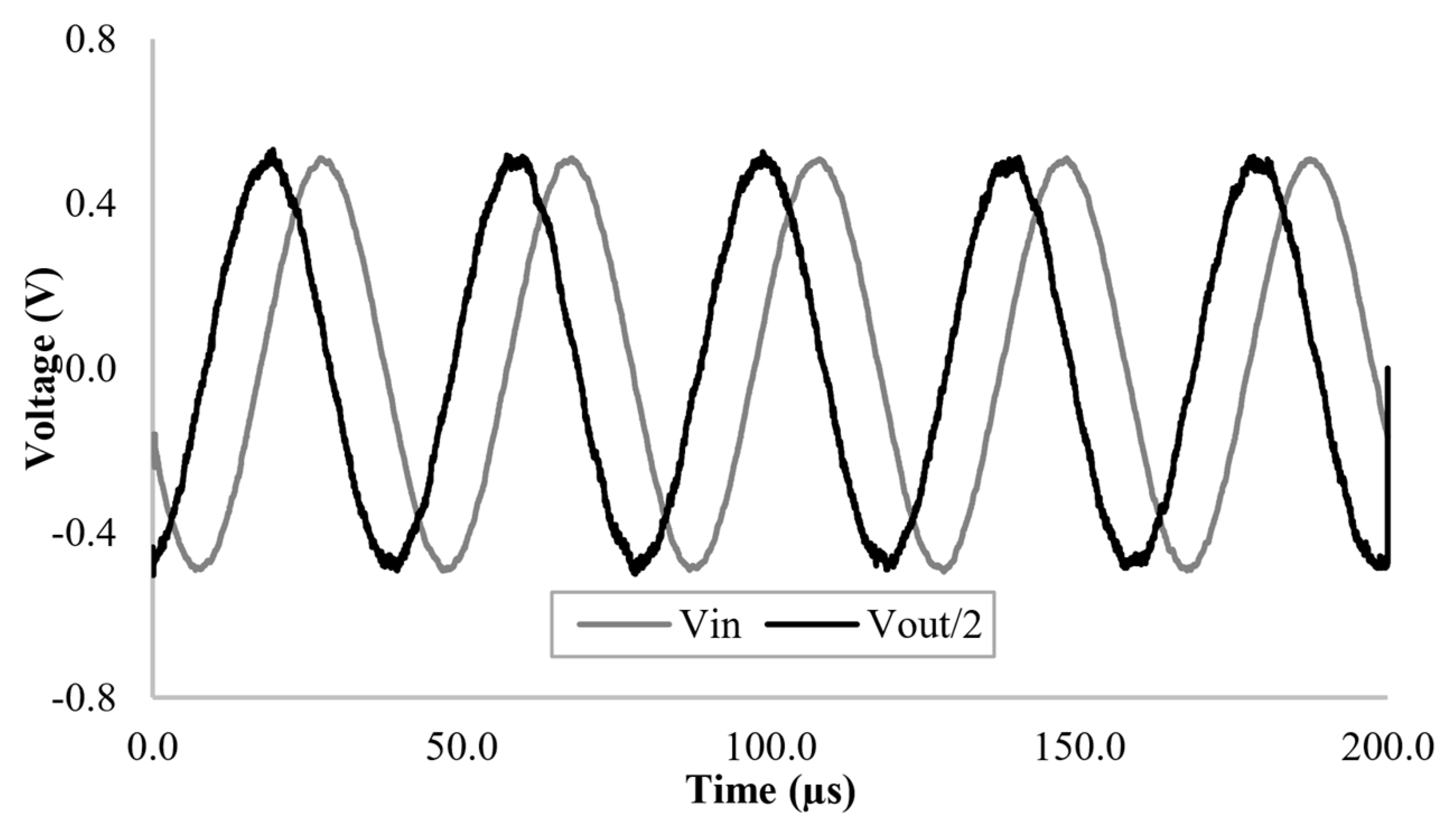
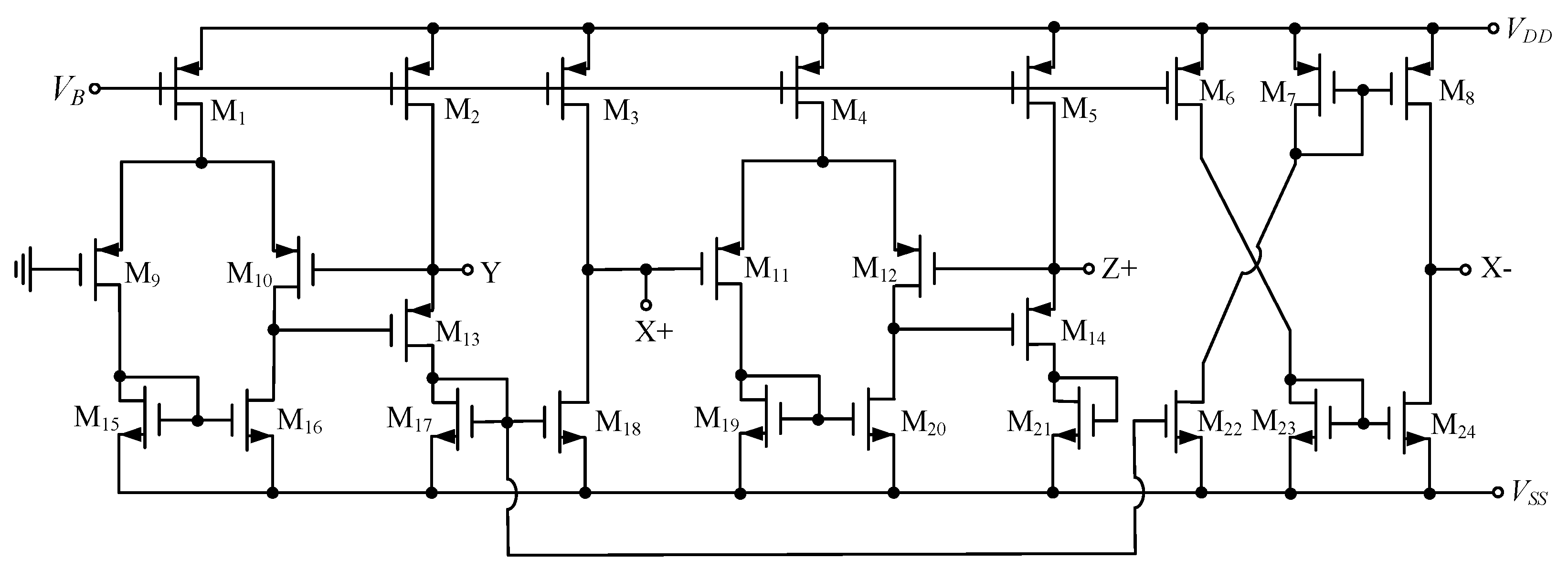
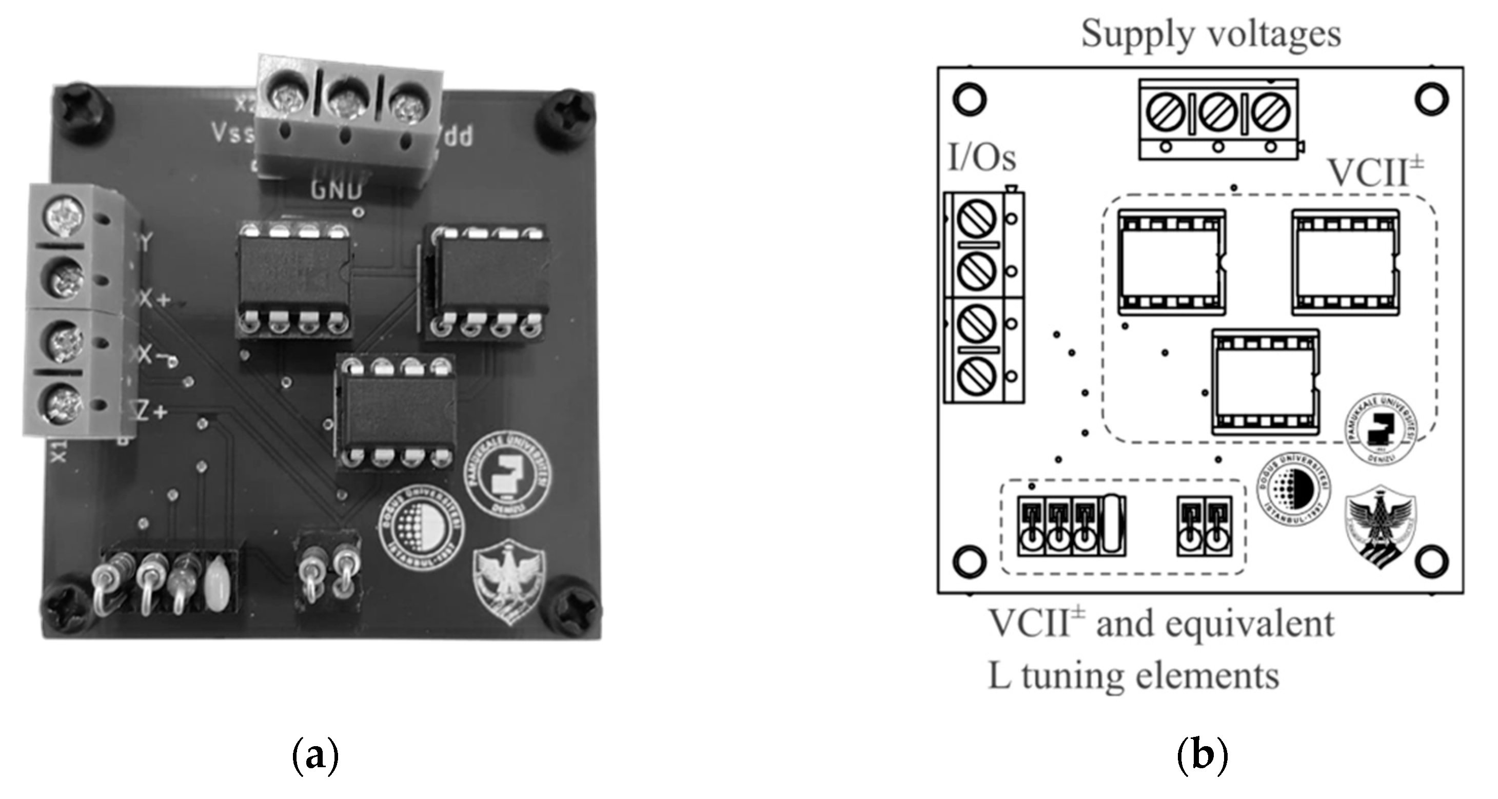
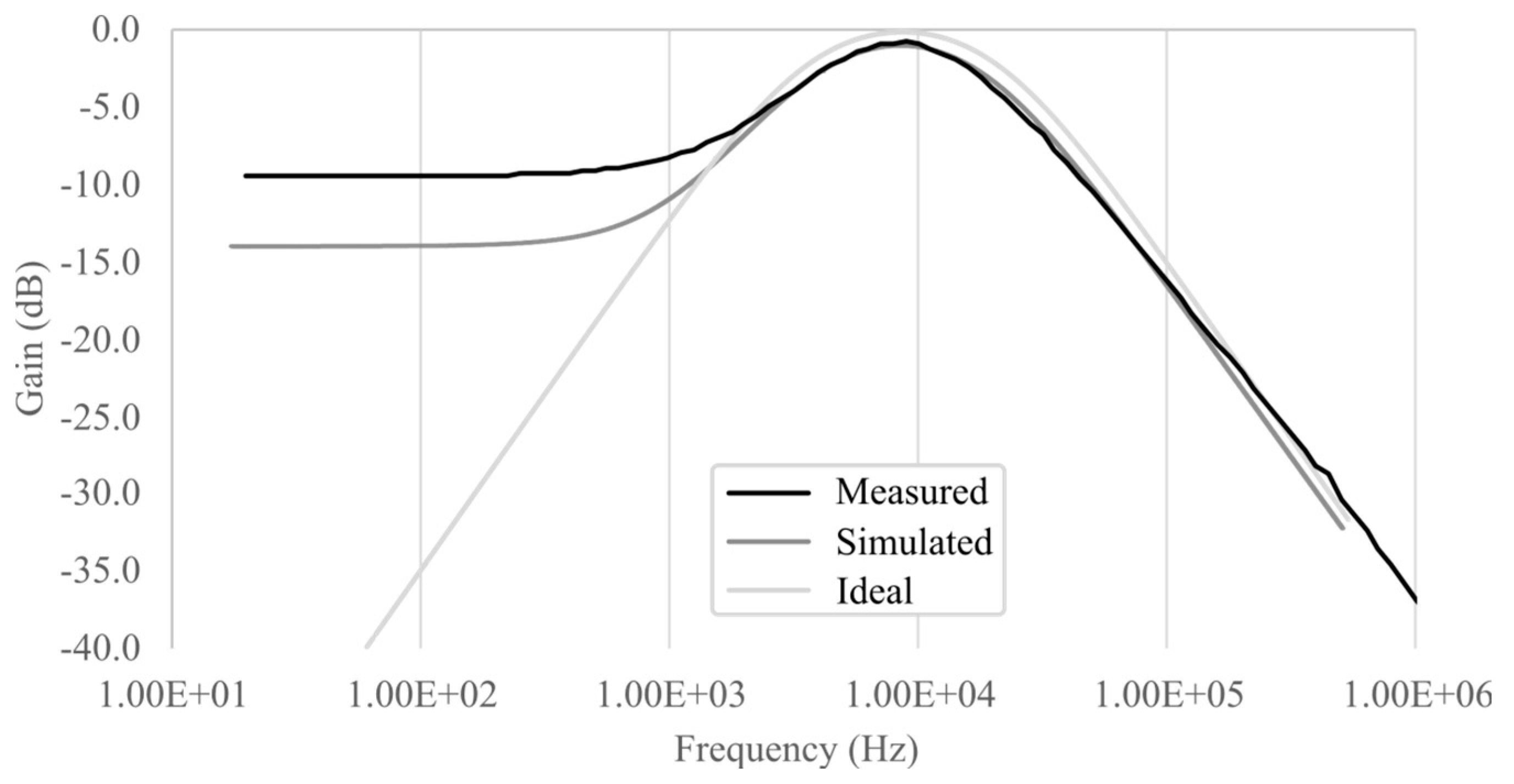
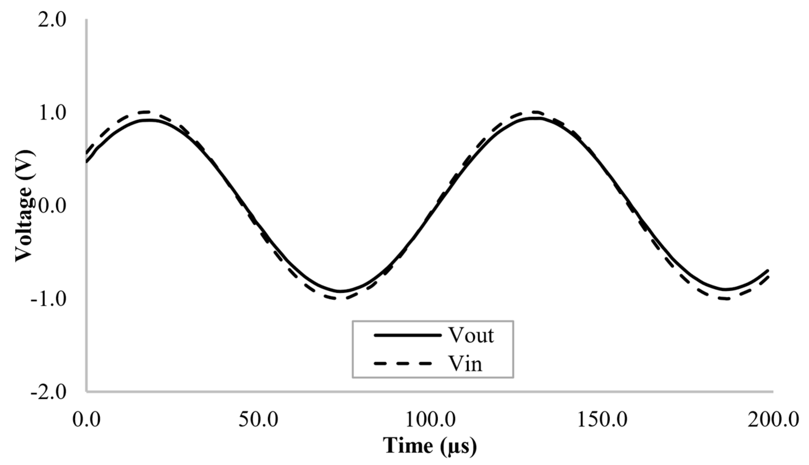
5. Experimental Verifications

Implementation of the VCII± by utilizing AD844s [59] is demonstrated in Figure 16 where supply voltages of AD844s are chosen as ±12 V. Additionally, passive elements Ra = Rb = 2.2 kΩ; Rc = 1.1 kΩ for realizing VCII; R1 = R2 = 2.2 kΩ; and C = 2.2 nF for realizing L, are selected to obtain Leq ≅ 10.65 mH. Figure 17 shows a picture of the fabricated board, highlighting its main features. The experimental setup used to evaluate the equivalent inductance is depicted in Figure 18 where R’ = 1 kΩ is chosen. Thus, a time-domain analysis of the measured grounded SI is given in Figure 19, where a sinusoidal input voltage signal (Vin) with 0.5 V peak at 25 kHz is applied to the input and output voltage taken from Vout. The measured phase shift between them is approximately 86°. A second-order voltage-mode band-pass (BP) filter application is analyzed as well: in Figure 20 the schematic that is used for this experiment is reported. Transfer function of the BP filter in Figure 20 is evaluated as:
H ( s ) = s 1 C f R s 2 + s 1 C f R + 1 L C f
The measured transfer function is reported in Figure 21 and compared to the simulated and the ideal ones. For this analysis the following values are chosen: R ≅ 1 kΩ, R1 ≅ 1.9 kΩ (given in order to improve low-frequency performance); R2 = 2.2 kΩ and C = 2.2 nF, yielding L ≅ 9.2 mH. Additionally, Cf = 30 nF is chosen to obtain f0 ≅ 9.58 kHz. In Figure 21, there is good agreement between ideal, simulated and measurement results above 1kHz. Any discrepancy between these results occurs at frequencies below 1 KHz which is not in the operation frequency range of the proposed circuit and is due to the combined non idealities from AD844s. A time-domain analysis for the BP filter is given in Figure 22 in which a sinusoidal input voltage with 1 V peak-to-peak at f = f0 is applied.
As it is shown in Figure 6, Figure 7 and Figure 8 and Figure 10, Figure 11, Figure 12, Figure 13, Figure 14 and Figure 15 (SPICE simulations) as well as Figure 19, Figure 21 and Figure 22 (experimental verifications), the achieved time- and frequency-domain performances using the proposed SI are very close to ideal ones.

6. Conclusions

A new implementation for the SI based on a single VCII± is proposed. It is composed of one VCII± ABB, two resistors and one grounded capacitor that is attractive for IC fabrication. The prominent feature of the presented work is its low series impedance. As a result, it has the property of improved low-frequency performances. However, it is restricted with a single resistive matching condition. To test the functionality of the proposed circuit, it is used in the realization of a standard fifth-order HP ladder filter and a second-order BP filter. Simulation and experimental results approach to ideal ones but an unimportant difference arises from non-idealities of the VCII±.

Author Contributions

Conceptualization, S.M. and E.Y.; methodology, E.Y. and L.S.; software, E.Y. and L.S.; validation, G.B. and E.Y.; formal analysis, E.Y., L.S. and S.M.; investigation, L.S.; resources, L.S. and G.F.; data curation, G.B. and E.Y.; writing—original draft preparation, E.Y.; writing—review and editing, G.F., S.M. and V.S.; visualization, G.B. and E.Y.; supervision, G.F., V.S. and S.M.; project administration, G.F., V.S. and S.M.; funding acquisition, G.F. and V.S. All authors have read and agreed to the published version of the manuscript.

Funding

This research received no external funding.

Conflicts of Interest

The authors declare no conflict of interest.

References

  1. Antoniou, A. Gyrators using operational amplifiers. Electron. Lett. 1967, 3, 350–352. [Google Scholar] [CrossRef]
  2. Maundy, B.; Gift, S.J.G. Active Grounded Inductor Circuit. Int. J. Electron. 2011, 98, 555–567. [Google Scholar] [CrossRef]
  3. Hamad, A.R.; Ibrahim, M.A. Grounded Generalized Impedance Converter Based on Differential Voltage Current Conveyor (DVCC) and Its Applications. ZANCO J. Pure Appl. Sci. 2017, 29, 118–127. Available online: https://zancojournals.su.edu.krd/index.php/JPAS/article/view/1121 (accessed on 8 June 2021).
  4. Yüce, E.; Minaei, S. On the Realization of Simulated Inductors with Reduced Parasitic Impedance Effects. Circuits Syst. Signal Process. 2009. [Google Scholar] [CrossRef]
  5. Fabre, A. Gyrator Implementation from Commercially Available Transimpedance Operational Amplifiers. Electron. Lett. 1992, 28, 263–264. [Google Scholar] [CrossRef]
  6. Yuce, E. Novel Lossless and Lossy Grounded Inductor Simulators Consisting of a Canonical Number of Components. Analog. Integr. Circuits Signal Process. 2009, 59, 77–82. Available online: https://link.springer.com/article/10.1007/s10470-008-9235-0 (accessed on 1 May 2021).
  7. Yuce, E.; Minaei, S. Commercially Available Active Device Based Grounded Inductor Simulator and Universal Filter with Improved Low Frequency Performances. J. Circuits Syst. Comput. 2017, 26, 1750052. Available online: https://www.worldscientific.com/doi/abs/10.1142/S0218126617500529 (accessed on 1 May 2021).
  8. Sedra, A.; Smith, K. A Second-Generation Current Conveyor and Its Applications. IEEE Trans. Circuit Theory 1970, 17, 132–134. [Google Scholar] [CrossRef]
  9. Çiçekoğlu, O. New Current Conveyor Based Active-Gyrator Implementation. Microelectron. J. 1998, 29, 525–528. [Google Scholar] [CrossRef]
  10. Yuce, E. Grounded Inductor Simulators with Improved Low-Frequency Performances. IEEE Trans. Instrum. Meas. 2008, 57, 1079–1084. [Google Scholar] [CrossRef]
  11. Soliman, A.M. New Active-Gyrator Circuit Using a Single Current Conveyer. Proc. IEEE 1978, 66, 1580–1581. [Google Scholar] [CrossRef]
  12. Alpaslan, H.; Yuce, E. New Grounded Inductor Simulator Using Unity Gain Cells. Indian J. Pure Appl. Phys. 2013, 51, 651–656. [Google Scholar]
  13. Yuce, E.; Alpaslan, H. New CMOS Based Current Follower and Its Applications to Inductor Simulator and Band-Pass Filter. Indian J. Pure Appl. Phys. 2016, 54, 511–516. [Google Scholar]
  14. Alzaher, H. Current Follower Based Reconfigurable Integrator/Differentiator Circuits with Passive and Active Components׳ Reuse. Microelectron. J. 2015, 46, 135–142. [Google Scholar] [CrossRef]
  15. Arslan, E. High Performance Wideband CMOS CCI and Its Application in Inductance Simulator Design. Adv. Electr. Comp. Eng. 2012, 12, 21–26. [Google Scholar] [CrossRef]
  16. Emre Arslan; Ugur Cam; Oguzhan Cicekoglu Novel Lossless Grounded Inductance Simulators Employing Only a Single First Generation Current Conveyor. Frequenz 2003, 57, 204–206. [CrossRef]
  17. Kumar, P.; Senani, R. New Grounded Simulated Inductance Circuit Using a Single PFTFN. Analog Integr. Circuits Signal Process. 2010, 62, 105–112. [Google Scholar] [CrossRef]
  18. Pandey, R.; Pandey, N.; Paul, S.K.; Singh, A.; Sriram, B.; Trivedi, K. Novel Grounded Inductance Simulator Using Single OTRA. Int. J. Circuit Theory Appl. 2014, 42, 1069–1079. Available online: https://onlinelibrary.wiley.com/doi/abs/10.1002/cta.1905 (accessed on 8 June 2021).
  19. Pandey, R.; Pandey, N.; Paul, S.K.; Singh, A.; Sriram, B.; Trivedi, K. New Topologies of Lossless Grounded Inductor Using OTRA. J. Electr. Comput. Eng. 2011. Available online: https://www.hindawi.com/journals/jece/2011/175130/ (accessed on 8 June 2021).
  20. Gülsoy, M.; Cicekoglu, O. Lossless and Lossy Synthetic Inductors Employing Single Current Differencing Buffered Amplifier. IEICE Trans. Commun. 2005. [Google Scholar] [CrossRef]
  21. Toker, A.; Acar, S. CDBA-Based Fully Integrated Gyrator Circuit Suitable for Electronically Tunable Inductance Simulation. AEU Int. J. Electron. Commun. 2000, 54, 293–296. [Google Scholar]
  22. Kaçar, F. New Lossless Inductance Simulators Realization Using a Minimum Active and Passive Components. Microelectron. J. 2010, 41, 109–113. [Google Scholar] [CrossRef]
  23. Kaçar, F.; Yeşil, A.; Minaei, S.; Kuntman, H. Positive/Negative Lossy/Lossless Grounded Inductance Simulators Employing Single VDCC and Only Two Passive Elements. AEU Int. J. Electron. Commun. 2014, 68, 73–78. [Google Scholar] [CrossRef]
  24. Metin, B. Supplementary Inductance Simulator Topologies Employing Single DXCCII; Brno University of Technology: Brno, Czech Republic, 2011. [Google Scholar]
  25. Kaçar, F.; Yeşil, A. Novel Grounded Parallel Inductance Simulators Realization Using a Minimum Number of Active and Passive Components. Microelectron. J. 2010, 41, 632–638. [Google Scholar] [CrossRef]
  26. Yeşil, A.; Kaçar, F. New DXCCII-Based Grounded Series Inductance Simulator Topologies; Istanbul University: İstanbul, Turkey, 2014. [Google Scholar]
  27. Myderrizi, I.; Minaei, S.; Yuce, E. DXCCII-Based Grounded Inductance Simulators and Filter Applications. Microelectron. J. 2011, 42, 1074–1081. [Google Scholar] [CrossRef]
  28. Metin, B.; Herencsar, N.; Koton, J.; Horng, J.-W. DCCII-Based Novel Lossless Grounded Inductance Simulators with No Element Matching Constrains. Radioengineering 2014, 23, 532–539. [Google Scholar]
  29. Metin, B. Canonical Inductor Simulators with Grounded Capacitors Using DCCII. Int. J. Electron. 2012, 99, 1027–1035. Available online: https://www.tandfonline.com/doi/abs/10.1080/00207217.2011.639274 (accessed on 8 June 2021).
  30. Herencsar, N.; Lahiri, A.; Koton, J.; Vrba, K.; Metin, B. Realization of Resistorless Lossless Positive and Negative Grounded Inductor Simulators Using Single ZC-CCCITA; Radioengineering, Czech Technical University: Praha, Czech Republic, 2012. [Google Scholar]
  31. Bhaskar, D.R.; Prasad, D.; Singh, A.K. New Grounded and Floating Simulated Inductance Circuits Using Current Differencing Transconductance Amplifiers; Radioengineering, Czech Technical University: Praha, Czech Republic, 2010. [Google Scholar]
  32. Srivastava, M.; Prasad, D.; Bhaskar, D. New Electronically Tunable Grounded Inductor Simulator Employing Single VDTA and One Grounded Capacitor. J. Eng. Sci. Technol. 2017, 12, 113–126. [Google Scholar]
  33. Herencsar, N.; Koton, J.; Vrbra, K. CFTA-Based Active-C Grounded Positive Inductance Simulator and Its Application. Elektrorevue 2010, 1, 24–27. Available online: http://elektrorevue.cz/en/articles/analogue-technics/0/cfta-based-active-c-grounded-positive-inductance-simulator-and-its-application-1/ (accessed on 8 June 2021).
  34. Psychalinos, C.; Spanidou, A. Current Amplifier Based Grounded and Floating Inductance Simulators. AEU Int. J. Electron. Commun. 2006, 60, 168–171. [Google Scholar] [CrossRef]
  35. Yeşil, A.; Kaçar, F.; Gürkan, K. Lossless Grounded Inductance Simulator Employing Single VDBA and Its Experimental Band-Pass Filter Application. AEU Int. J. Electron. Commun. 2014, 68, 143–150. [Google Scholar] [CrossRef]
  36. Singh, A.; Kumar, P.; Senani, R. Electronically Tunable Grounded/Oating Inductance Simulators Using Z-Copy CFCCC. Turk. J. Electr. Eng. Comput. Sci. 2018, 26, 1041–1055. [Google Scholar] [CrossRef]
  37. Siripongdee, S.; Jaikla, W. Electronically Controllable Grounded Inductance Simulators Using Single Commercially Available IC: LT1228. AEU—Int. J. Electron. Commun. 2017, 76, 1–10. [Google Scholar] [CrossRef]
  38. Agrawal, D.; Maheshwari, S. Electronically Tunable Grounded Immittance Simulators Using an EX-CCCII. Int. J. Electron. 2020, 107, 1625–1648. Available online: https://www.tandfonline.com/doi/abs/10.1080/00207217.2020.1729421 (accessed on 8 June 2021).
  39. Yesil, A.; Yuce, E.; Minaei, S. Inverting Voltage Buffer Based Lossless Grounded Inductor Simulators. AEU Int. J. Electron. Commun. 2018, 83, 131–137. [Google Scholar] [CrossRef]
  40. Abaci, A.; Yuce, E. Modified DVCC Based Quadrature Oscillator and Lossless Grounded Inductor Simulator Using Grounded Capacitor(s). AEU Int. J. Electron. Commun. 2017, 76, 86–96. [Google Scholar] [CrossRef]
  41. Koton, J.; Yuce, E.; Ibrahim, M.A.; Herencsar, N.; Minaei, S. Lossy/Lossless Floating/Grounded Inductance Simulation Using One DDCC; Radioengineering, Czech Technical University: Praha, Czech Republic, 2012. [Google Scholar]
  42. Yuce, E.; Minaei, S. A Modified CFOA and Its Applications to Simulated Inductors, Capacitance Multipliers, and Analog Filters. IEEE Trans. Circuits Syst. I Regul. Pap. 2008, 55, 266–275. [Google Scholar] [CrossRef]
  43. Alpaslan, H.; Yuce, E. Inverting CFOA Based Lossless and Lossy Grounded Inductor Simulators. Circuits Syst. Signal Process. 2015, 34, 3081–3100. Available online: https://link.springer.com/article/10.1007/s00034-015-0004-x (accessed on 8 June 2021).
  44. Yuce, E.; Minaei, S.; Cicekoglu, O. A Novel Grounded Inductor Realization Using a Minimum Number of Active and Passive Components. ETRI J 2005, 27, 427–432. [Google Scholar] [CrossRef]
  45. Yuce, E.; Minaei, S.; Cicekoglu, O. Limitations of the Simulated Inductors Based on a Single Current Conveyor. IEEE Trans. Circuits Syst. I: Regul. Pap. 2006, 53, 2860–2867. [Google Scholar] [CrossRef]
  46. Yuce, E. Inductor Implementation Using a Canonical Number of Active and Passive Elements. Int. J. Electron. 2007, 94, 317–326. Available online: https://www.tandfonline.com/doi/abs/10.1080/00207210701257343 (accessed on 8 June 2021).
  47. Filanovsky, I.M. Current Conveyor, Voltage Conveyor, Gyrator. In Proceedings of the 44th IEEE 2001 Midwest Symposium on Circuits and Systems. MWSCAS 2001 (Cat. No.01CH37257), Dayton, OH, USA, 14–17 August 2001; Volume 1, pp. 314–317. [Google Scholar]
  48. Safari, L.; Yuce, E.; Minaei, S.; Ferri, G.; Stornelli, V. A Second-generation Voltage Conveyor (VCII)–Based Simulated Grounded Inductor. Int. J. Circuit Theory Appl. 2020, 48, 1180–1193. Available online: https://onlinelibrary.wiley.com/doi/abs/10.1002/cta.2770 (accessed on 8 June 2021).
  49. Yuce, E.; Alpaslan, H.; Minaei, S.; Ayten, U.E. A new simulated grounded inductor based on two NICs, two resistors and a grounded capacitor. Circuits Syst. Signal Process. 2021. [Google Scholar] [CrossRef]
  50. Yuce, E.; Minaei, S. Universal Current-Mode Filters and Parasitic Impedance Effects on the Filter Performances. Int. J. Circuit Theory Appl. 2008, 36, 161–171. [Google Scholar] [CrossRef]
  51. Fabre, A.; Saaid, O.; Wiest, F.; Boucheron, C. High Frequency Applications Based on a New Current Controlled Conveyor. IEEE Trans. Circuits Syst. I: Fundam. Theory Appl. 1996, 43, 82–91. [Google Scholar] [CrossRef]
  52. Ferri, G.; Guerrini, N.C. Low-Voltage Low-Power CMOS Current Conveyors; Springer: Berlin/Heidelberg, Germany, 2003; ISBN 978-1-4020-7486-8. [Google Scholar]
  53. Toumazou, C.; Lidgey, F.J.; Haigh, D. Analogue IC Design: The Current-Mode Approach; IET: Stevenage, UK, 1993; ISBN 978-0-86341-297-4. [Google Scholar]
  54. Filanovsky, I.M.; Stromsmoe, K.A. Current-Voltage Conveyor. Electron. Lett. 1981, 17, 129–130. [Google Scholar] [CrossRef]
  55. Yesil, A.; Minaei, S. New Simple Transistor Realizations of Second-Generation Voltage Conveyor. Int. J. Circuit Theory Appl. 2020, 48, 2023–2038. [Google Scholar] [CrossRef]
  56. Safari, L.; Barile, G.; Stornelli, V.; Ferri, G. An Overview on the Second Generation Voltage Conveyor: Features, Design and Applications. IEEE Trans. Circuits Syst. II Express Briefs 2019, 66, 547–551. [Google Scholar] [CrossRef]
  57. Stornelli, V.; Safari, L.; Barile, G.; Ferri, G. A New Extremely Low Power Temperature Insensitive Electronically Tunable VCII-Based Grounded Capacitance Multiplier. IEEE Trans. Circuits Syst. II Express Briefs 2021, 68, 72–76. [Google Scholar] [CrossRef]
  58. Surakampontorn, W.; Riewruja, V.; Kumwachara, K.; Dejhan, K. Accurate CMOS-Based Current Conveyors. IEEE Trans. Instrum. Meas. 1991, 40, 699–702. [Google Scholar] [CrossRef]
  59. AD844 60 MHz Monolithic Op amp. Available online: https://www.analog.com/media/en/technical-documentation/data-sheets/AD844.pdf (accessed on 1 May 2021).
Figure 1. VCII± without Z− port: (a) symbolic presentation (b) internal structure.
Electronics 10 01693 g001
Figure 2. Proposed VCII±-based simulated inductor.
Electronics 10 01693 g002
Figure 3. VCII± and its parasitic impedances.
Electronics 10 01693 g003
Figure 4. Equivalent model of the proposed simulated inductor.
Electronics 10 01693 g004
Figure 5. Internal structure of the used VCII± without Z− terminal.
Electronics 10 01693 g005
Figure 6. Frequency responses of the proposed simulated inductor and ideal inductor.
Electronics 10 01693 g006
Figure 7. Time-domain responses of the proposed simulated inductor.
Electronics 10 01693 g007
Figure 8. THD values of output voltages of the proposed simulated inductor for different peak values of the input currents.
Electronics 10 01693 g008
Figure 9. Standard fifth-order high-pass ladder filter realization [49].
Electronics 10 01693 g009
Figure 10. Frequency responses of the fifth-order high-pass ladder filter example.
Electronics 10 01693 g010
Figure 11. Time-domain analysis for the HP ladder filter example.
Electronics 10 01693 g011
Figure 12. THD variations of the HP ladder filter for various amplitudes of the peak-input voltages at 2.5 MHz.
Electronics 10 01693 g012
Figure 13. Monte Carlo simulations of the HP ladder filter with changes of all the passive elements.
Electronics 10 01693 g013
Figure 14. Monte Carlo simulations of the HP ladder filter with changes of threshold voltages of all the MOS transistors.
Electronics 10 01693 g014
Figure 15. Frequency responses of the HP ladder filter for different power supplies.
Electronics 10 01693 g015
Figure 16. Implementation of the VCII± by utilizing AD844s.
Electronics 10 01693 g016
Figure 17. A photograph of the fabricated board (a) and its description (b).
Electronics 10 01693 g017
Figure 18. Experimental setup for realizing the grounded simulated inductor.
Electronics 10 01693 g018
Figure 19. Measured time-domain analysis of the grounded simulated inductor.
Electronics 10 01693 g019
Figure 20. A second-order voltage-mode band-pass filter application.
Electronics 10 01693 g020
Figure 21. Experimental, simulation and ideal gain responses versus frequency.
Electronics 10 01693 g021
Figure 22. A time-domain analysis for the band-pass filter.
Electronics 10 01693 g022
Table 1. Some performance parameters of the VCII± of Figure 5.
ParameterValueParameterValue
RY19 Ωβ1.004
RX+41 kΩη2.021
RX−20 kΩα0.973
RZ+19 Ω
CX+143 fF
CX−111 fF
Table 2. A comparison among the proposed circuit and some other previously reported similar works.
Reference# ABB (Type)# of Passive ElementsFrequency RangeTechnologyPower Dissipation (mW)VDD-VSSImproved Low Frequency Performance
# of R
G (F)
# of C
G (F)
[4]3 (CFOA)2 (1)1 (0)1 μHz–1 MHzAD844NA±5Yes
[5]2 (CFOA)1 (1)1 (0)NAAD844NANANo
[6] *1 (CFOA)1 (1)0 (1)LowAD844NA±15No
[7]2 (CFOA)2 (1)1 (0)1 kHz–100 MHz0.13 μm3.05±0.75Yes
[8]2 (CCII)2 (0)1 (0)NANANANANo
[9]2 (CCII)2 (0)1 (0)NAAD844NA±12No
[10]3 (CCII)2 (1)1 (0)100 kHz–100 MHz0.35 μmNA±1.5Yes
[11]1 (CCII)2 (2)0 (1)NANANANANo
[47] *MOS transistors2 (0)0 (1)<1 kHzNANANANo
[48]2 (VCII)0 (2)1 (0)50 kHz–2.5 MHz0.18 μm0.65±0.9VNo
Proposed1 VCII±0 (2)1 (0)1 kHz–10 MHz0.18 μm1.92±0.9VYes
G: grounded, F: floating, NA: not available, *: lossy.
Publisher’s Note: MDPI stays neutral with regard to jurisdictional claims in published maps and institutional affiliations.

