Abstract
This paper aims at solving one challenging problem in designing VLSI chips, namely, the security of the hardware, by presenting a new design approach that incorporates the obfuscation technique in the VLSI implementation of some important DSP algorithms. The proposed method introduces a new approach in obtaining a unified VLSI architecture for computing type IV discrete cosine transform (DCT-IV) and type IV discrete sine transform (DST-IV), with an efficient integration of the obfuscation technique, while maintaining low overheads. The algorithms for these two transforms were restructured in such a way that their structures are fairly similar, and thus they can be implemented on the same VLSI chip and on the same hardware with very few modifications, with the latter being attributed to the pre-processing and post-processing stages. The design proposed uses the regular and modular structures, which are named quasi-correlation, and the architecture is inspired by the paradigm of the systolic array architecture. Thus, the introduced design benefits the security, for the hardware, and also the advantages introduced by the use of the regular and modular structures. A very efficient, unified VLSI architecture for type IV DCT/DST can be obtained, which allows the computation of the two algorithms on the same hardware, allowing an efficient incorporation of the obfuscation technique with very low overheads, and it can be very efficiently implemented, offering high-speed performances and low hardware complexity, with the latter being attributed to the efficient use of the hardware resources for the computation of these two algorithms.
1. Introduction
In the past years, we have seen the telemedicine field growing and being one of great interest, and, in the current environment, where the online world is starting to take precedence, this field is also starting to become a vital one. The term telemedicine in itself could be simply translated to remote medicine, and an aspect of utmost importance for achieving the remote condition is data transmission and, of course, beforehand, data compression.
The discrete transforms DCT-IV and DST-IV, which were first introduced by Jain [1], have spectral analysis, signal processing and image coding as their main applications [2,3,4,5], and as such are valid candidates for being used in the telemedicine field. However, these two transforms are computationally intensive and, as such, they need to be restructured to ensure they are fit for being used in applications in real-time.
For a VLSI implementation and, moreover, an efficient one, one needs to take into account the data flow within the algorithm’s structure, thus the relationship with both its complexity and architecture. In this sense, the present paper proposes reformulated algorithms for the calculation of both DCT-IV and DST-IV, in a such manner that an efficient unified VLSI architecture can be obtained, based on structures that are regular and modular, such as cyclic convolution and circular correlation, and that can be used for an efficient VLSI implementation through the paradigm of systolic arrays architecture [5,6].
1.1. Data Security
Data security is a complex phenomenon today, and is one of the most challenging issues of the 21st century. Computer security in the era of the Internet of Things (IoTs) and Cloud Storage and Computing is more and more important. At the software level, access control is one of the most important aspects of computer security. In [7], there are several solutions for access control presented, both traditional and modern ones, such as the following: discretionary access control, mandatory access control, role-based access control, attribute-based access control, etc., and context information in pervasive computing domain, the RBAC approaches with spatial and temporal contexts, the RBAC approaches with user, resource and environment-centric contexts, the RBAC approaches with relationship contexts, the RBAC approaches with situational contexts, etc., for context aware access control. As we can see, there were a lot of works on this subject that show its importance. Some of the ideas that were developed for software security techniques can also be used to develop hardware security measures. In the following, we will limit only to the hardware security solutions and, more specifically, to obfuscation techniques.
Nowadays, when it is necessary to integrate different IP macro-cells using global supply vendors, it is more and more important [8] to protect the design from piracy, malicious alteration, or reverse engineering, resulting in Trojan threats [9].
The value of the modern products is mainly given by the new valuable ideas that are incorporated into them. In the world of VLSI circuits, the research and development costs are indeed extremely high, and the protection of their intellectual property rights is of great importance. By overbuilding, an another company can sell ICs that are obtained by piracy, and counterfeit and sell them illegally at a lower cost. Also, by reverse engineering of the design, an untrusted company can extract a gate-level netlist of the chip, to steal valuable information that can be incorporated in its own chips.
Thus, the problem of hardware security is one of great importance, which has led to a lot of research that can be mainly classified as follows:
- (1)
- Authentication-based approach;
- (2)
- Obfuscation-based approach.
In this article, we will concentrate on obfuscation-based techniques, which is one of the most important solutions for this problem [10,11,12,13,14,15,16].
For a logic encryption, which uses key gates, the latter are used for the purpose of obfuscation. This way, for each key that is used, the true signal is transmitted, and, for erroneous keys, an obfuscated false output signal will be the result.
One of the main techniques to obtain obfuscation is mode-based obfuscation [16,17]. This technique is used to design obfuscated functions by creating correct and incorrect functional modes. The system will work in the desired mode if a correct key is used to select this mode. The most simple mean to obtain this is by modifying the control flow in the design and not the data path, by altering the control signals to obtain incorrect modes.
Koteshwara introduced, in the paper “Key-Based Dynamic Functional Obfuscation of Integrated Circuits using Sequentially-Triggered Mode-Based Design” in 2017, the following three types of obfuscation: fixed obfuscation, time-varying obfuscation, and dynamic obfuscation [9].
We are addressing one challenging problem, which is the obfuscation of DSP circuits. In [18], an obfuscating technique based on high-level transformations was proposed. This approach also alters the data path, in order to obtain meaningful modes other than the correct one. We are using an obfuscating method based on high-level transformations and altering the obtained control flow.
1.2. Presentation of the State-of-the-Art
There are many efficient VLSI implementations for direct and inverse DCT [19,20,21,22,23,24], but few optimal VLSI implementations for type IV DCT or type IV DST [5,12,15,25,26,27,28], and even fewer unified solutions to integrate both types of the two transforms on the same chip [11,13,28].
In [5], a VLSI algorithm for DCT-IV based on cyclic convolution structures that can be efficiently implemented in VLSI is proposed, but it cannot be efficiently unified with DST-IV, and it cannot be used to efficiently embed the obfuscation technique, due to the absence of appropriate control bits.
In [25], a hardware accelerator for DCT-IV based on a recursive algorithm is presented. The obtained architecture is even more difficult to use to obtain an obfuscated VLSI chip for DCT-IV.
In [29], the authors introduce a unified VLSI architecture for DCT/DST-IV that uses a VLSI algorithm based on cycle convolutions, as in [5], but the throughput in this case is half of that obtained in [5], and it also cannot be used to efficiently include the obfuscation technique.
There are also recently proposed efficient algorithms for DCT-IV or DST-IV, as in [18,30]; however, they are mainly dedicated to software implementations.
In [17], a fast algorithm for DCT-IV based on recursive decomposition of the DCT-IV matrix is presented, and in [30] we see a fast algorithm for DST-IV presented, based on SFG graph representation and manipulations.
Thus, we have to derive new VLSI algorithms that can be used to obtain a high-performance unified VLSI architecture for DCT/DST-IV, and that allow an efficient incorporation of the obfuscation technique.
Until now, there has been no efficient VLSI implementation for type IV DCT or DST, except for our paper that was presented at TSP 2020 [26], which allows efficient implementation of a hardware security technique.
As was shown in [26], it is possible to reformulate DCT-IV based on pseudo-correlation structures, with the added advantage of securing hardware security by implementing the time-varying obfuscation technique. It is possible to have a unified algorithm for computing more than one transform. Based on the obfuscation technique introduced in [9], and developed in the method presented in [26], this paper introduces a unified architecture, with the same added advantage of hardware security, for both DCT-IV and DST-IV; this way it offers the possibility of selecting and using the transform that is most suited for the respective needed application, and, due to the similarity of the structures, they can both be implemented on the same VLSI chip. Thus, in our paper presented at TSP 2020 [26], we proposed a new approach to efficiently incorporate the obfuscation technique in the VLSI implementation of type IV DCT, which allows high-speed performances to be obtained, using parallel processing and pipelining with low hardware complexity. To our best knowledge, this is the first of such a solution. In the present paper, we extend the approach presented in [26] to obtain a very efficient unified VLSI architecture for type IV DCT/DST, with very low overheads necessary to unify the two architectures, based on a new VLSI algorithm for type IV DST that can be computed on almost the same hardware as type IV DST. To our best knowledge, this is a completely new approach for obtaining a unified type IV DCT/DST that efficiently incorporates a hardware security technique.
1.3. The Main Contributions of the Paper
The problem of hardware security is one of the major challenges of the 21st century, with high economic implications. Efficient embedding of obfuscation-based IP protection, without affecting the high performances required and with low overheads, is a difficult approach, and a few efficient solutions are presented in the literature. In this paper, we intend to propose a new approach for obtaining a high-performance unified VLSI architecture for such a DSP algorithm, which allows efficient imbedding of the obfuscation technique.
The main contributions are:
- A new unified approach to obtain a unified VLSI architecture that allows efficient implementation of an obfuscation technique and improves, at the same time, the high performances of VLSI implementation;
- A new unified VLSI algorithm for DCT/DST-IV that allows efficient unification of the two transforms, and allows efficient implementation of the obfuscation technique;
- A new unified VLSI architecture for DCT/DST-IV that has embedded the new obfuscation technique;
- A new obfuscation technique that circulates a sequence of security keys that renders the detection of the correct keys significantly more difficult, because the keys are changing dynamically and not only the correct keys have to be determined, but also the correct sequence;
- The new obfuscation technique allows a low area, low power and zero performances overhead in the embedding, while maintaining the high performances of the VLSI implementation of type IV DCT/DST.
The rest of the paper is organized as follows: in Section 2, we present the VLSI algorithm for type IV DCT and we propose a new VLSI algorithm for type IV DST, which can be efficiently unified with the first one. Also, we present the VLSI architecture that implements the VLSI algorithms presented before. In Section 3, we present the obtained unified VLSI architecture for type IV DCT/DST, which can execute the two VLSI algorithms on the same hardware with very few changes, and efficiently incorporate the obfuscation technique. In Section 4, we discuss the results, and in Section 5, we draw the conclusions.
2. Methods
Table 1 contains the explanations for the notations used in this paper that will be referenced throughout Section 2.1, Section 2.2, Section 2.3 and Section 2.4.

Table 1.
Notations.
2.1. VLSI Algorithm for DCT-IV
We are firstly describing the algorithm introduced in [26]. Thus, for a real input sequence x(i), type IV DCT (DCT-IV) is defined as follows:
where k = 0, 1, …, N − 1,
and where the following applies:
Next, we remove the constant coefficient from the DCT-IV equation and add a multiplier for scaling the output, using this constant after the VLSI array.
With the goal of achieving an efficient VLSI algorithm, we need to reformulate Equation (1) and, for doing this, we use a new input chain for restructuring.
The output sequence x(k) can be calculated using the equation below:
where k = 1, …, N − 1,
and with the auxiliary output sequence Ta(k) that can be recursively computed using the equations below:
where the following applies:
as well as with the input auxiliary sequence xa(i) that can be recursively computed using the equations below:
where i = N − 2, …, 0.
Using the auxiliary input sequence xa(i) given by Equations (7) and (8) and introducing the auxiliary output sequence Ta(k) that can be recursively computed using Equations (4) and (5) we can obtain the desired computational structures as shown below.
The auxiliary output sequence obtained Tc(k) can be calculated in parallel by using 8 short quasi-circular correlations, if we consider the transform’s length N as a prime number.
Using Equations (7) and (8) we can reformulate the DCT-IV algorithm in a more appropriate form. Then, using the permutations defined in Equations (16)–(21), using the properties of the Galois field and appropriately grouping the obtained terms, it is possible to put the DCT-IV algorithm in the form given by Equations (9)–(12). In Equations (9)–(12), which will be used to obtain the desired VLSI architecture, we have used the notations given by Equations (13)–(15).
Thus, considering N = 13, we will have the following:
where we have noted the following:
as well as the following:
It can be seen from Equations (9)–(12) that all the elements along the second diagonal in each matrix from the eight matrix–vector products are the same except for the sign. We have called this structure a quasi-circular correlation and, as will be seen in the next section, this computational structure can be efficiently implemented using an architectural paradigm that is well appropriated for a VLSI implementation, called systolic arrays.
For reformulating the calculation of DCT-IV, we have used two auxiliary input sequences and a fitting recurrence of Equations (4) and (5) and the result is reordered by using the permutations presented below:
where g = 3 is the primitive root (from the Galois field, which is formed by the transform indexes) and the meaning for the variables is defined in Table 1.
2.2. VLSI Algorihm for DST-IV
For a real input sequence x(i), type IV DST (DST-IV) is defined as follows:
where k = 0, 1, …, N − 1,
with the following:
By dropping the constant coefficient from the equation for DST-IV and by adding a multiplier after the VLSI array, we scale the output with this constant.
For achieving an efficient VLSI algorithm, we have to reformulate Equation (20) by using a new input restructuring chain, and by this way obtaining a parallel decomposition for the algorithm, which uses quasi-circular correlation forms.
We can compute the output sequence x(k) as shown below:
where k = 1, …, N − 1,
and recursively compute the auxiliary output sequence Ta(k) as shown below:
where the following applies:
as well as with recursively computing the auxiliary input sequence xa(i) as shown below:
where i = N − 2, …, 0.
In a similar manner as in the algorithm for DCT-IV, we can restructure the DST-IV algorithm using the auxiliary input sequence xa(i) given by Equations (28) and (29) and the auxiliary output sequence Ta(k) that can be recursively computed using Equations (26) and (27) in a such manner that we can obtain the desired computational structures as shown below.
By using 8 short pseudo-circular correlations, we can compute in parallel the new thus obtained auxiliary output sequence , if we consider the transform length N as a prime number.
In order to reformulate the DST-IV algorithm in the required form after using Equations (25)–(27) we have to find another auxiliary input sequence defined by Equations (28) and (29). Then, using the permutations defined in Equations (37)–(40) and appropriately grouping the obtained terms it is possible to put the DST-IV algorithm in the form given by Equations (30)–(33). In Equations (30)–(33),which will be used to obtain the desired VLSI architecture, we have used the notations given by Equations (34)–(36).
Hence, if we consider the transform’s length to be N = 13 we will have the following:
where we considered the following:
and the following:
As in the case of the proposed algorithm for DCT-IV, it can be seen from Equations (30)–(33) that all the elements along the second diagonal in each matrix from the eight matrix–vector products are the same, except for the sign. We have called this structure a quasi-circular correlation and, as will be seen in the next section, this computational structure can be efficiently implemented using an architectural paradigm that is well appropriated for a VLSI implementation called systolic arrays. Moreover, due to the fact that all the computational structures are very similar with those for DCT-IV, this can lead to a unified implementation of the two algorithms on the same hardware.
For reformulating the calculation of DST-IV, we use two auxiliary input sequences and a fitting recurrence of Equations (25) and (26) and the result is reordered by using the permutations given below:
where, from the Galois field of the transform index, we are using the primitive root g = 3. The variables used are defined in Table 1.
2.3. VLSI Architecture for DCT-IV
Figure 1 shows a zoom-in of a PE and how it functions. The control bit, noted under tc, is purposed for storing the input in the appropriate PE; within the PE, the control bit will then select the correct coefficient. Processing elements (PE) are used in Figure 2, Figure 3, Figure 4 and Figure 5.
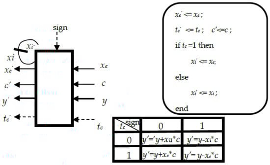
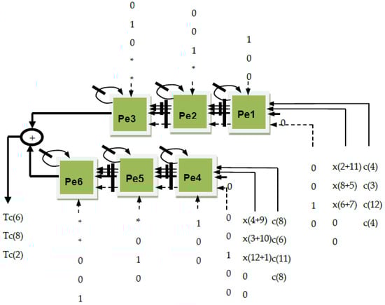
Figure 2.
The VLSI architecture of the hardware core that implements Equation (9), where * marks a delay of one clock cycle [26].
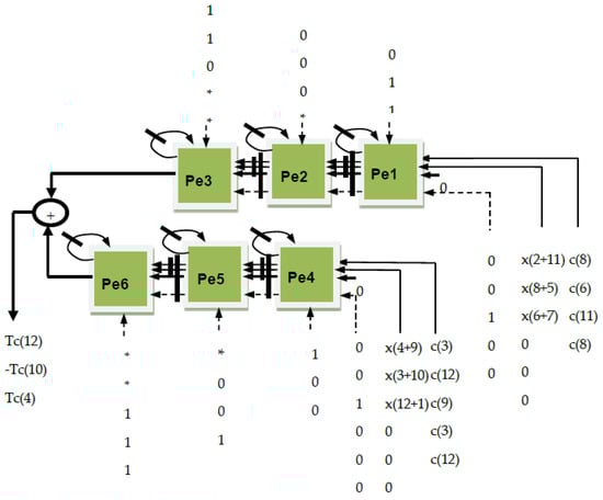
Figure 3.
The VLSI architecture of the hardware core that implements Equation (10), where * marks a delay of one clock cycle [26].
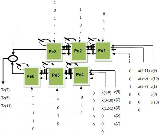
Figure 4.
The VLSI architecture of the hardware core that implements Equation (11), where * marks a delay of one clock cycle [26].
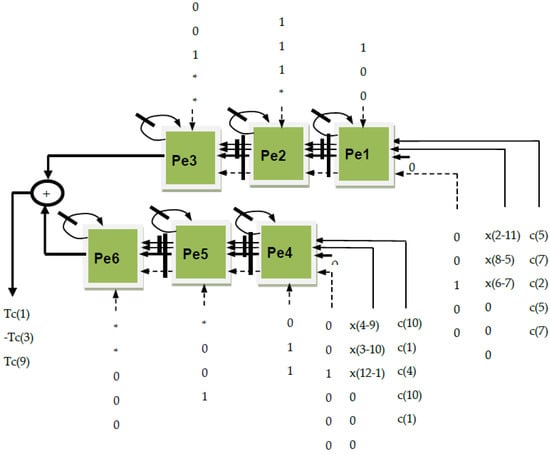
Figure 5.
The VLSI architecture of the hardware core that implements Equation (12), where * marks a delay of one clock cycle [26].
Figure 2, Figure 3, Figure 4 and Figure 5 present the architecture of the hardware core, which is implementing the reformulated algorithm; each systolic array implements Equations (9)–(12). Each systolic array shown below has 6 processing elements, which are grouped three by three, and any processing element contains a control bit and a corresponding multiplexer. The control bit is used for controlling the sign of the computations. Thus, the proposed architecture has 6 control bits for the 6 PEs and the technique of time-varying obfuscation is implemented by modifying the control bits; this way it has as a result multiple outputs, with one being the right one and the rest being obfuscated.
We can see in Figure 2, Figure 3, Figure 4 and Figure 5 that there are 6 short quasi-circular correlation structures and they all have a similar structure and of course the same length, which leads both to a I/O cutback and hardware cost reduction.
In Figure 2 we have mapped the data flow graph for Equation (9) and we have obtained the systolic array from below. We can see that the hardware core computes the auxiliary input sequences x(4 + 9), x(3 + 10), x(12 + 1), x(2 + 11), x(8 + 5) and x(6 + 7), and the auxiliary output Tc(6), Tc(8) and Tc(2) of the DCT-IV transform.
In Figure 3 we have mapped Equation (10) and we have obtained the systolic array from below. We can see that the hardware core computes the auxiliary input sequences x(4 + 9), x(3 + 10), x(12 + 1), x(2 + 11), x(8 + 5) and x(6 + 7), and the auxiliary output Tc(12), Tc(10) and Tc(4) of the DCT-IV transform.
In Figure 4 we have mapped Equation (11) from the VLSI algorithm of DCT-IV and we have obtained another systolic array. We can see that the hardware core computes the auxiliary input sequences x(4 − 9), x(3 − 10), x(12 − 1), x(2 − 11), x(8 − 5) and x(6 − 7), and the auxiliary output Tc(7), Tc(5) and Tc(11) of the DCT-IV transform.
In Figure 5 we have obtained another systolic array that implements Equation (12). We can see that the hardware core computes the auxiliary input sequences x(4 − 9), x(3 − 10), x(12 − 1), x(2 − 11), x(8 − 5) and x(6 − 7), and the auxiliary output Tc(1), Tc(3) and Tc(9) of the DCT-IV transform.
In addition to the hardware core, we need to mention the pre-processing and post-processing stages, which implement relations (7) and (8) and (4)–(6), respectively. They are needed to gather, from the input chain, the needed data in the required format and for recursively calculating the output.
2.4. VLSI Architecture for DST-IV
Figure 6 shows the functioning of a processing element from Figure 7, Figure 8, Figure 9 and Figure 10. It can be seen that it is the same with that given in Figure 1 for the VLSI architecture of type IV DCT. This is very important in view of obtaining a unified architecture resulting in having the same hardware core for the DCT-IV and DST-IV.
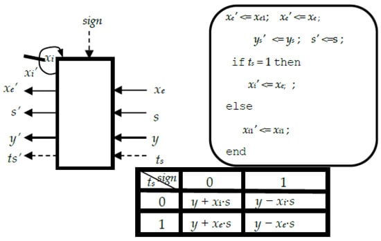
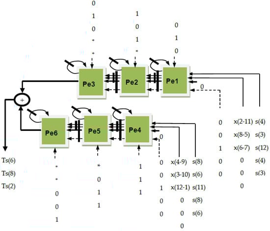
Figure 7.
The VLSI architecture of the hardware core that implements Equation (30), where * marks a delay of one clock cycle.

Figure 8.
The VLSI architecture of the hardware core that implements Equation (31), where * marks a delay of one clock cycle.

Figure 9.
The VLSI architecture of the hardware core that implements Equation (32), where * marks a delay of one clock cycle.
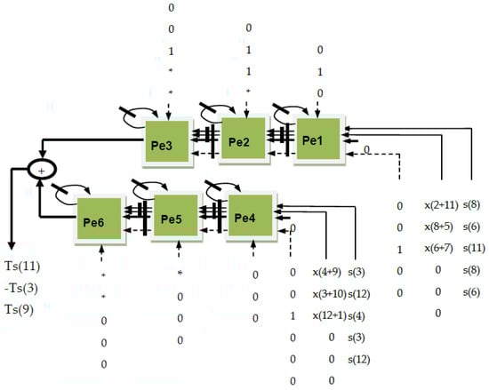
Figure 10.
The VLSI architecture of the hardware core that implements Equation (33), where * marks a delay of one clock cycle.
Similarly to the VLSI architecture for DCT-IV, we have the same 6 processing elements for each individual systolic array.
In Figure 7 we have mapped the data flow graph for Equation (30) and we have obtained the systolic array from below. We can see that the architecture presented computes the auxiliary output sequences Ts(2), Ts(8) and Ts(6), using the auxiliary input sequences x(4 − 9), x(3 − 10), x(12 − 1), x(2 − 11), x(8 − 5) and x(6 − 7) of the DST-IV transform.
In Figure 8 we have mapped the data flow graph for Equation (31) and we have obtained the systolic array from below. We can see that the architecture presented computes the auxiliary output sequences Ts(4), Ts(10) and Ts(12), using the auxiliary input sequences x(4 − 9), x(3 − 10), x(12 − 1) and x(2 − 11), x(8 − 5), x(6 − 7) of the DST-IV transform.
In Figure 9 we have mapped the data flow graph for Equation (32) and we have obtained another systolic array. We can see that the architecture presented is computing the auxiliary output sequences Ts(11), Ts(5) and Ts(7), using the auxiliary input sequences x(4 + 9), x(3 + 10), x(12 + 1), x(2 + 11), x(8 + 5) and x(6 + 7) of the DST-IV transform.
In Figure 10 we have mapped Equation (33), resulting in the systolic array from below. We can see that the architecture presented computes the auxiliary output sequences Ts(9), Ts(3) and Ts(1), using the auxiliary input sequences x(4 + 9), x(3 + 10), x(12 + 1), x(2 + 11), x(8 + 5) and x(6 + 7) of the DST-IV transform.
3. Results
Figure 11 shows the principle of the time-varying obfuscation technique that was used for our unified VLSI architecture, where the right key values are represented by K[0...5], the trigger signal is noted with Ti, the obfuscated signal is noted with Ci, and G represents the combination between Ti and Ci, thus obtaining the obfuscated signal. We have noted, with C1c, …, C6c, the correct sign bits for DCT-IV and, with C1s, …, C6s, the correct sign bits for DST-IV. The right signal is achieved at x1 and x6, when K[0] = 0, K[1] = 0, K[2] = 1, K[3] = 0, K[4] = 0 and K[5] = 1, whilst for the rest, erroneous signals are selected. The combination formed by K[0], …, K[5] represents the obfuscation key.
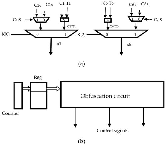
Figure 11.
(a) Time-varying obfuscation. (b) Obfuscation circuit.
Figure 11b presents the obfuscation scheme and Figure 12 presents the functioning of a processing element PE that we have used in our unified VLSI architecture given in Figure 13, Figure 14, Figure 15 and Figure 16. As shown in Figure 10, for each processing element, we have three control tags that are rotated. To select the correct control tags in Figure 13, Figure 14, Figure 15 and Figure 16, we need a key[0…2] for the systolic array from above, and a key[3…5] for the systolic array from below. However, as there are three control tags for each processing element that is rotated, we need three keys that also have to be rotated, as in Figure 11b. This leads to a more difficult task when attempting to identify the correct sequence of keys. This obfuscation scheme has not been used until now.
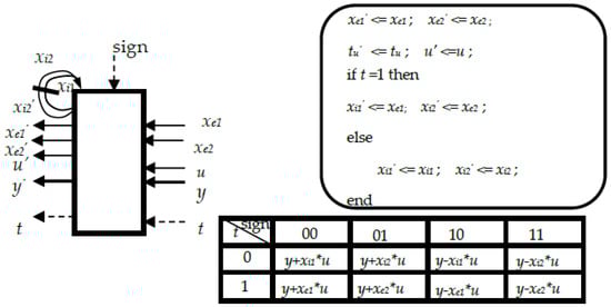
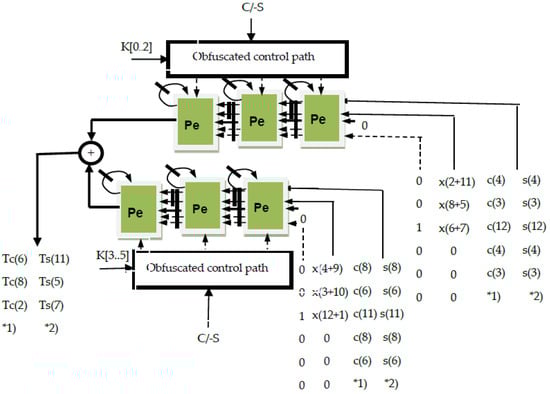
Figure 13.
The unified VLSI architecture for DCT/DST-IV based on the unified algorithm for Equations (9) and (32) where *1) represents the cosine entry that is in parallel with *2) the sine entry; the correct entry is selected depending on the pre-processing stage to calculate what is needed (DCT-IV or DS-IV).
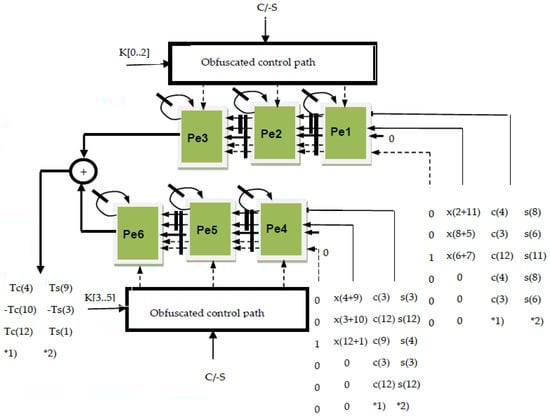
Figure 14.
The unified VLSI architecture for DCT/DST-IV based on the unified algorithm for Equations (10) and (33) where *1) represents the cosine entry that is in parallel with *2) the sine entry; the correct entry is selected depending on the pre-processing stage to calculate what is needed (DCT-IV or DST-IV).
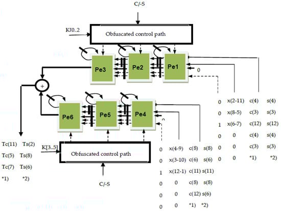
Figure 15.
The unified VLSI architecture for DCT/DST-IV based on the unified algorithm for Equations (11) and (30) where *1) represents the cosine entry that is in parallel with *2) the sine entry; the correct entry is selected depending on the pre-processing stage to calculate what is needed (DCT-IV or DST-IV).
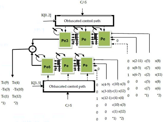
Figure 16.
The unified VLSI architecture for DCT/DST-IV based on the unified algorithm for Equations (12) and (29) where *1) represents the cosine entry that is in parallel with *2) the sine entry; the correct entry is selected depending on the pre-processing stage to calculate what is needed (DCT-IV or DST-IV).
Next, we will show how we obtain the unified VLSI array for DCT-IV and DST-IV, which allows the integration of the obfuscation scheme presented above.
In Section 2.1 and Section 2.3, we have presented the VLSI algorithm for DCT-IV, and its VLSI architecture that efficiently includes the obfuscation technique [25]. The VLSI algorithm uses eight short pseudo-circular correlations that can be computed in parallel, and thus we can obtain high-speed performances using parallelism. The proposed VLSI algorithm has been implemented using the systolic array paradigm that allows low hardware complexity to be obtained. The obtained VLSI architecture can efficiently incorporate the obfuscation technique, and it has a good topology with local and regular interconnections that allow efficient VLSI implementation.
In Section 2.2 and Section 2.4, we have presented a new VLSI algorithm for DST-IV and its VLSI architecture that also allows the efficient inclusion of the obfuscation technique. The obtained VLSI algorithm also uses eight short pseudo-circular correlations that can be computed in parallel and has a similar structure as that obtained for DCT-IV, thus enabling efficient unified implementation of the two transforms on the same hardware core, with very few modifications in the pre-processing and post-processing stages.
As can be seen from Figure 13, Figure 14, Figure 15 and Figure 16, we can efficiently unify the architectures for the computation of DCT-IV with those for DST-IV, using the proposed VLSI algorithms and architectures. Thus, we can unify the architecture that computes Tc(6), Tc(8) and Tc(3) of the DCT-IV algorithm with the architecture that computes Ts(11), Ts(5) and Ts(7) for DST-IV. It is apparent that we can use the same architecture for both of the transforms, and we only have to change the sign bits and the cosine/sine coefficients. It can be seen that the auxiliary input sequences x(2 + 11), x(8 + 5), x(6 + 7), x(4 + 9), x(3 + 10) and x(12 + 1) do not change when we switch the computation from DCT-IV to DST-IV.
In Figure 13, we have the systolic array that implements Equations (9) and (30) in a unified manner. As can be seen, we can compute the auxiliary outputs Tc(7), Tc(5) and Tc(11) of the DCT-IV sequences, and Ts(6), Ts(8) and Ts(2) for DST-IV, using the same hardware, without any modifications. We have to switch the input sequences with the sine and cosine coefficients noted in Figure 13, with *1) and *2) and the sign bits noted with *1) for DCT-IV and *2) for DST-IV, which are different in the computation of the two transforms.
We can also unify the architecture that computes Tc(4), Tc(10) and Tc(12) of the DCT-IV algorithm with the architecture that computes Ts(9), Ts(3) and Ts(1) for DST-IV. It can be seen that we can use the same architecture for both of the transforms and we only have to change the sign bits and the cosine/sine coefficients. The auxiliary input sequences x(2 + 11), x(8 + 5), x(6 + 7), x(4 + 9), x(3 + 10) and x(12 + 1) do not change when we switch the computation from DCT-IV to DST-IV. In Figure 14, we have the systolic array that implements Equations (1) and (20) in a unified manner. As shown in Figure 14, we can compute the auxiliary output sequences Tc(4), Tc(10) and Tc(12) of DCT-IV, and Ts(9), Ts(3) and Ts(1) for DST-IV, using the same architecture, without any modifications in the hardware. We have to switch the input sequences with the sine and cosine coefficients noted in Figure 14, with *1) and *2) and the sign bits noted with *1) for DCT-IV and *2) for DST-IV, which are different in the computation of the two transforms.
We can then unify the architecture that computes Tc(7), Tc(5) and Tc(11) of the DCT-IV algorithm with the architecture that computes Ts(6), Ts(8) and Ts(2) for DST-IV. As in the previous cases, it can be seen that we can use the same architecture for both of the transforms, and we only have to change the sign bits and the cosine/sine coefficients. It can be seen that the auxiliary input sequences x(2 − 11), x(8 − 5), x(6 − 7), x(4 − 9), x(3 − 10) and x(12 − 1) do not change when we switch the computation from DCT-IV to DST-IV. In Figure 16, we have obtained the unified systolic array that implements Equations (11) and (32) in a unified manner. As shown in Figure 16, we can compute the auxiliary outputs Tc(7), Tc(5) and Tc(11) of the DCT-IV sequences, and Ts(6), Ts(8) and Ts(2) for DST-IV using the same hardware, without any modifications. We have to switch the sequences with the sine and cosine coefficients noted in Figure 16, with *1) and *2) and the sign bits, which are different in the computation of the two transforms.
We can then unify the architecture that computes Tc(1), Tc(3) and Tc(9) of the DCT-IV algorithm with the architecture that computes Ts(12), Ts(10) and Ts(4) for DST-IV. As in the previous cases, it can be seen that we can use the same architecture for both of the transforms, and we only have to change the sign bits and the cosine/sine coefficients. The auxiliary input sequences x(2 − 11), x(8 − 5), x(6 − 7), x(4 − 9), x(3 − 10) and x(12 − 1) do not change when we switch the computation from DCT-IV to DST-IV. In Figure 16, we have the systolic array that implements Equations (12) and (33) in a unified manner. Also, as can be seen in Figure 16, we can compute the auxiliary outputs Tc(1), Tc(3) and Tc(9) of the DCT-IV sequences, and Ts(12), Ts(10) and Ts(4) for DST-IV using exactly the same hardware. We have to switch the sequences with the sine and cosine coefficients noted in Figure 16, with *1) and *2) and the sign bits, which are different in the computation of the two transforms.
We can see that we can use the same hardware in the post-processing stage to compute Equation (3) for DCT-IV and (24) for DST-IV, but only changing the sequences of the sine and cosine coefficients. Also, Equations (4) and (5) for DCT-IV, and (25) and (26) for DST-IV can be computed in the post-processing stage, using the same hardware, without any modifications.
We can also use almost the same hardware to compute the auxiliary input sequences, using Equations (7) and (8) for DCT-IV, and (28) and (29) for DST-IV; the only difference is in one sign.
4. Discussion
We have obtained two VLSI algorithms and architectures for type IV DCT and type IV DST that allow for an efficient unified VLSI implementation and an efficient incorporation of the obfuscation technique, with very low overheads.
4.1. Evaluation of the Results
In our analysis, we start with the following observation: It is not possible to extract the correct bits of the key applied to each MUX if the whole simulation is not finished. If we have an MUX with M input signals and one output of type L:1, where M is the number of control signals, then the total number of combinations is LM, out of which only one is correct.
If we consider, for example, Figure 9, we have three control bits for the systolic array from above and another three control bits for the array below. For each combination of bits, we have one key. However, we have to use three keys that are circulated in a cycle manner, with the length of the sequence equal with three. These three keys have to be applied in the right sequence. The number of permutations is three! Moreover, only one sequence is correct.
Thus, the number of functional modes, N, which is also showcased in Table 2, will be equal with (3!L3)(3!L3), out of which only one mode is correct. For L = 4, we have N = 147,456 of modes, but only one is correct and yields the correct result. However, we have four such VLSI architectures that each give 25% of the result. So, for one correct result, we have N4 − 1 modes that yield a wrong result.
Table 2.
Analysis of functional modes.
The proposed unified VLSI architecture allows efficient implementation of the obfuscation technique to be obtained, due to the control bits introduced that can be efficiently used, as it can be seen in Figure 7, Figure 8, Figure 9 and Figure 10.
The overhead area of the proposed obfuscation scheme consists of 48 MUXs and 24 AND gates, and is less than 0.5% of the total chip area.
The overheads determined by the unification of the two VLSI architectures are very low. As we compare the equations of the two transforms, we can see that there is one difference in the sign of Equations (8) and (29) that affects the hardware structure. The rest of the differences only affect the input sequences and not the hardware structure. So, the unification overheads are really very small, being less than 0.01% of the chip area.
In the proposed VLSI architectures, we have 2(N − 1) multipliers and 2(N − 1) adders, and we obtain four output samples for each clock cycle. The result is obtained after (N − 1)/4 clock cycles. As can be seen before, for the two VLSI algorithms, we have obtained two VLSI architectures with very good performances, such as high-speed processing, using a parallel decomposition of the two VLSI algorithms, and thus obtaining low hardware complexity and a good topology that allows efficient VLSI implementation.
4.2. Comparison
We will compare our VLSI architecture with some of the most relevant VLSI implementations for DCT-IV and DST-IV, to show that we can embed the obfuscation technique without affecting the performances of VLSI implementation. It was also shown that the proposed approach allows efficient embedding of the obfuscation technique with a low area/power and zero performance overheads.
As compared with existing VLSI architectures for DCT-IV and DST-IV, we can see that in [28,29] the throughput is four times lower as compared with our proposed solution, where we have eight systolic arrays working in parallel rather than two systolic arrays, as in [28,29]. Moreover, the solution proposed in [31] is dedicated to DCT-IV and neither one of them incorporate the obfuscation technique.
In [32,33,34,35,36,37,38,39], we see a hardware accelerator for the computation of DCT-IV. In the proposed method, each data from the input sequence is fed to a multiplier and to an accumulator. The partial results are recursively computed until the output sample is obtained after N clock cycles. The proposed hardware accelerator contains 3N registers, 2N adders and 2N multipliers, as opposed to our VLSI implementation that contains 2(N − 1) multipliers and 2(N − 1) adders. We obtain four output samples each clock cycle, as opposed to [25], where we obtain eight output samples after eight clock cycles. Moreover, the VLSI architecture from [25] is difficult to unify and is not possible to include the obfuscation technique, as there are no control bits.
As compared to [5], we have the same number of multipliers and adders 2(N − 1)/2 as in our VLSI architectures, and the same throughput, but the VLSI architecture in [5] is dedicated to DCT-IV and cannot be used to efficiently incorporate the obfuscation technique, due to the absence of control bits. Comparing to [5], we obtain the same performance with an addition of a cost increase for the hardware, which is caused by the addition of the multiplexers needed for implementing the obfuscation.
As compared with our paper presented at TSP 2020 [26], which was extended in this article, the proposed solution represents a unified approach based on a unified VLSI algorithm that allows a unified VLSI architecture for DCT/DST-IV that grants efficient incorporation of the obfuscation technique. We have used another obfuscation technique that circulates a sequence of security keys, which renders the detection of the correct sequence of keys more difficult, and that allows the obfuscation technique to be embedded with a low area/power and zero performances overhead, while maintaining the high performances of the VLSI implementation of DCT/DST-IV.
As was shown in Section 4.1 and Section 4.2, it is possible to efficiently unify the two VLSI architectures for computing DCT-IV and DST-IV, while incorporating an efficient obfuscation technique with low area overheads and no performances overhead, and obtaining, at the same time, a low area/power and high performances. Future work will include the implementation of the algorithm on an FPGA.
5. Conclusions
In this paper, we have extended the design approach presented by us at the TSP 2020 [26]. The proposed method uses regular and modular structures named quasi-circular correlations, in order to obtain a unified VLSI architecture for type IV DCT/DST. It has high performances and it attains hardware security with very low overheads. We have included the obfuscation technique in the unified VLSI architecture of DCT/DST-IV with very low area/power overheads and zero performances overhead. The high-speed performances have been obtained by using parallelism and pipelining with a low hardware complexity, and a good topology with local connections, obtaining an architecture that is well suited for VLSI implementation; the architecture is inspired by the paradigm of the systolic array architecture, which allows efficient VLSI implementation. The algorithms and architectures for the two transforms were restructured in such a manner that they can be implemented on the same VLSI chip, using the same hardware, with very few modifications in the pre-processing and post-processing stages. Thus, we have the added benefit of attaining hardware security with very low overheads and obtaining, at the same time, very efficient VLSI implementation.
The main limitation of the paper is the use of an approach that is an extension of the static obfuscation technique, and as future directions of the research, we can mention the use of the time-varying obfuscation technique and the extension of the research for other DSP algorithms.
Author Contributions
Conceptualization, D.F.C.; methodology, D.F.C. and L.-T.C.; software, D.F.C. and L.-T.C.; validation, D.F.C. and L.-T.C.; formal analysis, D.F.C. and L.-T.C.; investigation, D.F.C. and L.-T.C.; resources, D.F.C.; data curation, D.F.C. and L.-T.C.; writing—original draft preparation, D.F.C. and L.-T.C.; writing—review and editing, D.F.C., and L.-T.C.; visualization, D.F.C. and L.-T.C.; supervision, D.F.C.; project administration, D.F.C.; funding acquisition, D.F.C. All authors have read and agreed to the published version of the manuscript.
Funding
This work was supported by a grant of the Romanian Ministry of Education and Research, CNCS—UEFISCDI, project number PCE 172/2021 (PN-III-P4-ID-PCE2020-0713), within PNCDI III.
Acknowledgments
The authors would like to thank the Romanian Ministry of Education and Research for their support in offering the grant CNCS—UEFISCDI, project number PCE 172/2021 (PN-III-P4-ID-PCE2020-0713), within PNCDI III.
Conflicts of Interest
The authors declare no conflict of interest.
References
- Jain, A.K. A sinusoidal family of unitary transforms. IEEE Trans. Pattern Mach. Intell. 1979, PAMI-1, 365. [Google Scholar] [CrossRef] [PubMed]
- Jing, C.; Tai, H.-M. Fast algorithm for computing modulated lapped transform. Electron. Lett. 1979, 37, 796–797. [Google Scholar] [CrossRef]
- Malvar, H.S. Lapped transforms for efficient transforms/subband coding. IEEE Trans. Acoust. Speech Signal Process. 1990, 38, 969–978. [Google Scholar] [CrossRef]
- Malvar, H.S. Signal Processing with Lapped Transforms; Artech House: Norwood, MA, USA, 1991. [Google Scholar]
- Chiper, D.F. A new VLSI algorithm for a high-throughput implementation of type IV DCT. In Proceedings of the 2016 International Conference on Communications (COMM), Bucharest, Romania, 9–10 June 2016. [Google Scholar]
- Pilato, C.; Garg, S.; Wu, K.; Karri, R.; Regazzoni, F. Securing hardware accelerators: A new challenge for high-level synthesis. IEEE Embedded Syst. Lett. 2018, 10, 77–80. [Google Scholar] [CrossRef]
- Kayes, A.S.M.; Kalaria, R.; Sarker, I.H.; Islam, M.S.; Watters, P.A.; Ng, A.; Hammoudeh, M.; Badsha, S.; Kumara, I. A Survey of Context-Aware Access Control Mechanisms for Cloud and Fog Networks: Taxonomy and Open Research Issues. Sensors 2020, 20, 2464. [Google Scholar] [CrossRef]
- Knechtel, J.; Patnaik, S.; Sinanoglu, O. Protect your chip design intellectual property: An overview. In Proceedings of the International Conference on Omni-Layer Intelligent Systems, Crete, Greece, 5–7 May 2019; pp. 211–216. [Google Scholar]
- Parhi, K.K.; Koteshwara, S. Dynamic Functional Obfuscation. U.S. Patent 15/667 776, 3 August 2017. [Google Scholar]
- Zhang, J. A practical logic obfuscation technique for hardware security. IEEE Trans. Very Large Scale Integr. (VLSI) Syst. 2016, 24, 1193–1197. [Google Scholar] [CrossRef]
- Chen, S.; Chen, S.; Wang, L. A chip-level anti-reverse engineering technique. J. Emerg. Technol. Comput. Syst. 2018, 14, 1–20. [Google Scholar] [CrossRef]
- Shamsi, K.; Li, M.; Meade, T.; Zhao, Z.; Pan, D.Z.; Jin, Y. AppSAT: Approximately deobfuscating integrated circuits. In Proceedings of the 2017 IEEE International Symposium on Hardware Oriented Security and Trust (HOST), Mclean, VA, USA, 1–5 May 2017. [Google Scholar]
- Sengupta, A.; Roy, D.; Mohanty, S.P.; Corcoran, P. Low-cost obfuscated JPEG CODEC IP core for secure CE hardware. IEEE Trans. Consum. Electron. 2018, 64, 365–374. [Google Scholar] [CrossRef]
- Koteshwara, S.; Kim, C.H.; Parhi, K.K. Key-Based Dynamic Functional Obfuscation of Integrated Circuits Using Sequentially Triggered Mode-Based Design. IEEE Trans. Inf. Forensics Secur. 2018, 13, 79–93. [Google Scholar] [CrossRef]
- Koteshwara, S.; Kim, C.H.; Parhi, K.K. Hierarchical functional obfuscation of integrated circuits using a mode-based approach. In Proceedings of the 2017 IEEE International Symposium on Circuits and Systems (ISCAS), Baltimore, MD, USA, 28–31 May 2017. [Google Scholar]
- Xie, J.; Meher, P.K.; He, J. Hardware-Efficient Realization of Prime-Length DCT Based on Distributed Arithmetic. IEEE Trans. Comput. 2013, 62, 1170–1178. [Google Scholar] [CrossRef]
- Perera, S.M. Signal flow graph approach to efficient and forward stable DST algorithms. Linear Algebra Appl. 2018, 542, 360–390. [Google Scholar] [CrossRef]
- Koteshwara, S.; Kim, C.H.; Parhi, K.K. Mode-based Obfuscation using Control-Flow Modifications. In Proceedings of the Third Workshop on Cryptography and Security in Computing Systems, Prague, Czech Republic, 20 January 2016. [Google Scholar]
- Chiper, D.F. A new systolic array algorithm for memory-based VLSI array implementation of DCT. In Proceedings of the Second IEEE Symposium on Computer and Communications, Alexandria, Egypt, 1–3 July 1997. [Google Scholar]
- Yu, S.; Swartzlander, E.E. DCT Implementation with Distributed Arithmetic. IEEE Trans. Comput. 2001, 50, 985–991. [Google Scholar]
- Kim, D.W.; Kwon, T.W.; Seo, J.M.; Yu, J.K.; Lee, S.K.; Suk, J.H.; Choi, J.R. A compatible DCT/IDCT architecture using hardwired distributed arithmetic. In Proceedings of the 2001 IEEE International Symposium on Circuits and Systems (Cat. No.01CH37196), Sydney, NSW, Australia, 6–9 May 2001. [Google Scholar]
- Madisetti, A.; Wilson, A.N. A 100 Mhz 2-D 8 × 8 DCT/IDCT processor for HDTV applications. IEEE Trans. Circuits Syst. Video Technol. 1995, 5, 158–165. [Google Scholar] [CrossRef]
- Chiper, D.F.; Swamy, M.N.S.; Ahmad, M.O. An Efficient Unified Framework for the VLSI Implementation of a Prime-Length DCT/IDCT with High Throughput. IEEE Trans. Signal Process. 2007, 55, 2925–2936. [Google Scholar] [CrossRef]
- Hsiao, S.F.; Shiue, W.R.; Tseng, J.M. Design and implementation of a novel linear array DCT/IDCT processor with complexity of order. IEEE Proc. Vis. Images Signal Process. 2000, 147, 400–408. [Google Scholar] [CrossRef]
- Lai, S.-C.; Chien, W.-C.; Lan, C.-S.; Lee, M.-K.; Luo, C.-H.; Lei, S.-F. An efficient DCT-IV-based ECG compression algorithm and its hardware accelerator design. In Proceedings of the 2013 IEEE International Symposium on Circuits and Systems (ISCAS), Beijing, China, 19–23 May 2013. [Google Scholar]
- Cotorobai, L.-T.; Chiper, D.F. A New VLSI Algorithm for type IV DCT for an Efficient Implementation of Obfuscation Technique. In Proceedings of the 2020 43rd International Conference on Telecommunications and Signal Processing (TSP), Milan, Italy, 7–9 July 2020. [Google Scholar]
- Kidamni, S.S. Recursive Implementation of the DCT-IV and DST-IV. In Proceedings of the 1998 IEEE Symposium on Advances in Digital Filtering and Signal Processing. Symposium Proceedings (Cat. No.98EX185), Victoria, BC, Canada, 5–6 June 1998. [Google Scholar]
- Sengupta, A.; Roy, D.; Mohanty, S.P.; Corcoran, P. DSP design protection in CE through algorithmic transformation based structural obfuscation. IEEE Trans. Consum. Electron. 2017, 63, 467–476. [Google Scholar] [CrossRef]
- Perera, S.M.; Liu, J. Complexity reduction, self/completely recursive, radix-2 DCT I/IV algorithms. J. Comput. Appl. Math. 2020, 379, 112936. [Google Scholar] [CrossRef]
- Lao, Y.; Parhi, K.K. Obfuscating DSP Circuits via High-Level Transformations. IEEE Trans. Very Large Scale Integr. (VLSI) Syst. 2014, 23, 819–830. [Google Scholar] [CrossRef]
- Chakraborty, R.S.; Bhunia, S. Security against hardware Trojan through a novel application of design obfuscation. In Proceedings of the 2009 IEEE/ACM International Conference on Computer-Aided Design—Digest of Technical Papers, San Jose, CA, USA, 2–5 November 2009. [Google Scholar]
- Luo, C.-H.; Ma, W.-J.; Juang, W.-H.; Kuo, S.-H.; Chen, C.-Y.; Tai, P.-C.; Lai, S.-C. An ECG Acquisition System Prototype Design with Flexible PDMS Dry Electrodes and Variable Transform Length DCT-IV Based Compression Algorithm. IEEE Sens. J. 2016, 16, 8244–8254. [Google Scholar] [CrossRef]
- Chen, Z.; Han, Q.; Cham, W.K. Low-Complexity Order-64 Integer Cosine Transform Design and Its Application in HEVC. IEEE Trans. Circuits Syst. Video Technol. 2018, 28, 2407–2412. [Google Scholar] [CrossRef]
- Meher, P.K. Systolic designs for DCT using low-complexity concurrent convolutional formulation. IEEE Trans. Circuits Syst. Video Technol. 2006, 16, 1041–1050. [Google Scholar] [CrossRef]
- Chiper, D.F.; Ungureanu, P. Novel VLSI Algorithm and Architecture with Good Quantization Properties for a High-Throughput Area Efficient Systolic Array Implementation of DCT. EURASIP J. Adv. Signal Process. 2011, 2011, 639043. [Google Scholar] [CrossRef]
- Chiper, D.F.; Cotorobai, L.T. A New VLSI Algorithm for an Efficient VLSI Implementation of Type IV DST based on Short Band-Correlation Structures. In Proceedings of the 2020 13th International Conference on Communications (COMM), Bucharest, Romania, 18–20 June 2020. [Google Scholar]
- Murphy, N.R.; Swamy, M.N.S. On the On-Line Computation of DCT-IV and DST-IV Transforms. IEEE Trans. Signal Process. 1995, 43, 1249–1251. [Google Scholar] [CrossRef]
- Chiper, D.F.; Ahmad, M.O.; Swamy, M.N. A Unified VLSI Algorithm for a High Performance Systolic Array Implementation of Type IV DCT/DST. In Proceedings of the International Symposium on Signals, Circuits and Systems ISSCS2013, Iasi, Romania, 11–12 July 2013. [Google Scholar]
- Chiper, D.F. An Efficient Algorithm for a Memory-Based Systolic Array VLSI Implementation of Type IV DCT. In Proceedings of the 2015 International Symposium on Signals, Circuits and Systems (ISSCS), Iasi, Romania, 9–10 July 2015. [Google Scholar]
Publisher’s Note: MDPI stays neutral with regard to jurisdictional claims in published maps and institutional affiliations. |
© 2021 by the authors. Licensee MDPI, Basel, Switzerland. This article is an open access article distributed under the terms and conditions of the Creative Commons Attribution (CC BY) license (https://creativecommons.org/licenses/by/4.0/).