1. Introduction
Due to the rapid development of power semiconductor and computing technology, the structures of electrical equipment have changed in recent decades, and great efforts are being made to produce these sophisticated devices with high efficiency and the necessary dimensions and effects [
1,
2,
3].
Nowadays, in large electronic devices, the power supply is realized as a switched-mode power supply. A diode rectifier is usually used at the input, followed by a filter capacitor, which allows the AC voltage to be transfered to a DC voltage. An input rectifier with capacitive filter taken from the distribution network of pulse currents, leads to the consumption of higher harmonic components of the current, which adversely affects other equipment on the distribution network. As a result, we started using active rectifiers—power factor correction. Today, every manufacturer is trying to reduce the volume of the inverter that is connected to the mains in order to optimize the dimensions and weight. One of the ways to reduce the converter itself is to optimize it for higher switching frequencies, through which it is possible to use passive elements with smaller values and thus smaller dimensions [
4,
5,
6,
7].
However, the ability to operate at high switching frequencies is limited by the switching speed of the transistor, as it is important to maintain relatively low switching losses. At present, from an economic or functional point of view, SiC technology appears to be the most widely used transistor technology in industrial power supplies. Transistors of this technology are manufactured up to a voltage of 1700 V and are able to operate up to a frequency of 200 kHz at several kW of inverter power. Nowadays, however, GaN technology is also beginning to be used in industrial power supplies, which promises a significant increase in switching frequency with relatively small switching losses. The previous problem was mainly the absence of high voltage GaN transistors (650–1200 V), which would be applicable to three-phase PFC sources connected to the European network [
8].
The main goal of this work is to implement and evaluate the switching performance of the latest transistor technologies (SiC and GaN) within the industrially used PFC converter. This aim targets the optimization of the selected converter considering the efficiency characteristic as well as power density optimization. Regarding the power density, it is related to the verification of the operation of selected transistor structures at high-frequency operation (from 120 kHz up to 250 kHz), while the original switching frequency was only 41 kHz. This significant increase in switching frequency enables us to further optimize PFC inductances, which represents the main component of the selected topology of PFC.
From a scientific point of view, this approach represents the investigation of the posibilities of how to improve the power density of modern power semiconductor converters, while maintaining a very high efficiency performance within a wide power range. This issue also adresses the requirements regarding the optimization of the inductive components due to a multiple increase in the operational frequency. As the above-mentioned claims represent a complex task, the main focus here is on the investigation of the optimization process in the utilization of modern power semiconductor transistors within the main circuit of a three-phase dual interleaved PFC converter.
2. Materials and Methods
Continuous development in the field of power semiconductors is leading power electronic systems to new dimensions characterized by improved efficiency, power density, and thermal performance. All these aspects are related to relationships that must be conceived in the form of a compromise during development. One of the ways to optimize solutions is through the research and development of a completely new system. Another way is the substitution of the main components and parts of the existing system using new technological materials and structures. In this work, we are discussing the upcoming trend where silicon power transistors are continuously substituted with the proposed components based on SiC and GaN technology. The process should be simple, just exchanging part for part, but several solutions require additional modification to the circuit, thus making the process more complex and costly. Because most of the switched mode power supplies require power factor correction, it is worth considering the efficiency performance of this system overall. Currently, SiC transistors are popular for modern PFC circuits; however, there is also GaN technology, which should undergo investigation as to whether it is a better solution for improving the operational characteristics of PFC itself [
9].
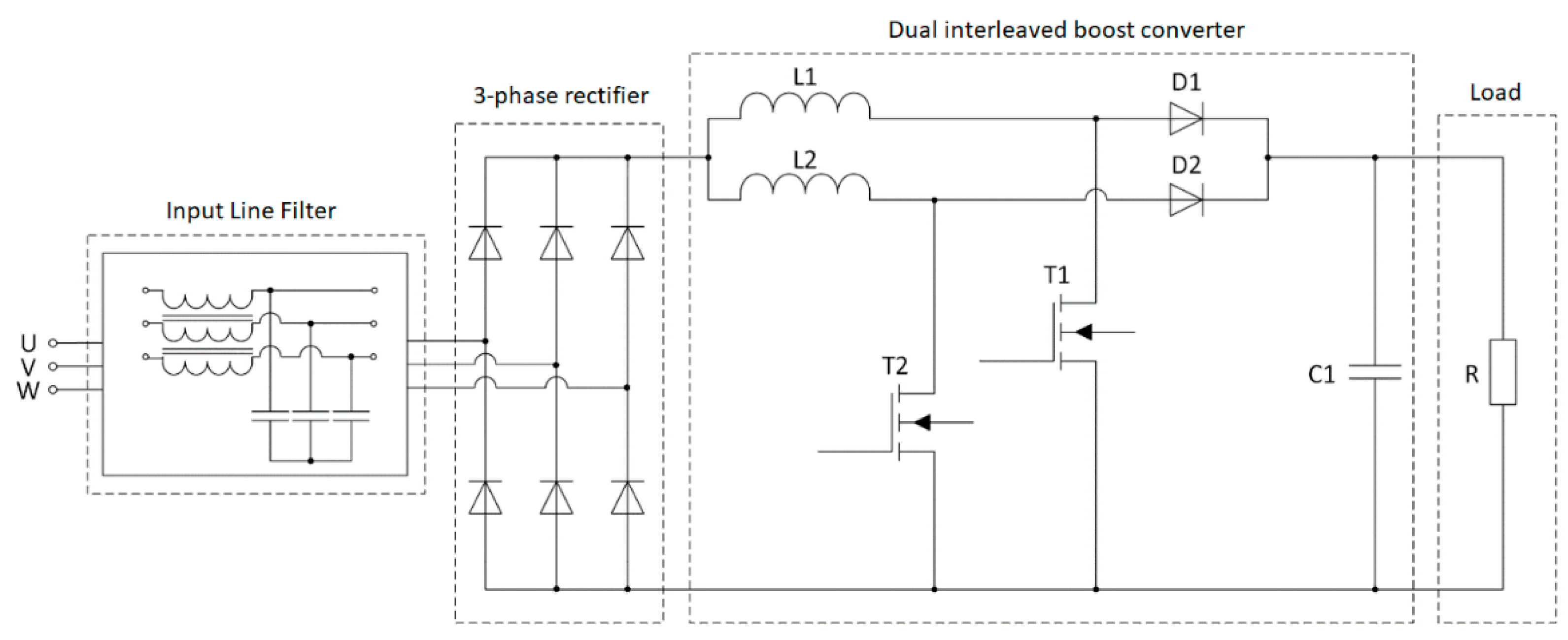
The target power semiconductor system is represented by a three-phase PFC converter, the principal schematics of which is shown on
Figure 1. This PFC type is based on the topology of an interleaved boost converter supplied by a non-controlled three-phase rectifier.
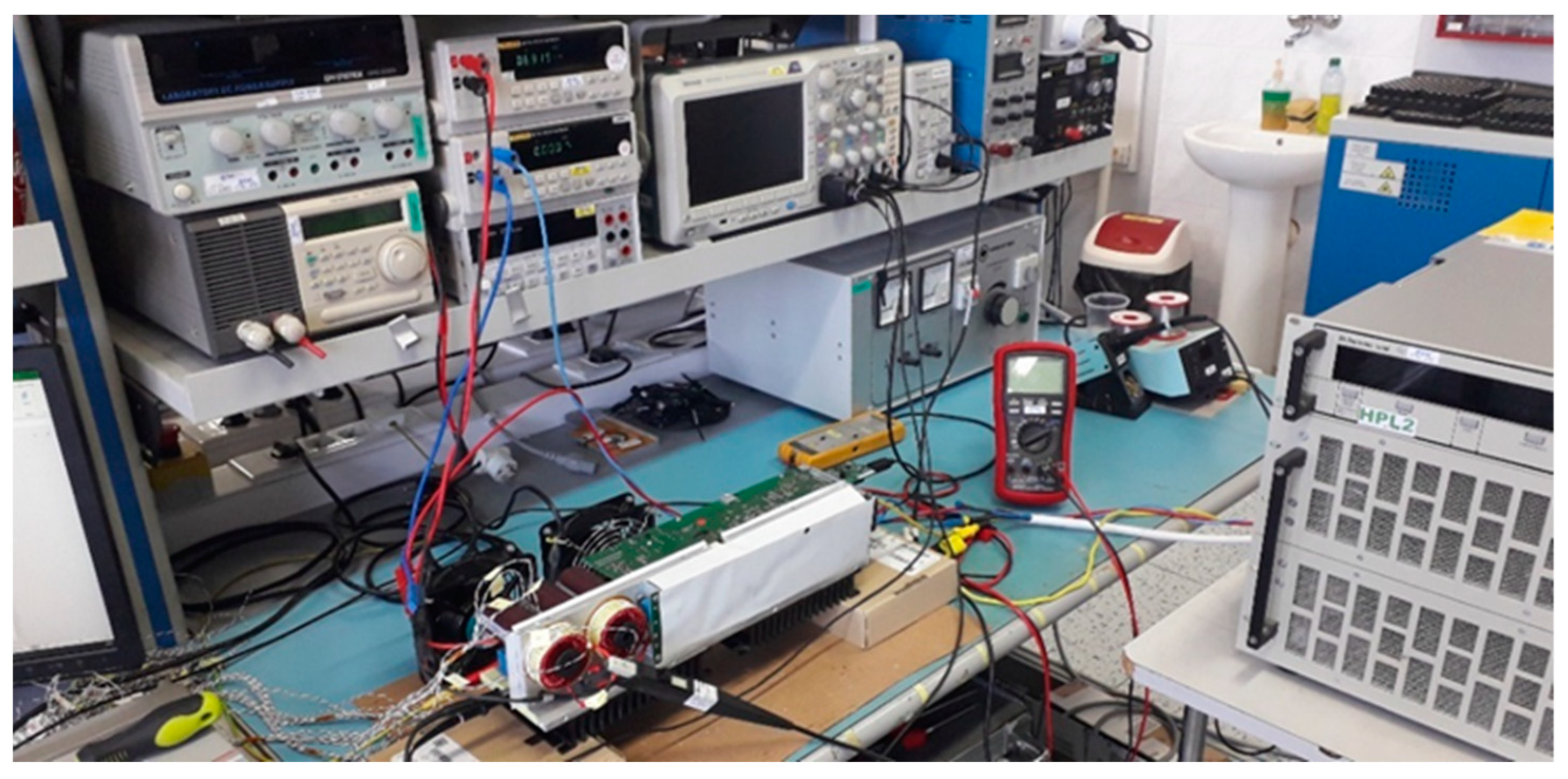
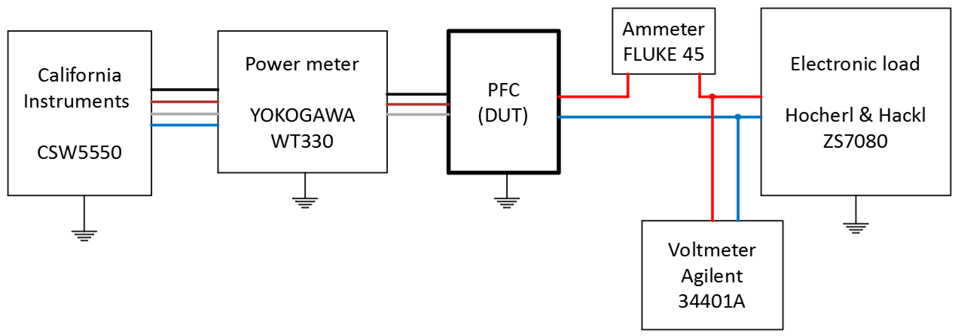
The testing procedure was achieved under laboratory conditions (
Figure 2). Experimental measurements were performed with calibrated laboratory equipment from renowned manufacturers such as Tektronix, California Instruments, Agilent and Fluke, Hocherl & Hackl, etc. Block diagrams of the experimental testing and measurements are shown in
Figure 3.
As an input source of the tested power converter, a three-phase supply grid was used. The change in the output power was performed by electronic load Hocherl & Hackl ZS7080. Because during the experimental testing of individual transistors, the switching frequency was also one of the variables, it was modified using a microprocessor controller. Measurement related to the efficiency evaluation was done in recoding effective values of the input and output variables, i.e., voltages and currents. This was performed by Fluke 45 (output ammeter) and Agilent 34401A (output voltmeter). Time waveforms were recorded with the use of the oscilloscope Textronix MDO3014 equipped with voltage and current probes from Tektronix. A list of the laboratory equipment used is given in
Table 1, while a block diagram of an experimental test-stand is shown in
Figure 3.
Because an important part acting as a source of power losses in PFC converters is represented by inductors, we considered the various construction (winding organization, air gap implementation) and material properties of inductors during the transistor evaluation as well.
The original solution of the PFC inductor was made on toroidal alloy core, which is suitable for an operational frequency up to 100 kHz. The switching frequency of the original solution of the PFC converter was 41 kHz, while the parameters and circuit components are listed in
Table 2.
As one of the main goals is the practical utilization of the new proposed transistor structures for industrial use, while maintaining high-efficiency operation together with high switching operation/improving power density, we were required to design and construct power inductors of the original PFC converter to operational conditions characterized by high-frequency operation. Modified inductors for high-frequency operation are made on toroidal ferrite core R50/30/20. Specific to these inductors is the implementation of a distributed airgap (
Figure 4) in order to reduce the effect of the fringing flux. These inductors have been verified for a switching frequency within 120 kHz up to 250 kHz, while the main parameters for the design and construction are given in
Table 3.
2.1. Proposed Power Transistor Structures for Selected Three-Phase PFC Converter
Currently, the commercial market for electronic power systems dispose of two of the most important material technologies regarding semiconductors, i.e., galium nitride and silicon carbide. Both structures belong to wide-bandgap semiconductor materials, while the semiconductors made of these materials are defined as composed components because they are composed of several elements from the periodic table of elements. The main material properties are listed in
Table 4.
The high value of electric field intensity for GaN and SiC compared to Si material represents ability, which prefers components made on these substrates to operate with higher blocking voltages and higher currents. The higher thermal conductivity means that a semiconductor component made of GaN and SiC can withstand higher power losses. High-mobility devices with electron saturation velocity are related to properties that are reflected in the ability to operate at very high switching frequencies. If we compare individual substrates (Si, SiC, and GaN), then SiC is characterized by the highest power density compared to GaN or Si, thus they are suitable for application where high power ratings of semiconductor systems are required. This is related to the fact that current SiC transistors are characterized by the ability to block high voltages. Currently, discrete transistors are available for 1700 V of blocking voltage, while simultaneously it provides a high current rating (72 A). This is not valid for GaN technology, where only 600 V of blocking voltage is available and already well tested.
However, the development of the GaN semiconductors is continuously being improved and many problems related to the value of blocking voltage capability or the process of transistor driving have been solved. Therefore, it is a question of time as to which applications and nominal parameters of the power semiconductor systems GaN will present standardized solutions for within industrial applications. There are pros and cons for both technologies, therefore the evaluation here will be summarized in more detail within a practical application.
Example of the Calculation of Losses of Power Transistor in Three-Phase PFC Circuit
In this section, the target system for verification of the properties of selected GaN and SiC structures will be given. At the same time, the procedure for the calculation of the main power losses of switching transistors within expected power systems will be given. Initially, in this way, we would like to show the main differences between the properties of the proposed semiconductor materials (SiC and GaN). The switching losses of power transistors depends on the circuit parameters as follows:
Drain-source voltage of the transistor;
Current flowing through the transistor;
Value of the switching frequency;
Values of the internal capacitances of the transistor;
Value of the gate resistance.
Two types of transistors will be evaluated analyzed regarding switching losses, one of which will be considered as SiC type and the other GaN (
Table 5), both operating at a frequency of 200 kHz.
The parameters of three-phase PFC circuits with regards to the operation of used transistors are as follows:
where
UDS_max is maximum drain source voltage applied on the transistor during operation,
IL_RMS is effective value of current flowing through the PFC inductors,
ID_t(on) is instant value of current at the transistor turn-on process,
ID_t(off) is instant value of current at the transistor turn-off process,
fsw is switching frequency,
D is duty cycle, and
t(on) is conduction time of the transistor.
Calculation of the conduction losses of the transistor from
Figure 1 is defined in Equation (1):
Calculation of the capacitive losses is defined in Equation (2):
The switching losses of the transistor, i.e., turn-on and turn-off, should be determined using Equations (3) and (4), while total switching losses is the sum of these parts (Equation (5)).
Then, Equations (1), (2) and (5) total power loss of the transistor during switching within the PFC circuit shown in
Figure 1 is defined in Equation (6).
If parameters listed in
Table 5 are used together with Equations (1)–(6), then the estimation of the power losses of one transistor in the topology considered in
Figure 1 is shown in
Table 6. Here, it is seen that the selected GaN transistor is exhibiting lower switching losses. Conduction losses together with capacitive losses on the other side show a similar amount when the SiC and GaN structures are compared.
From the previous analysis, it can be seen that it is possible to estimate the loss performance behavior of the power transistor if the operational parameters are available for the selected power converter circuit [
10,
11,
12,
13]. However, these data are often available if detailed circuit simulations of power converters are provided, or experimental measurements have been already performed [
14]. Therefore, the second approach for the detailed evaluation of the proposed power semiconductor structures on the performance of PFC converters should be done experimentally. However, at this point, it should be emphasized that an optimized physical prototype of the converter is necessary for these purposes [
15,
16,
17,
18]. The next section shows the procedure for the efficiency optimization of the PFC circuit under consideration, while the main way is based on the evaluation of the properties of the proposed power transistors.
2.2. Physical Prototype of Three-phase PFC Circuit Undergoing Optimization Process
In this section, we will discuss the procedure for PFC converter optimization for higher switching frequencies, i.e., hundreds of kHz. The aim is to achieve a minimum switching frequency of 200 kHz at an output power of 4 kW, an output voltage of 500 V, and at approximately the same efficiency as the original non-optimized PFC converter. Through these procedures, the aim will be to point out the possibilities of GaN transistors in terms of their potential use in the form of a replacement for industrially used SiC and Si transistors.
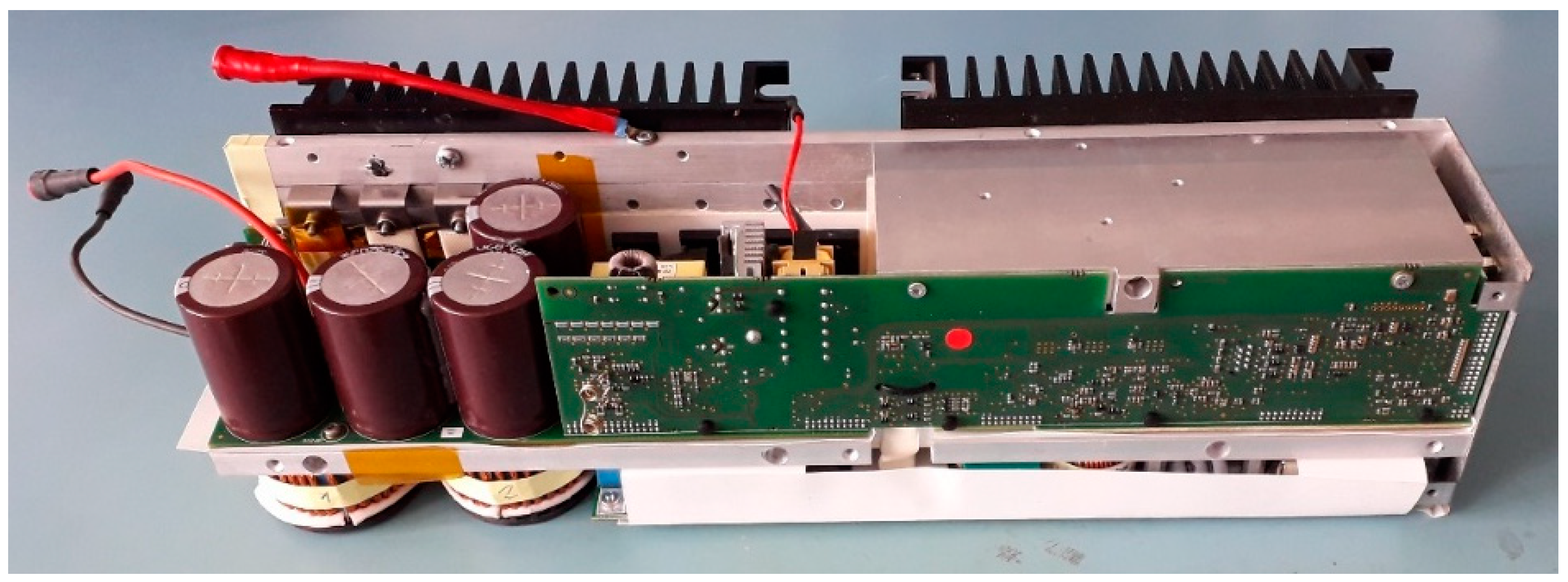
The physical prototype of the PFC converter, whose circuit diagram of the main circuit is shown in
Figure 1, is shown in
Figure 5. It is clear from the parameters listed in
Table 2 that the industrial use of such a system is predestined for the US network. Therefore, GaN and SiC technology transistors (
Table 7), whose blocking voltage is at the level of 600 Vdc to 650 Vdc, will be analyzed.
In the first step, the efficiency and total losses were evaluated, with the original components, and the results will serve as reference values (
Figure 6). The goal of the utilization of progressive semiconductor components should be the increase of the switching frequency together with the increase in efficiency. Therefore, the results given in
Figure 6 use components listed in
Table 2.
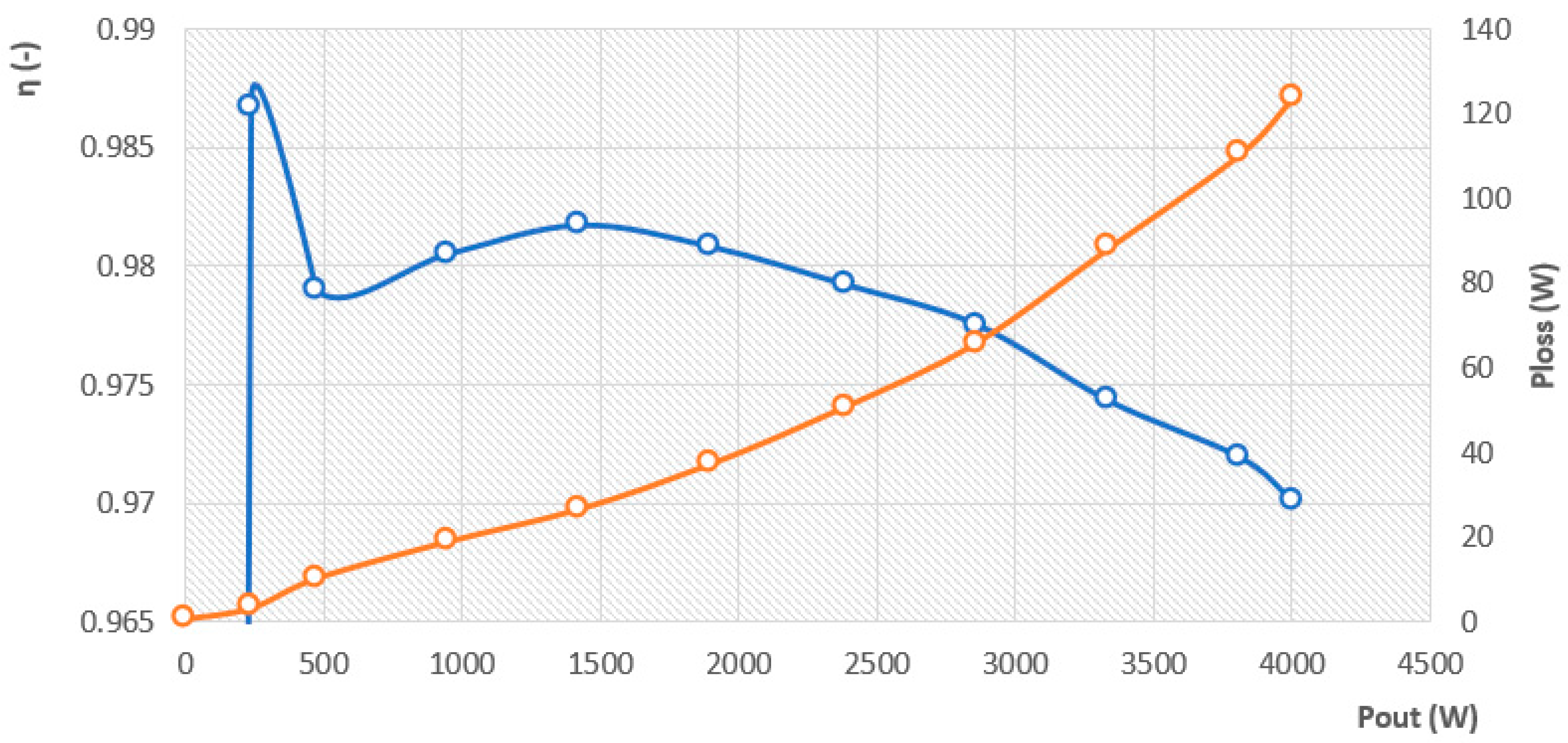
From
Figure 7, it can be seen that the power losses of the circuit shown in
Figure 1 are approximately 100 W. These losses are referred to the input filter stage, rectifier stage, and the PFC circuit (boost converter) itself.
Figure 7 shows the analyzed dependency of power losses on the input common mode filter and the rectifier circuit dependency on input current (i.e., power of the converter as well). It can be seen that sum of those losses represent almost 50% of the total power losses of the proposed PFC converter.
The operation/power losses of the input filter with the rectifier are not dependent on the value of the switching frequency of the PFC. Therefore, the values of the losses on these elements will be constant during further measurements, where the investigated PFC will operate with different switching frequencies. In the following steps, we will calculate the rectifier and filter losses into the total measured losses as these losses are an integral part of the PFC converter.
3. Results
3.1. Results for PFC Efficiency for Original CoolSiC Transistor IMW120R060M1H with Modified Inductor for High-Frequency Operation
The first approach to increasing the switching frequency of the PFC converter under consideration and investigate its efficiency performance was realized with the use of the original SiC transistor (blocking voltage 1200 Vdc). Because high-frequency operation compared to reference value will be applied (within 120 kHz–160 kHz), the replacement of the original alloy inductors was performed, while the inductors shown in
Figure 4 were used. The results are shown in
Figure 8. It can be seen that the efficiency for high-frequency operation dropped within the range of 0.5% if 50% of nominal power is considered.
Evaluation of the power losses related to previous efficiency characteristics (
Figure 8) is shown in
Figure 9. The main part of the losses associated with this efficiency drop are addressed to the switching losses of the transistors and therefore next, the experimental measurements for the selected transistors is shown. The main difference compared to previous results (
Figure 8) is that the transistors with a lower voltage blocking capability have been selected, which should reduce the switching and conduction losses of this semiconductor with the evaluated PFC circuit.
3.2. Optimization of Three-Phase PFC Circuit with the Use of Perspective Transistor Structures
As was previously mentioned, three types of the proposed transistors were selected for evaluation. Individual transistors have similar parameters according to electrical parameters (
Table 8), while they differ technologically.
3.2.1. Results for Cascode GaN Transistor TPH050WS for Switching Frequency 160–200 kHz
The main electrical parameters of this transistor are listed in
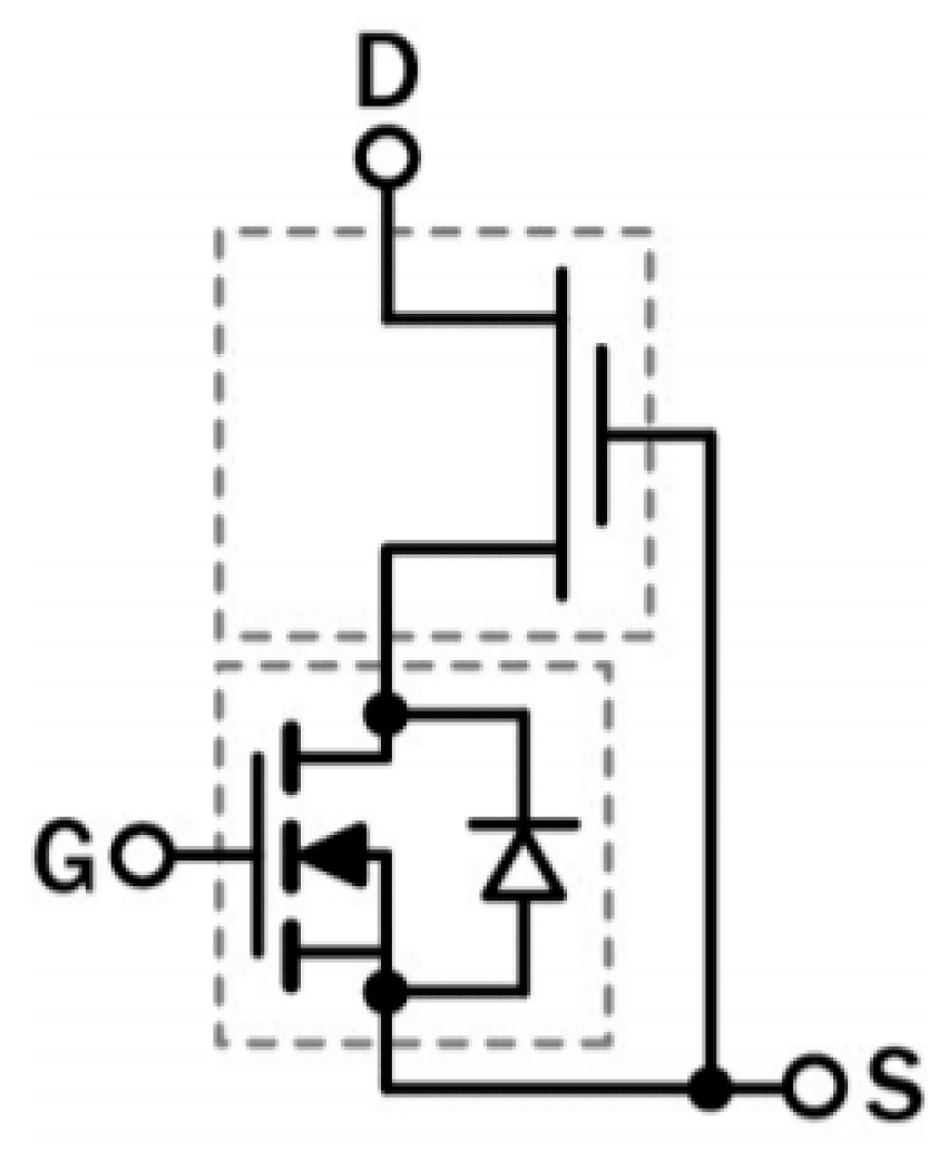
Table 7. As was already mentioned, there is a MOSFET transistor at the input of the cascoded GaN transistor, which controls the power GaN transistor (
Figure 10). The advantage of this cascode connection is the possibility of the utilization of the driving circuit originally used for the reference transistor (CoolSiC IMW120R060M1H), thus no reconfiguration is required as the voltage range of the
UGS is the same as that of the conventional MOSFET. On the other side, the value of the gate resistance does not have a great effect on the turn-on and turn-off speed of the transistor, which is reflected in the transistor’s disadvantage, i.e., a limitation of the switching dynamics of the cascoded GaN transistor.
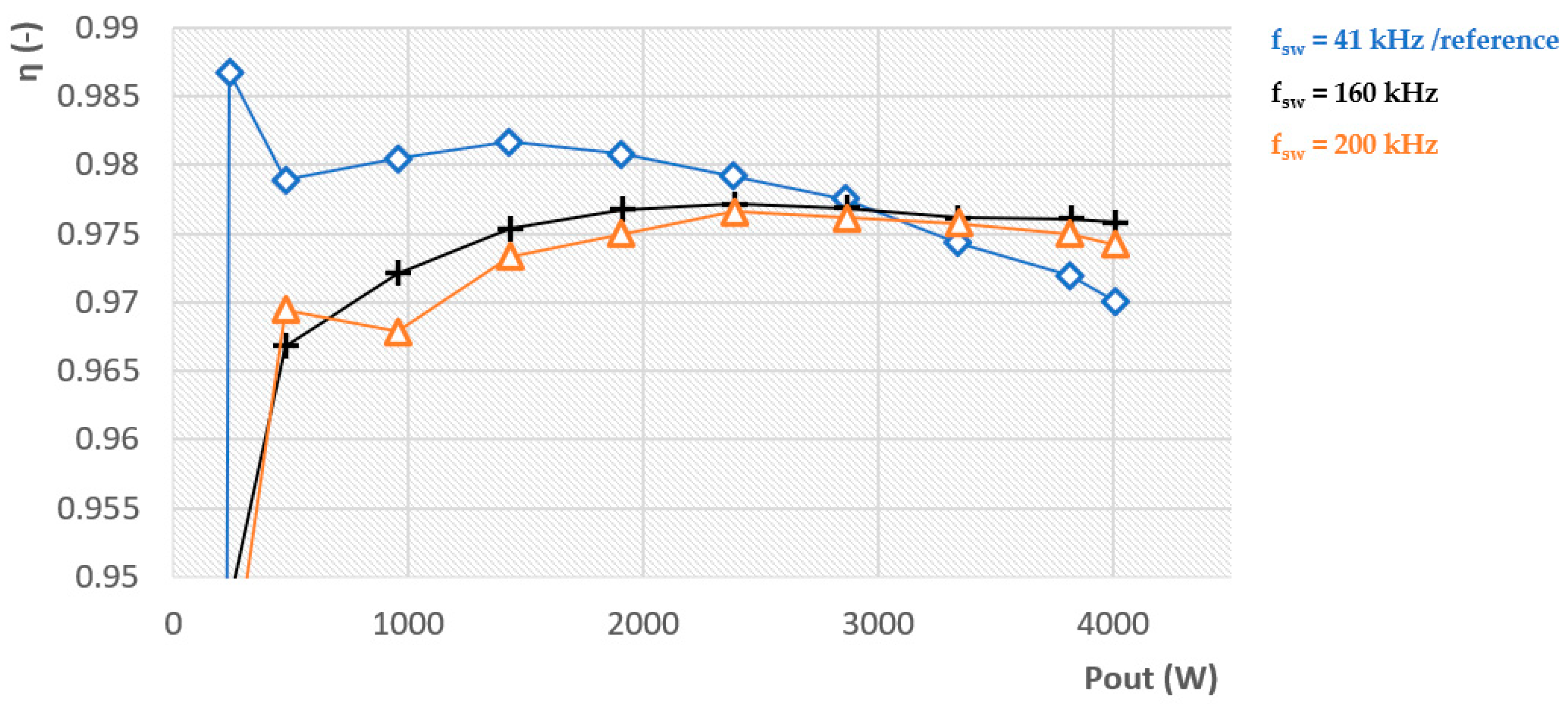
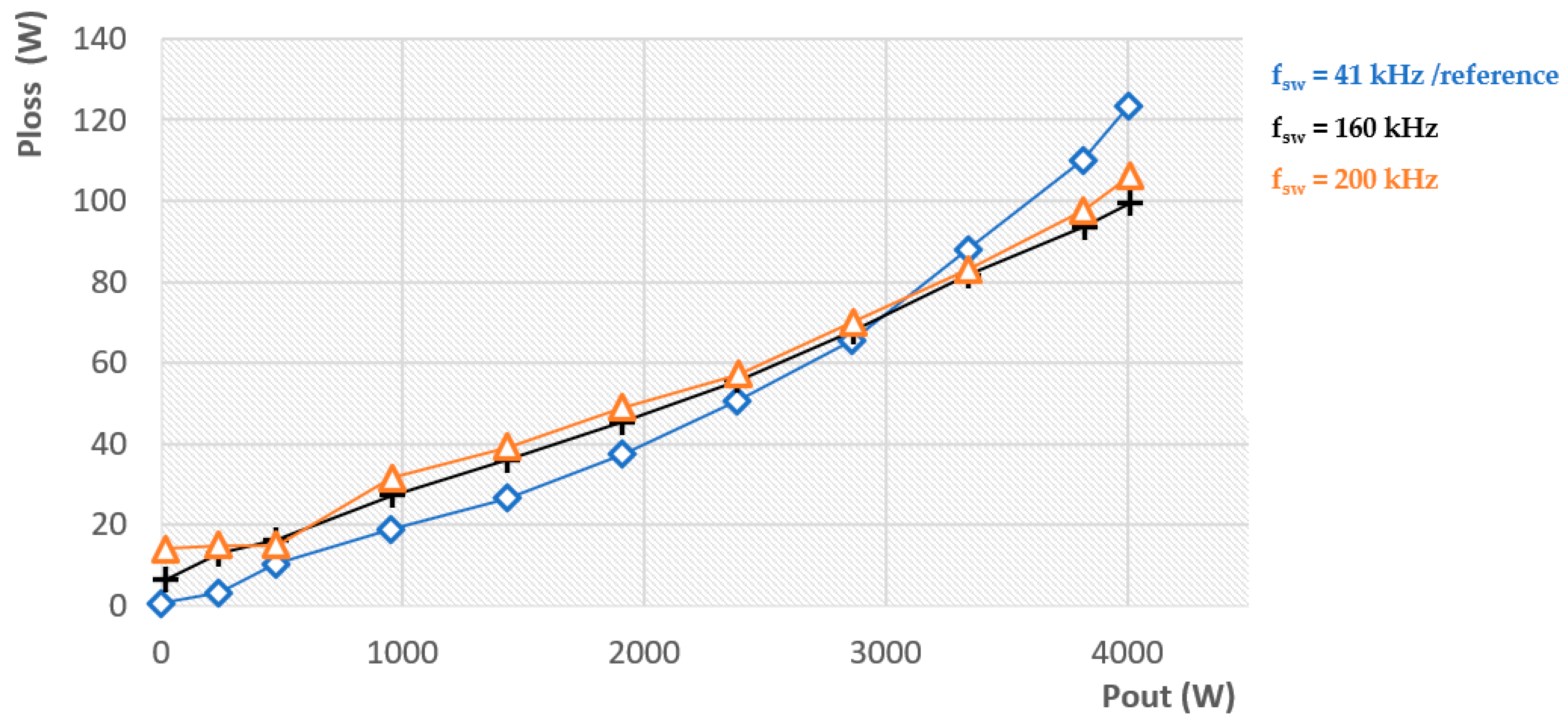
For this type of transistor, the switching frequency was set to 160 kHz as well as 200 kHz. Regarding PFC inductors, ferrite toroidal inductors were used (
Figure 4). The efficiency for the wide output power delivery was evaluated. As can be seen from
Figure 11, the efficiency of the converter has been improved by 0.5% at full power compared to the previous measurement (IMW120R060M1H). Simultaneously, the efficiency characteristic is almost constant from half of the output power compared to the previous measurements. For this situation, where the switching frequency was increased up to 200 kHz (
Figure 11), it can be seen that at nominal output power, the efficiency drop compared to 160 kHz is 0.1% (this is valid almost for the whole power range of the PFC converter). This difference represents approximately 3 W (
Figure 12).
3.2.2. Results for CoolSiC Transistor IMZA65R072M1 for Switching Frequency 200 kHz
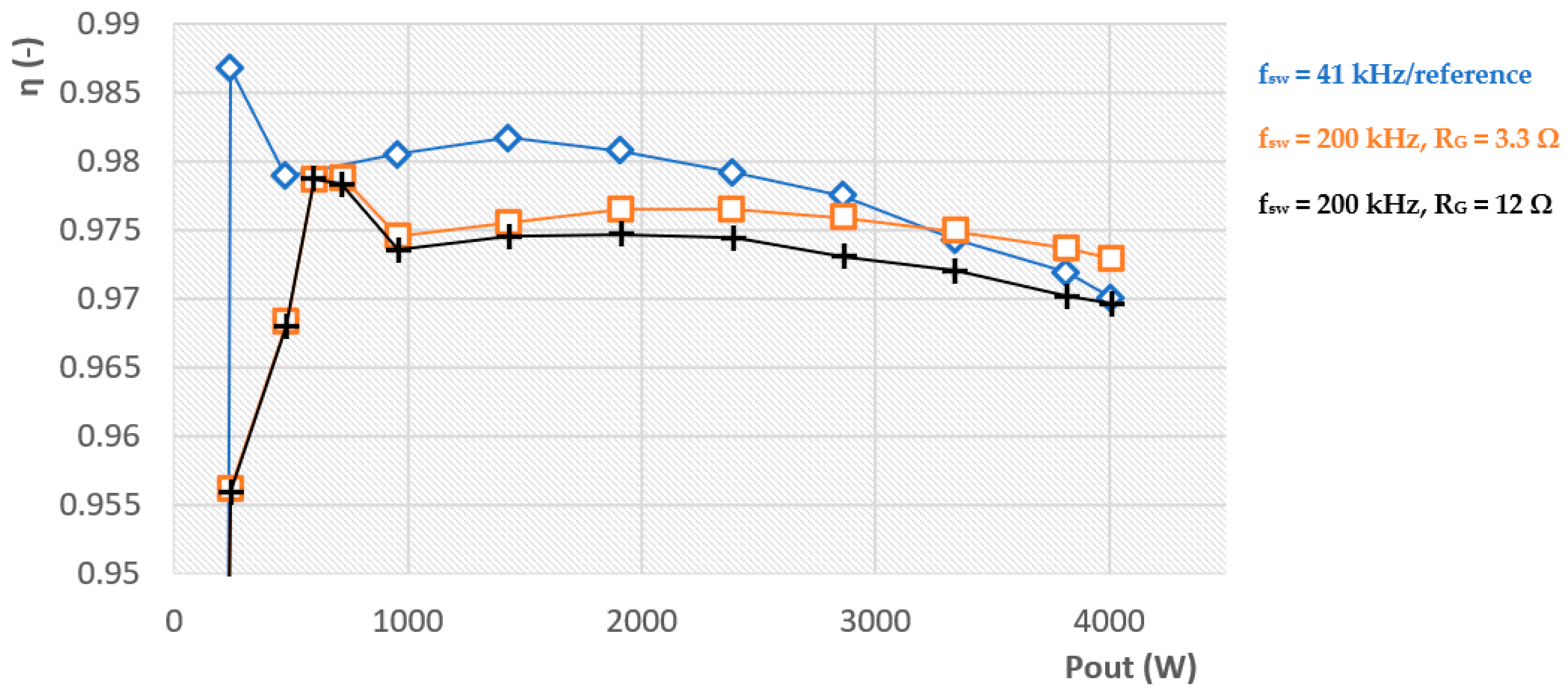
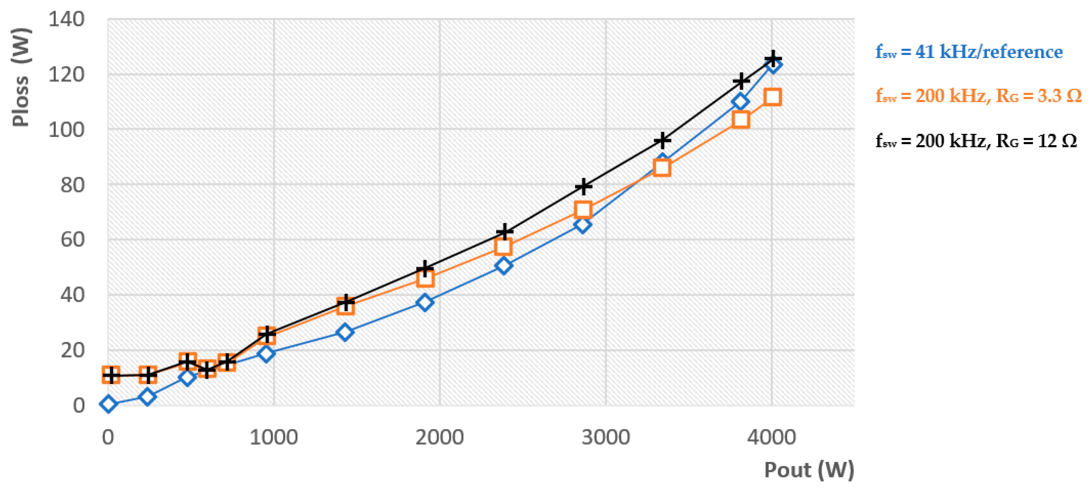
For a more correct comparison of SiC and GaN technologies, it is more appropriate to compare transistors with approximately the same voltage and current parameters. So far, we have tested the original SiC transistor, which has a maximum blocking voltage of
UDS = 1200 V. It would not be adequate to compare this transistor with a 600 V GaN transistor, and therefore a 650 V SiC transistor IMZA65R072M1, the latest generation of CoolSiC from Infineon, was incorporated into the evaluation process. The PFC converter was adapted to the operation at 200 kHz of switching frequency. As opposed to the previous situation, here we were evaluating the effect of the gate resistor on the efficiency performance (i.e., 12 Ω and 3.3 Ω values were tested). It is assumed that the value of the gate resistor will have a significant effect on the switching losses, and thus also on the overall efficiency of the PFC converter (
Figure 13 and
Figure 14).
Comparing the situation with two different values of gate resistors, the difference in efficiency at full power is 0.3% (
Figure 13), which is a difference of 13 W of power losses (
Figure 14). Compared to the reference configuration, in the case of a gate resistor with a value of 3.3 Ω, the efficiency is just 0.3% higher at full power. However, at an output power of around 1.2 kW, this efficiency is 0.65% worse compared to the original configuration.
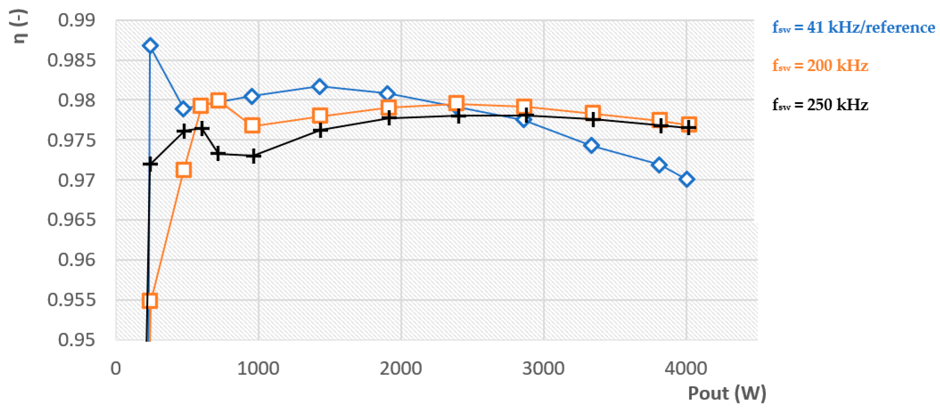
3.2.3. Results for GaN Transistor IGT60R070D1 for Switching Frequency 200–250 kHz
The last type of verified transistor is GaN IGT60R070D1 from Infineon. Unlike conventional MOSFET transistors, this transistor is not controlled by driving voltage, but by driving current. For this reason, modification of the driving circuitry of the PFC converter was required, therefore, additional circuitry was required (
Figure 15) to be added to the original one.
At the instant when the transistor is required to be turned on, 5 V are applied at the OUTH output and a current pulse, which can be in the order of hundreds of milliamperes, is applied to the transistor gate through the low-ohmic resistor R5 (in the order of ohms) and capacitor C9 (in the order of nanofarads). This current pulse opens the transistor, which is opened until capacitor C9 is charged. The current that keeps the transistor opened is in the order of tens of milliamperes (up to 20 mA) and flows through resistor R9, which is in the order of hundreds of ohms. The transistor is turned off by disconnecting 5 V (OUTH) and then grounding resistor R6 via pin OUTL, which applies a negative voltage from capacitor C9 to the gate of the transistor. During the turn-off state, the manufacturer recommends that a negative voltage should be applied continuously to the gate of the transistor. This is provided by the capacitor C9.
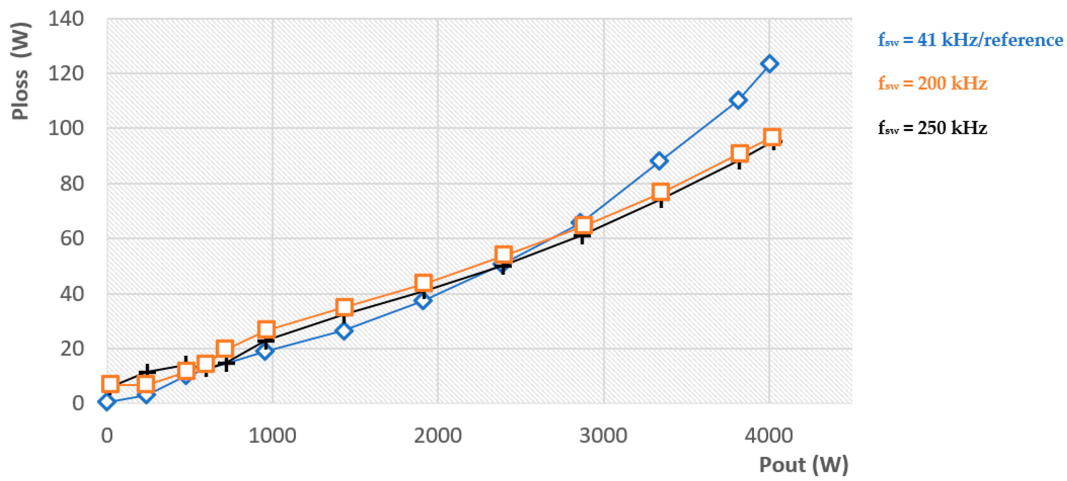
The measurements were performed for two values of switching frequencies, i.e., 200 kHz and 250 kHz. The results of the efficiency characteristic and power loss characteristic in dependency on output power are evaluated in
Figure 16 and
Figure 17.
At 200 kHz and at full power, the efficiency improved by 0.65% compared to the reference values. This represents the best result so far among the evaluated transistor structures. The value of power losses at full power of PFC operation decreased by 28 W, which represents a reduction of almost 2/9 losses compared to the losses of the original configuration, while power density was maintained. Increasing the switching frequency to 250 kHz reduced the efficiency by 0.3% for a output power value of 1 kW, but at full power, the efficiency value was almost identical compared to 200 kHz of switching frequency.
This experiment represents the final step in the circuit optimization of the proposed three-phase PFC converter. Experimental analysis and verification have confirmed that transistors based on GaN technology represent a promising way to increase the quality indicators of power electronic converters.
4. Conclusions
In this paper, the evaluation of the power transistor technology on the efficiency performance of the proposed three-phase PFC converter was given. Because SiC and GaN materials are currently identified as the most widely used transistor technologies, the main focus was given to the determination of their properties within target application. Each material has certain advantages and disadvantages. Specifically, we analyzed SiC and GaN technologies theoretically, analytically and, in the last step, practically by implementing selected transistor types within the main circuit of the PFC converter. From theoretical knowledge, the most advantageous is SiC transistors due to their properties such as switching speed, relatively low switching losses even at higher switching frequencies, relatively low RDS_on, and high voltage blocking capability (1200 V). However, GaN technology offers better properties, especially in terms of switching speed, but currently, they are not at the stage of research and development to be applicable to industrial power supplies. There are few manufacturers in the world that produce reliable GaN transistors capable of operating at voltages greater than 650 V.
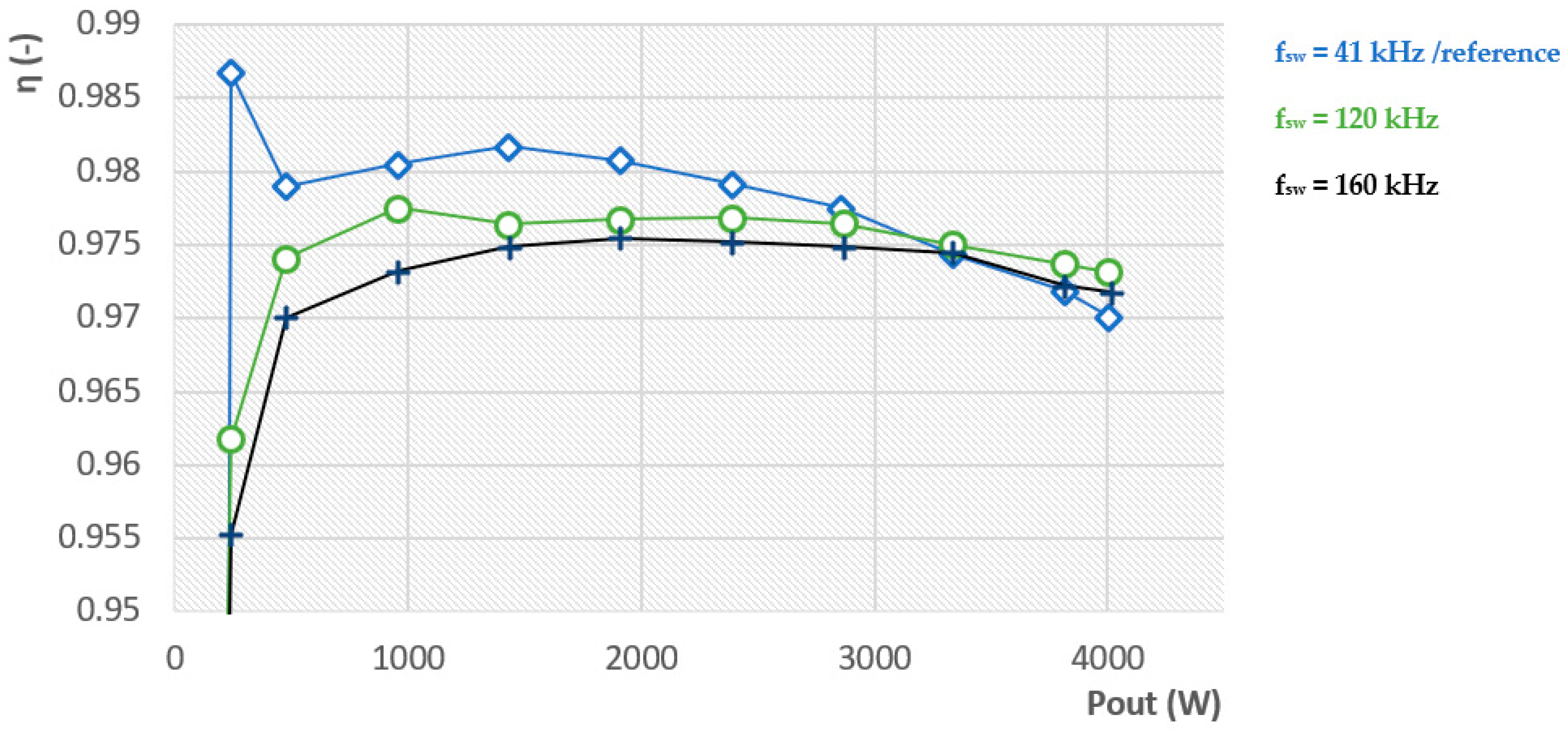
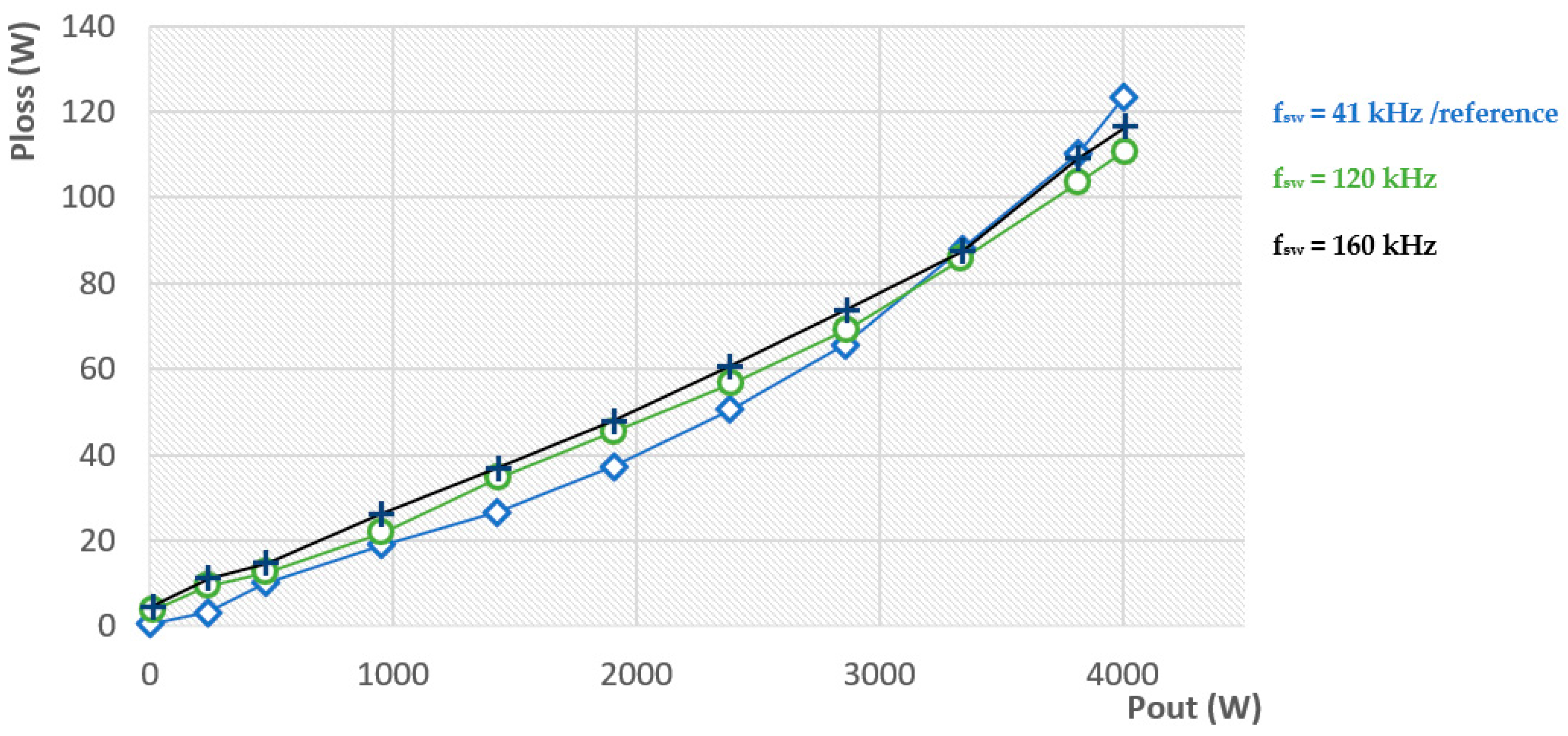
After theoretical analysis of the selected SiC and GaN transistors, the selection of certain types was provided reflecting on currently available devices. Each transistor was evaluated within a certain range of switching frequency. Frequency range was selected dependent on the results of at least two successively measured efficiencies at different switching frequencies. In case the efficiency was worse than the previous one, another type of transistor was tested. The original intention was to optimize the switched power supply operating in three-phase interleaved boost PFC topology. The 600 and 650 V SiC and GaN transistors were specified, which are manufactured by several manufacturers. In the first step, we measured the efficiency and total losses of the original transistor device. These measured values served as a reference, and with increasing switching frequency, we tried to optimize the inverter. In the test, we used four types of transistors, namely, two types of SiC and two types of GaN, where one of the GaNs was in cascade connection with a MOSFET at the gate part. The best efficiency performance was reached for 200 kHz of switching frequency (five times higher value compared to reference), while the efficiency increase compared to reference was 0.7%. This achievement is remarkable if we consider that the efficency is several times higher compared to the original solution. In this way, it is possible to markedly optimize the converter main circuit and thus reduce dimmensions, size, and costs.
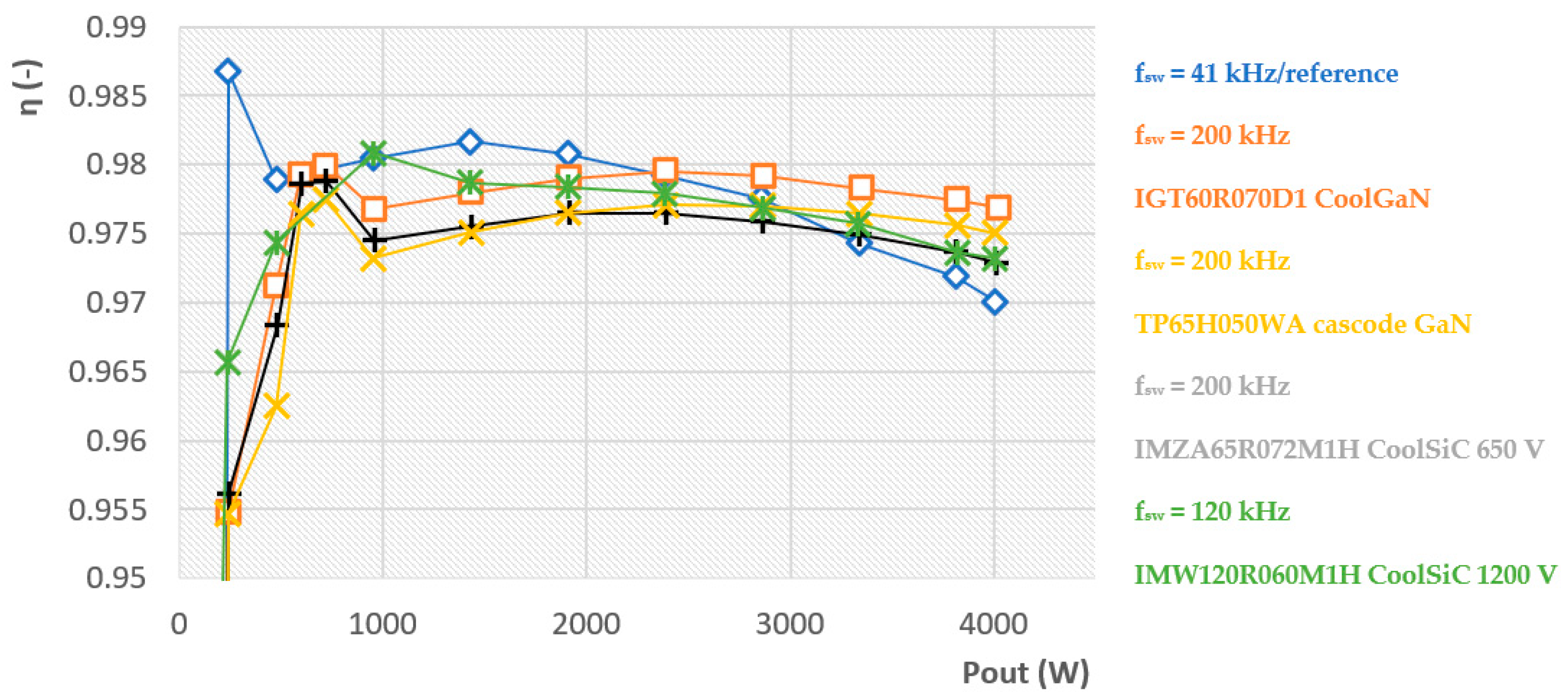
The summary of achieved results is represented in the last figure (
Figure 18). Here, the representation of the achieved results from the measurement is being shown for each of the tested transistors, while only the efficiency characteristic with the best performance is shown. The reference efficiency characteristic remains the original configuration of the PFC converter. If we look at the achieved results, it is clear that GaN transistor technology enables us to maintain very high operational efficiencies, even the switching frequency rises several times compared to original conditions. A very significant parameter, which must be considered if the presented approach is to be practically used, is the evaluation of the transistor parameters. From the presented information in
Table 5, it can be seen that not only technology, but also parasitic capacitances together with dynamic performance (rise and fall times) are influencing switching losses. The output capacitance COSS is influencing the amount of turn-off switching, while CISS is influencing turn-on switching. A good compromise between their values and a very low value of miller capacitance are predicting superior performance if high-frequency, high-efficiency operation is expected. The results given in this paper confirm that in the future, GaN transistors will naturally replace SiC transistors in industrial power supplies. Currently, the biggest disadvantage of available GaN transistors is that they are not usable for 1200 V.
Finally, it must also be mentioned here that the impact of the modifications related to circuit components and operational conditions, i.e., change of transistors, inductors, and switching frequency, does not have significant influence on the performance related to THD and PF. This is confirmed by the measured results, which are given in
Appendix A. It can be seen that there is no visible change or fluctuation of these parameters within the whole power range of evaluated PFC converter.
Author Contributions
Conceptualization by P.S.; methodology, writing—original draft preparation, writing—review and editing, and funding acquisition by M.F.; validation, formal analysis, and investigation by M.P. All authors have read and agreed to the published version of the manuscript.
Funding
This research was funded by national grant agency VEGA 1/0063/21.
Conflicts of Interest
The authors declare no conflict of interest.
Appendix A
In this section, the values for PF and THD of individual phases are given, while the results are listed for the original PFC circuit with alloy inductor and transistor, as well as for optimized and tested solutions.
Table A1.
THD and PF parameters for original transistor SiC IMW120R060M1H and alloy inductor (operating frequency 41 kHz).
Table A1.
THD and PF parameters for original transistor SiC IMW120R060M1H and alloy inductor (operating frequency 41 kHz).
| Pout (W) | THDI1 (%) | THDI2 (%) | THDI3 (%) | PF() |
|---|
| 0 | 0 | 0 | 0 | 0.27 |
| 238.4 | 29.9 | 29.4 | 30.2 | 0.94 |
| 475.3696 | 30.25 | 29.89 | 30.16 | 0.95 |
| 952.6464 | 33.21 | 32.72 | 32.81 | 0.94 |
| 1428.97 | 31.47 | 31.03 | 31.21 | 0.94 |
| 1906.246 | 30.32 | 29.9 | 30.1 | 0.95 |
| 2384.954 | 29.65 | 29.25 | 29.45 | 0.95 |
| 2858.893 | 29.19 | 28.83 | 29.02 | 0.95 |
| 3338.554 | 28.7 | 28.5 | 28.7 | 0.95 |
| 3812.493 | 28.6 | 28.26 | 28.46 | 0.95 |
| 4005.12 | 28.5 | 28.16 | 28.37 | 0.95 |
Table A2.
THD and PF parameters for original transistor SiC IMW120R060M1H and ferrite inductor (operating frequency 120 kHz).
Table A2.
THD and PF parameters for original transistor SiC IMW120R060M1H and ferrite inductor (operating frequency 120 kHz).
| Pout (W) | THDI1 (%) | THDI2 (%) | THDI3 (%) | PF() |
|---|
| 11.44656 | 40 | 40.3 | 40.2 | 0.5106 |
| 238.8868 | 32 | 32 | 32 | 0.9431 |
| 477.2768 | 31.5 | 32 | 32 | 0.9498 |
| 954.0968 | 30.35 | 30.86 | 30.64 | 0.955 |
| 1430.997 | 31.62 | 32 | 32 | 0.9521 |
| 1909.704 | 30.7 | 31.17 | 30.92 | 0.9545 |
| 2389.395 | 30.16 | 30.6 | 30.38 | 0.955 |
| 2865.452 | 29.8 | 30 | 30 | 0.956 |
| 3334.892 | 29.5 | 29.9 | 29.74 | 0.956 |
| 3814.246 | 29.3 | 29.7 | 29.52 | 0.957 |
| 4008.821 | 29.22 | 29.63 | 29.55 | 0.957 |
Table A3.
THD and PF parameters for original transistor GaN TPH65H050WS and ferrite inductor (operating frequency 200 kHz).
Table A3.
THD and PF parameters for original transistor GaN TPH65H050WS and ferrite inductor (operating frequency 200 kHz).
| Pout (W) | THDI1 (%) | THDI2 (%) | THDI3 (%) | PF() |
|---|
| 19.074 | 40.1 | 40.4 | 40.35 | 0.72 |
| 475.8963 | 30.3 | 30.5 | 30.6 | 0.954 |
| 953.72 | 31.7 | 32.2 | 31.9 | 0.946 |
| 1433.441 | 30.7 | 31.2 | 30.9 | 0.9519 |
| 1907.48 | 30.7 | 31.2 | 30.9 | 0.954 |
| 2387.361 | 30.3 | 30.6 | 30.5 | 0.955 |
| 2863.604 | 30 | 30 | 30 | 0.979 |
| 3341.568 | 29.6 | 30 | 29.8 | 0.956 |
| 3816.791 | 29.4 | 29.8 | 29.7 | 0.9568 |
| 4007.545 | 29.3 | 29.78 | 29.5 | 0.9569 |
Table A4.
THD and PF parameters for original transistor SiC IMZA65R072M1 and ferrite inductor (operating frequency 200 kHz).
Table A4.
THD and PF parameters for original transistor SiC IMZA65R072M1 and ferrite inductor (operating frequency 200 kHz).
| Pout (W) | THDI1 (%) | THDI2 (%) | THDI3 (%) | PF() |
|---|
| 19.5529 | 43.712 | 43.109 | 43.354 | 0.704 |
| 481.6488 | 32.917 | 33.902 | 34.313 | 0.9405 |
| 599.915 | 32.21 | 32.986 | 33.192 | 0.9438 |
| 720.0888 | 28.991 | 29.613 | 30.042 | 0.9516 |
| 958.7471 | 32.16 | 32.748 | 33.806 | 0.9411 |
| 1432.994 | 31.188 | 31.772 | 32.005 | 0.9452 |
| 1914.156 | 29.61 | 30.205 | 30.57 | 0.9475 |
| 2387.361 | 28.6 | 29.222 | 28.937 | 0.9498 |
| 2865.812 | 28.074 | 28.686 | 28.518 | 0.9504 |
| 3342.354 | 27.47 | 27.959 | 27.806 | 0.9503 |
| 3816.552 | 26.723 | 27.338 | 27.142 | 0.9494 |
| 4008.513 | 26.477 | 27.218 | 26.834 | 0.9498 |
Table A5.
THD and PF parameters for original transistor GaN IGT60R070D1 and ferrite inductor (operating frequency 200 kHz).
Table A5.
THD and PF parameters for original transistor GaN IGT60R070D1 and ferrite inductor (operating frequency 200 kHz).
| Pout (W) | THDI1 (%) | THDI2 (%) | THDI3 (%) | PF() |
|---|
| 19.076 | 45.59 | 48.108 | 44.166 | 0.6441 |
| 478.8277 | 32.504 | 32.993 | 33.73 | 0.9411 |
| 598.9864 | 32.359 | 33.396 | 32.823 | 0.9446 |
| 720.1492 | 29.573 | 31.032 | 30.445 | 0.9508 |
| 958.77 | 32.37 | 33.052 | 33.851 | 0.9415 |
| 1434.283 | 31.4 | 31.906 | 31.875 | 0.9465 |
| 1915.918 | 29.863 | 30.31 | 30.47 | 0.9495 |
| 2391.927 | 29.498 | 30.606 | 29.188 | 0.9512 |
| 2869.05 | 28.636 | 28.911 | 28.911 | 0.9511 |
| 3349.972 | 27.564 | 28.423 | 28.385 | 0.9504 |
| 4025.999 | 27.015 | 27.595 | 27.293 | 0.9505 |
References
- Kolar, J.W.; Friedli, T. The essence of three-phase PFC rectifier systems. In Proceedings of the 2011 IEEE 33rd International Telecommunications Energy Conference (INTELEC), Amsterdam, The Netherlands, 9–13 October 2011; pp. 1–27. [Google Scholar] [CrossRef]
- Azazi, H.Z.; Mahmoud, S.A.; Shokralla, S.S. Review of Passive and Active Circuits for Power Factor Correction in Single Phase, Low Power AC-DC Converters; Menoufiya University: Shebin El-Kom, Egypt, 2010. [Google Scholar]
- Mohan, N.; Undeland, T.; Robbins, W. Power Electronics; John Whiley and Sons: Hoboken, NJ, USA, 1995; ISBN 0-471-58408-8. [Google Scholar]
- Liu, B.; Ren, R.; Jones, E.; Wang, F.; Costinett, D.; Zhang, Z. A compensation scheme to reduce input current distortion in a GaN based 450 kHz three-phase Vienna type PFC. In Proceedings of the 2016 IEEE Energy Conversion Congress and Exposition (ECCE), Milwaukee, WI, USA, 18–22 September 2016; pp. 1–7. [Google Scholar] [CrossRef]
- Zhu, H.; Li, B.; Wang, K.; Yang, X. Common-Mode EMI Modeling and Analysis for GaN-Based Full-Bridge CRM PFC under Unipolar PWM Scheme. In Proceedings of the 2020 IEEE Workshop on Wide Bandgap Power Devices and Applications in Asia (WiPDA Asia), Virtual Conference, 23–25 September 2020; pp. 1–5. [Google Scholar] [CrossRef]
- Do, N.-N.; Huang, B.-S.; Phan, N.-T.; Nguyen, T.-T.; Wu, J.-H.; Liu, Y.-C.; Chiu, H.-J. Design and Implementation of a Control Method for GaN-Based Totem-Pole Boost-Type PFC Rectifier in Energy Storage Systems. Energies 2020, 13, 6297. [Google Scholar] [CrossRef]
- Lechat, S.S. Voltage Oriented Control of Three-Phase Boost PWM Converters. Master’s Thesis, Chalmers University of Technology, Goteborg, Sweden, 2010. [Google Scholar]
- Microsemi, P.P.G. Gallium Nitride (GaN) versus Silicon Carbide (SiC) in the High Frequency (RF) and Power Switching Applications. Available online: https://www.arrow.com/en/research-and-events/articles/silicon-carbide-and-gallium-nitride-compared (accessed on 14 May 2021).
- Kachi, T. Current status of GaN power devices. IEICE Electron. Express 2013, 10, 20132005. [Google Scholar] [CrossRef] [Green Version]
- Kolar, J.W.; Muhlethaler, J. The Essence of Three-Phase PFC Rectifier Systems; Swiss Federal Institute of Technology (ETH) Zurich, Power Electronic systems Laboratory: Zürich, Switzerland, 2011. [Google Scholar]
- Huang, X.; Chen, W. An Improved Calculation Method of High-Frequency Winding Losses for Gapped Inductors; Fujian University of Technology: Fuzhou, China, 2017. [Google Scholar]
- Wong, F.K.; Eng, B.; Phil, M. High Frequency Transformer for Switching Mode Power Supplies; School of Microelectronic Engineering, Griffith University: Brisbane, Australia, 2004. [Google Scholar]
- Zeng, F.; An, J.X.; Zhou, G.; Li, W.; Wang, G.; Duan, T.; Jiang, L.; Yu, G. A Comprehensive Review of Recent Progress on GaN High Electron Mobility Transistors: Devices, Fabrication and Reliability; Southern University of Science and Technology: Shenzhen, China, 2018. [Google Scholar]
- Schonberger, J. Space Vector Control of a Three-Phase Rectifier Using PLECS. Available online: http://www.plexim.com/sites/default/files/plecs_svm. pdf (accessed on 22 March 2016).
- Jimenez, H.O. AC Resistance Evaluation of Foil, Round and Litz Conductors in Magnetic Components. Master’s Thesis, Chalmers University of Technology, Goteborg, Sweden, 2013. [Google Scholar]
- Sullivan, C.R.; Zhang, R.Y. Simplified Design Method for Litz Wire; Thayer School of Engineering at Dartmouth, M.I.T. Cambridge: Cambridge, MA, USA, 2014. [Google Scholar]
- Tourkhani, F.; Viarouge, P. Accurate Analytical Model of Winding Losses in Round Litz Wire Windings. IEEE Trans. Magn. 2001, 37, 538–543. [Google Scholar] [CrossRef]
- McLyman, C.W.T. Transformer and Inductor Design Gandbook; CRC Press: Boca Raton, FL, USA, 2017; ISBN 9781439836880. [Google Scholar]
Figure 1.
Main circuit of the three-phase power factor correction (PFC) interleaved converter.
Figure 1.
Main circuit of the three-phase power factor correction (PFC) interleaved converter.
Figure 2.
Experimental test-stand for PFC optimization.
Figure 2.
Experimental test-stand for PFC optimization.
Figure 3.
Block diagram of the experimental measurements.
Figure 3.
Block diagram of the experimental measurements.
Figure 4.
Ferrite toroidal inductor with distributed airgap optimized for high-frequency evaluation of selected transistor structures within considered PFC circuit.
Figure 4.
Ferrite toroidal inductor with distributed airgap optimized for high-frequency evaluation of selected transistor structures within considered PFC circuit.
Figure 5.
Physical prototype of three-phase PFC converter used for optimization purposes and evaluation.
Figure 5.
Physical prototype of three-phase PFC converter used for optimization purposes and evaluation.
Figure 6.
Efficiency characteristic of analyzed non-optimized PFC converter and power loss dependency on the output power of converter.
Figure 6.
Efficiency characteristic of analyzed non-optimized PFC converter and power loss dependency on the output power of converter.
Figure 7.
Efficiency characteristic of analyzed non-optimized PFC converter and power loss dependency on the output power of converter.
Figure 7.
Efficiency characteristic of analyzed non-optimized PFC converter and power loss dependency on the output power of converter.
Figure 8.
Efficiency characteristic of analyzed non-optimized PFC converter in dependency on the output power and switching frequency (equipped with IMW120R060M1H SiC transistor).
Figure 8.
Efficiency characteristic of analyzed non-optimized PFC converter in dependency on the output power and switching frequency (equipped with IMW120R060M1H SiC transistor).
Figure 9.
Total power losses of analyzed non-optimized PFC converter in dependency on the output power and switching frequency.
Figure 9.
Total power losses of analyzed non-optimized PFC converter in dependency on the output power and switching frequency.
Figure 10.
GaN transistor in cascode connection with MOSFET transistor.
Figure 10.
GaN transistor in cascode connection with MOSFET transistor.
Figure 11.
Efficiency characteristic of PFC converter equipped with TP65H050WS GaN transistor in dependency on the output power and switching frequency (blue line—referenced non-optimized solution).
Figure 11.
Efficiency characteristic of PFC converter equipped with TP65H050WS GaN transistor in dependency on the output power and switching frequency (blue line—referenced non-optimized solution).
Figure 12.
Power losses of PFC converter equipped with TP65H050WS GaN transistor in dependency on the output power and switching frequency (blue line—referenced non-optimized solution).
Figure 12.
Power losses of PFC converter equipped with TP65H050WS GaN transistor in dependency on the output power and switching frequency (blue line—referenced non-optimized solution).
Figure 13.
Efficiency characteristic of PFC converter equipped with IMZA65R072M1 SiC transistor in dependency on the output power and switching frequency (blue line—referenced non-optimized solution).
Figure 13.
Efficiency characteristic of PFC converter equipped with IMZA65R072M1 SiC transistor in dependency on the output power and switching frequency (blue line—referenced non-optimized solution).
Figure 14.
Power losses of PFC converter equipped with IMZA65R072M1 SiC transistor in dependency on the output power and switching frequency (blue line—referenced non-optimized solution).
Figure 14.
Power losses of PFC converter equipped with IMZA65R072M1 SiC transistor in dependency on the output power and switching frequency (blue line—referenced non-optimized solution).
Figure 15.
Principal schematic of the driving circuit for transistor TPH050WS.
Figure 15.
Principal schematic of the driving circuit for transistor TPH050WS.
Figure 16.
Efficiency characteristic of PFC converter equipped with IGT60R070D1 GaN transistor in dependency on the output power and switching frequency (blue line—referenced non-optimized solution).
Figure 16.
Efficiency characteristic of PFC converter equipped with IGT60R070D1 GaN transistor in dependency on the output power and switching frequency (blue line—referenced non-optimized solution).
Figure 17.
Power losses of PFC converter equipped with IGT60R070D1 GaN transistor in dependency on the output power and switching frequency (blue line—referenced non-optimized solution).
Figure 17.
Power losses of PFC converter equipped with IGT60R070D1 GaN transistor in dependency on the output power and switching frequency (blue line—referenced non-optimized solution).
Figure 18.
Final comparison of received results.
Figure 18.
Final comparison of received results.
Table 1.
Designation type of used laboratory equipment.
Table 1.
Designation type of used laboratory equipment.
| Laboratory Equipment | Part Number |
|---|
| Power supply | California Instruments CSW5550 |
| Electronic load | Hocherl & Hackl ZS7080 |
| Input power meter | HIOKI PW3337/YOKOGAWA WT330 |
| Output ammeter | Fluke 45 |
| Output voltmeter | Agilent 34401A |
| Osciloscope | MDO3014 |
Table 2.
Main input-to-output operational parameters of non-optimized three-phase PFC circuit and circuit components specification.
Table 2.
Main input-to-output operational parameters of non-optimized three-phase PFC circuit and circuit components specification.
| Parameter | Value |
|---|
| Input Voltage | 210 Vac (3L-PE) |
| Output Voltage | 480 Vdc |
| Output Power | 4 kW |
| Switching frequency | 41 kHz 1 |
| Cooling type | Air-cooled aluminum plate |
| Efficiency | 97% at nominal power |
| Circuit Component | Type |
| Power transistor (T1, T2) | IMW120R060M1H |
| Power diode (D1, D2) | C4D10120D |
| Boost inductor | Alloy type inductor |
| AC side diode rectifier | 36MT120 |
Table 3.
Design parameters of the PFC inductors for high-frequency operation.
Table 3.
Design parameters of the PFC inductors for high-frequency operation.
| Property | Value |
|---|
| Type of the core (-) | Ferrite N87 R50/30/20 |
| Value of inductance (µH) | 248 |
| Maximal current (A) | 11.5 |
| Airgap (mm) | 4 × 0.4 |
| Nr. Of turns (-) | 42 |
| Number of winding layers (-) | 1 |
| Type of wire (-) | 2 × 20 × 0.2 litz |
Table 4.
Comparisons of the material properties for power transistor fabrication.
Table 4.
Comparisons of the material properties for power transistor fabrication.
| Material Property | Si | SiC | GaN |
|---|
| Bandgap (eV) | 1.1 | 3.2 | 3.4 |
| Electric field (106 V/cm) | 0.3 | 3 | 3.5 |
| Electron mobility (cm2/Vs) | 1450 | 900 | 2000 |
| Saturation electron velocity (106 cm/s) | 10 | 22 | 25 |
| Thermal conductivity (W/cm2K) | 1.5 | 5 | 1.3 |
| Max. operation temperature (°C) | 150 | 1000 | 900 |
Table 5.
Basic parameters of GaN and SiC selected power transistors for power loss calculation.
Table 5.
Basic parameters of GaN and SiC selected power transistors for power loss calculation.
| Parameter/Type | IMZA65R072M1H (SiC) | IGT60E070D1 (GaN) |
|---|
| UDS | 650 V | 600 V |
| RDS_on | 72 mΩ | 70 mΩ |
UGS_max
IGS_max | −5 do + 23 V
- | -
20 mA |
| IGS_pulz | - | 2000 mA
@ tpulse = 50 ns,
f = 100 kHz |
| IDS (DC) | 28 A @ 25 °C,
18 A @ 100 °C | 31 A @ 25 °C
20 A @ 100 °C |
| IDS (Pulse) | 69 A @ Tj,max | 60 A @ 25 °C |
| Ptot(max) | 96 W @ 25 °C | 125 W @ 25 °C |
| CISS | 750 pF @ 500 V | 400 pF @ 500 V |
| COSS | 90 pF @ 500 V | 70 pF @ 500 V |
| CRSS | 9 pF @ 500 V | 0.4 pF @ 500 V |
| QG max | 22 nC @ 400 V | 5.8 nC @400 V |
| tr | 15 ns | 10 ns |
| tf | 13 ns | 9 ns |
Table 6.
Comparison of individual parts of power losses for selected transistors.
Table 6.
Comparison of individual parts of power losses for selected transistors.
| Parameter/Type | IMZA65R072M1H (SiC) | IGT60E070D1 (GaN) |
|---|
| Ploss_t(on) [W] | 5.56 | 3.71 |
| Ploss_t(off) [W] | 7.46 | 5.16 |
| Ploss_sw [W] | 13.02 | 8.87 |
| Ploss_cond [W] | 2.42 | 2.35 |
| Ploss_cap [W] | 2.15 | 1.67 |
| Ploss_total [W] | 17.58 | 12.89 |
Table 7.
Types of GaN and SiC transistors which have undergone experimental testing.
Table 7.
Types of GaN and SiC transistors which have undergone experimental testing.
| Type of Transistor | Manufacturer | Technology | (UDS_max) | Package |
|---|
| TP65H050WS | Transphorm | Cascode GaN | 650 V | TO247-3 |
| IMZA65R072M1H | Infineon | CoolSiC | 650 V | TO247-4-3 |
| IGT60R070D1 | Infineon | CoolGaN | 600 V | PG-HSOF-8-3 |
Table 8.
Main electrical parameters of selected transistors.
Table 8.
Main electrical parameters of selected transistors.
| Parameter/Transistor | TP65H050WS | IMZA65R072M1H | IGT60R070D1 |
|---|
| UDS | 650 V | 650 V | 600 V |
| RDS_on | 60 mΩ | 72 mΩ | 70 mΩ |
UGS_max
IGS_max | −20 do + 20 V
- | −5 do + 23 V
- | -
20 mA |
| IGS_pulse | - | - | 2000 mA
@ tpulse = 50 ns,
f = 100 kHz |
| IDS - DC | 36 A @ 25 °C, 25 A @ 100 °C | 28 A @ 25 °C
18 A @ 100 °C | 31 A @ 25 °C, 20 A @ 100 °C |
| IDS - pulse | 150 A @ tpulz = 10 µs | 69 A @ Tj,max | 60 A @ 25 °C |
| Ptot - max | - | 96 W @ 25 °C | 125 W @ 25 °C |
| CISS | 1000 pF @500 V | 750 pF @ 500 V | 400 pF @ 500 V |
| COSS | 12 pF @ 500 V | 90 pF @ 500 V | 70 pF @ 500 V |
| CRSS | 7 pF @ 500 V | 9 pF @ 500 V | 0.4 pF @ 500 V |
| QG max | 24 nC @ 400 V | 22 nC @ 400 V | 5.8 nC @400 V |
| Publisher’s Note: MDPI stays neutral with regard to jurisdictional claims in published maps and institutional affiliations. |
© 2021 by the authors. Licensee MDPI, Basel, Switzerland. This article is an open access article distributed under the terms and conditions of the Creative Commons Attribution (CC BY) license (https://creativecommons.org/licenses/by/4.0/).


