Article

A Pipeline-TDC-Based CMOS Temperature Sensor with a 48 fJ·K2 Resolution FoM

National and Local Joint Engineering Laboratory of RF Integration and Micro-Assembly Technology, College of Electronic and Optical Engineering & College of Microelectronics, Nanjing University of Posts and Telecommunications, Nanjing 210023, China
*
Author to whom correspondence should be addressed.
Electronics 2021, 10(13), 1542; https://doi.org/10.3390/electronics10131542
Submission received: 1 June 2021 / Revised: 17 June 2021 / Accepted: 24 June 2021 / Published: 25 June 2021

Abstract

:
An energy-efficient temperature sensor is important for temperature monitoring in Biomedical Internet-of-things (BIoT) applications. This article presents a time-domain temperature sensor with a pipeline time-to-digital converter (TDC). A programmable-gain time amplifier (PGTA) with high linearity and wide linear range is proposed to improve the resolution of the sensor and to reduce the chip area. The conversion time of the sensor is reduced by the fast TDC that only needs ~26 ns/conversion, which means the sensor is suitable for BIoT applications that commonly use duty cycling mode. Fabricated in a 40 nm standard CMOS technology, the sensor consumes 7.6 μA at a 0.6 V supply and achieves a resolution of 90 mK and a sensitivity of 0.62%/°C in a 1.3 μs conversion time. This translates into a resolution figure-of-merit of 48 fJ·K2. The sensor achieves an inaccuracy of 0.39 °C from −20 °C to 80 °C after two-point calibration. Duty cycling the sensor results in an even lower average power: ~18.6 nW at 10 conversions/s.

1. Introduction

A smart temperature sensor is one of the most commonly desired parts in Internet of Things (IoT) devices to monitor either environment or chip conditions [1]. The temperature sensors that have high energy efficiency and are of low cost can be used in many BIoT applications, for example, the preservation and transport of vaccines, medicines, blood samples, and other medical samples that should be placed in a certain temperature range. Duty cycling is a commonly used mode in a BIoT system, which requires the sensors switching between the on and off states to extend the batter life. As shown in 
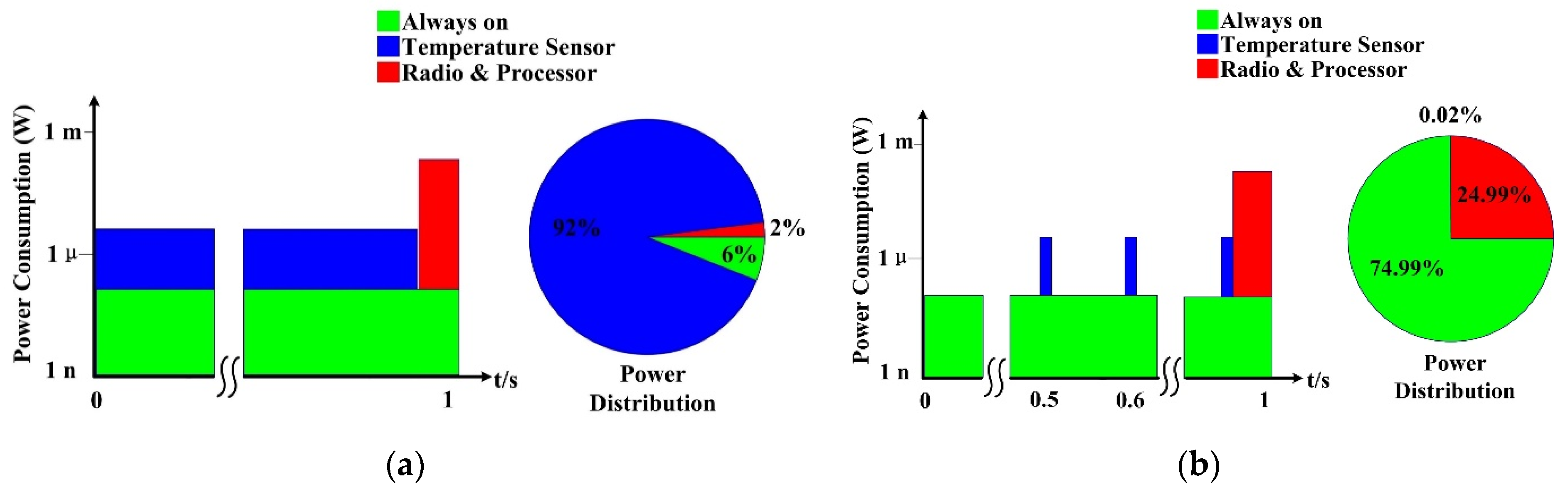
Figure 1a, the temperature sensor consumes 4.6 μW and it is always on just like other always-on modules that consume 300 nW. The processor and radio frequency module are activated to process and transmit data, which takes 1 ms at a 100 μW normalized power consumption. The temperature sensor consumes 92% of the total power consumption that is 5 μW, which is unacceptable for most BIoT applications. When the temperature sensor works on a duty-cycling mode, it is activated every 100 ms to take a measurement which takes only 1.3 μs consuming a 31 nA leakage current. The temperature sensor consumes only 0.02% of the total power consumption that is reduced to 400 nW. Thus, the conversion time of a temperature sensor should be as short as possible in order to reduce the effective power contribution on a BIoT system. According to
P = C F V 2
where C is the equivalent capacitor, F is the frequency and V is the supply voltage. Reducing the supply voltage is beneficial to further reduce the power consumption. It means that a temperature sensor that works at a near-threshold-voltage supply has an advantage over the one that works at a normal-voltage supply. In addition, a temperature sensor should be compact and compatible with the CMOS process to reduce the cost.
Previous researches proposed various kinds of temperature sensors with different principles. A traditional voltage domain temperature sensor used BJT to generate proportional to absolute temperature (PTAT) voltages and then converted the voltages into a digital temperature reading with a ΔΣ-Analog-to-Digital Converter (ADC) [2]. It is both energy and area consuming to implement a high-resolution ΔΣ-ADC. The higher working voltage (>1 V) required by BJT is not suitable for the BIoT applications. In [3], a resistive-type temperature sensor achieved a high sensitivity up to 1.09%/°C, but it is not easy to be integrated, so it is not suitable for the BIoT applications. An alternative method is to use frequency or phase information to express temperature information. In [4], researchers used two Voltage-Controlled Oscillators (VCOs) with different temperature-sensitive characteristics to convert the temperature change into a frequency change, and thus into a temperature reading by counter. With two oscillators operating at dozens of MHz frequency, they achieved a short conversion time of 6.5~22 μs, but this resulted in a high power consumption of about 154 μW. To solve the problem of power consumption, two MOSFETs operating in a sub-threshold region are used to sense the variation of temperature and generated two reference currents. Then, the ratio of currents are transformed into an output frequency difference between the two VCOs working in dozens of kHz frequency. The counter counts the frequency difference and outputs a temperature reading. However, this low-frequency method resulted in a longer conversion times of 59 ms [5]. Resistance-based temperature sensors are usually implemented by RC filters [6], which output temperature-related phase signal. This kind of temperature sensors can achieve high resolutions, but they are not quite suitable for BIoT applications due to high power consumption and long conversion time. In addition, researchers also expressed temperature information using time domain signal. In Ref. [7], a delay line was designed to generate temperature-dependent time signal, and a cyclic time-to-digital convertor (TDC) outputs temperature reading. In [8], a delay line was reused to sense the temperature in a sensing module and measure the PTAT pulse in a TDC. Time domain temperature sensors achieve better power consumption and smaller area.
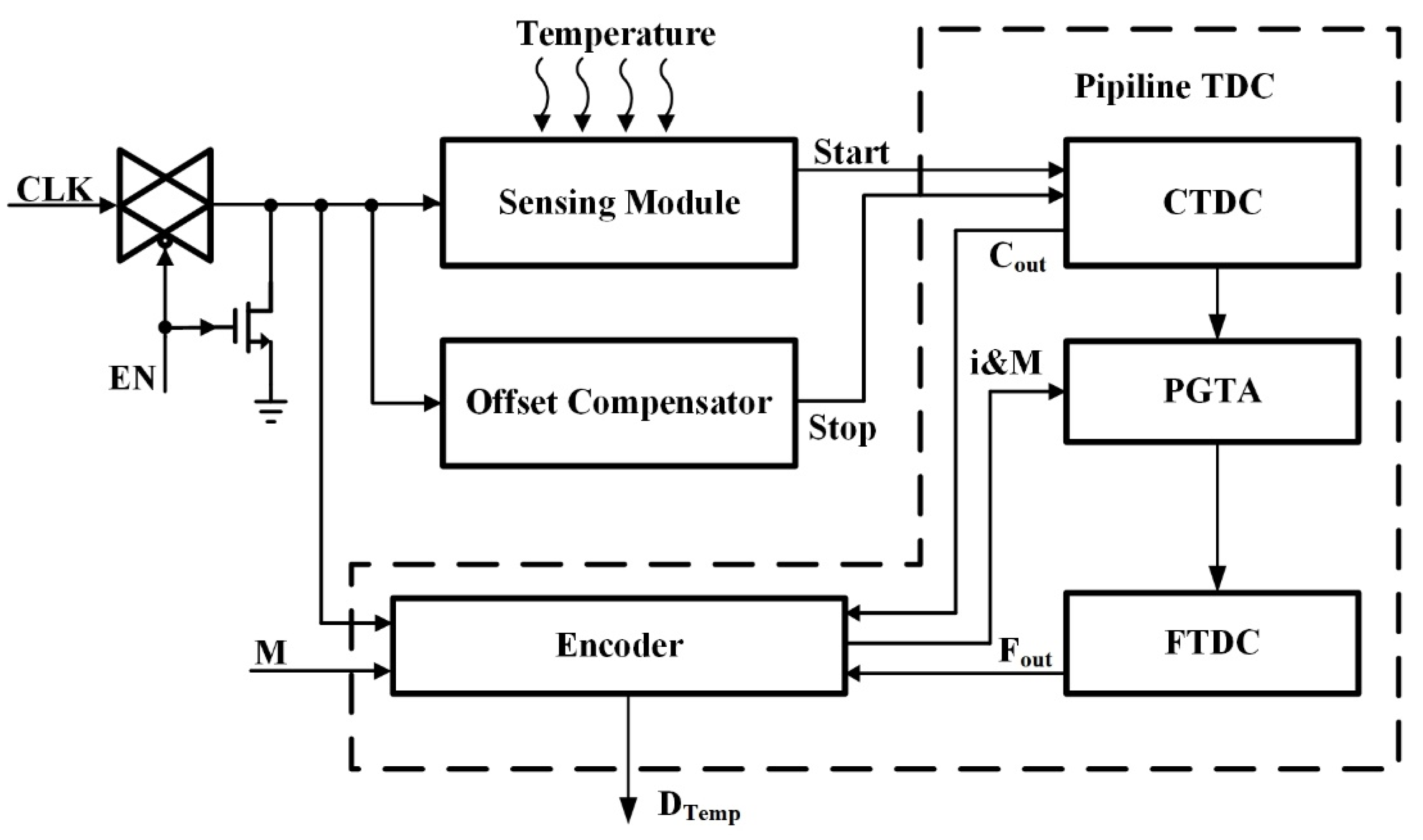
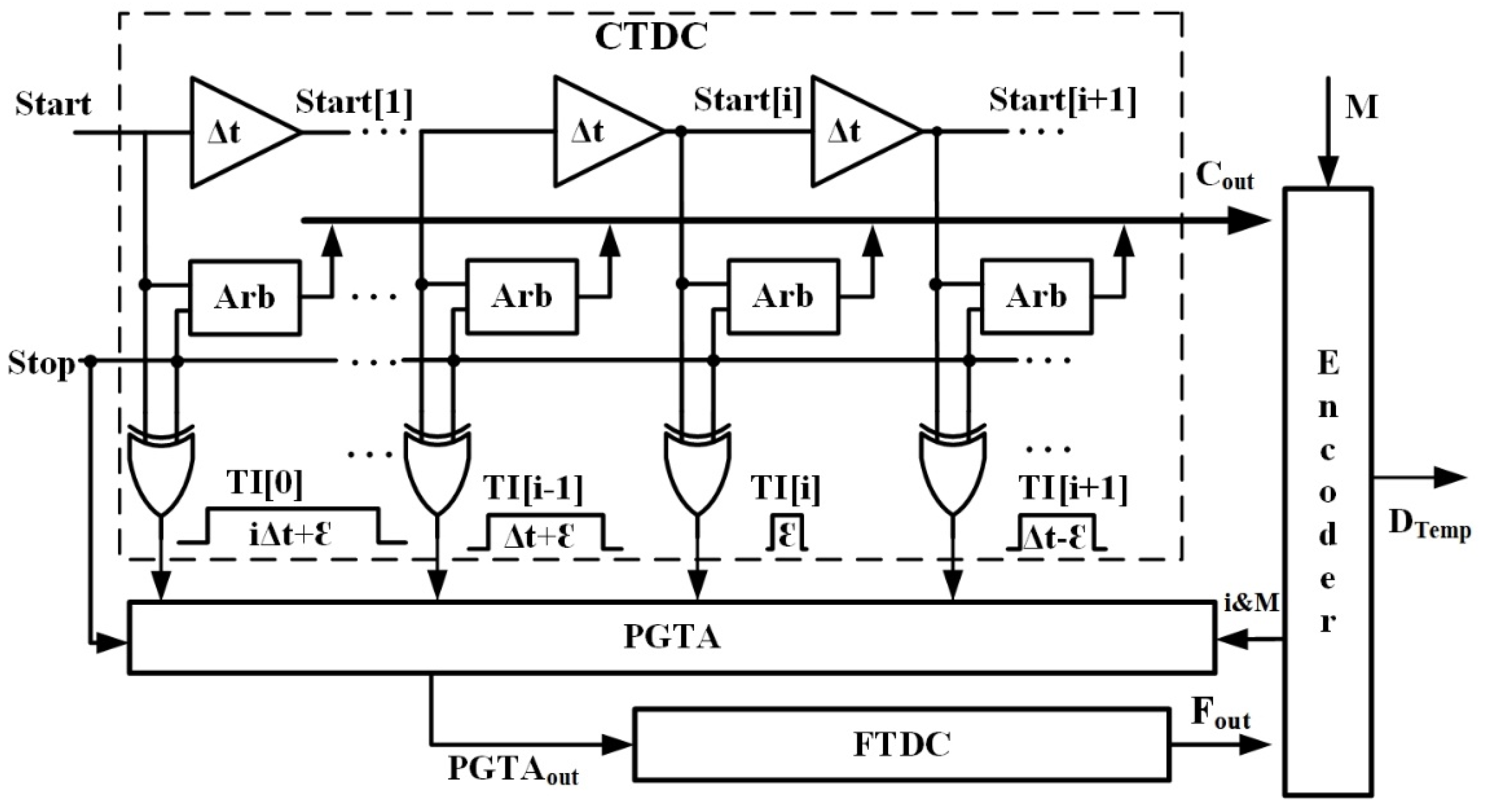
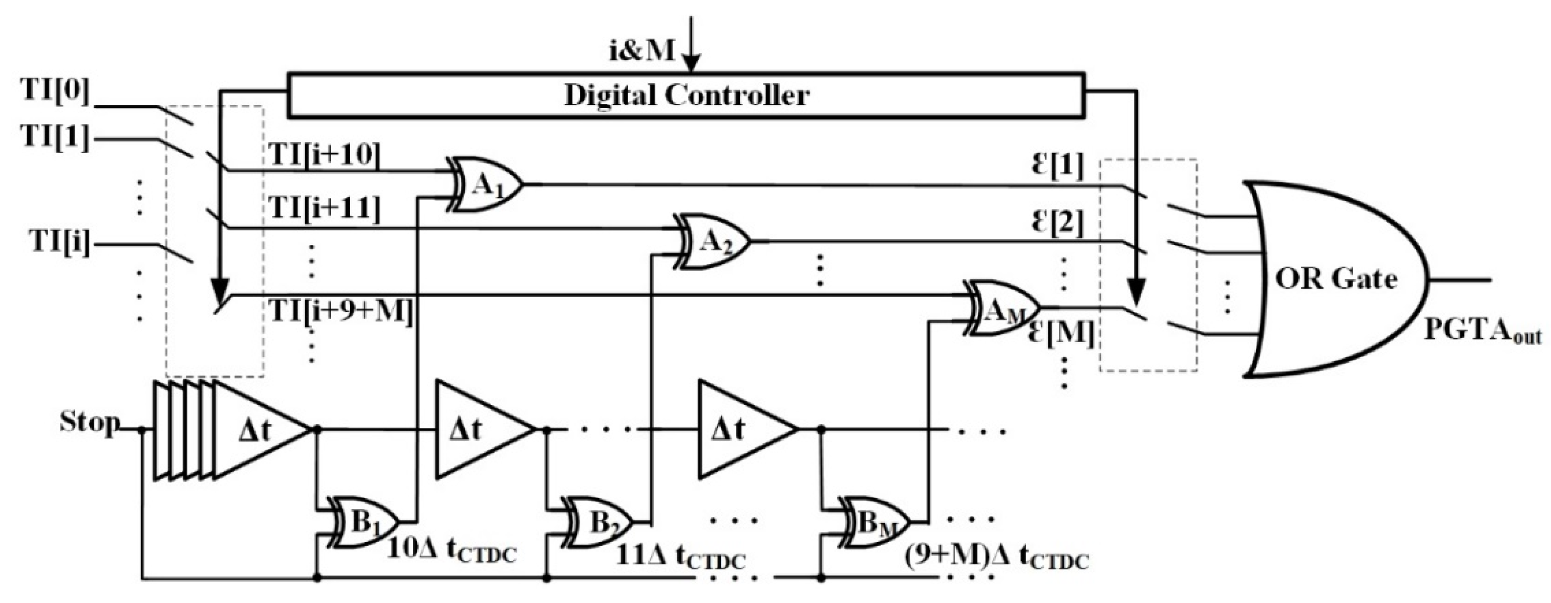
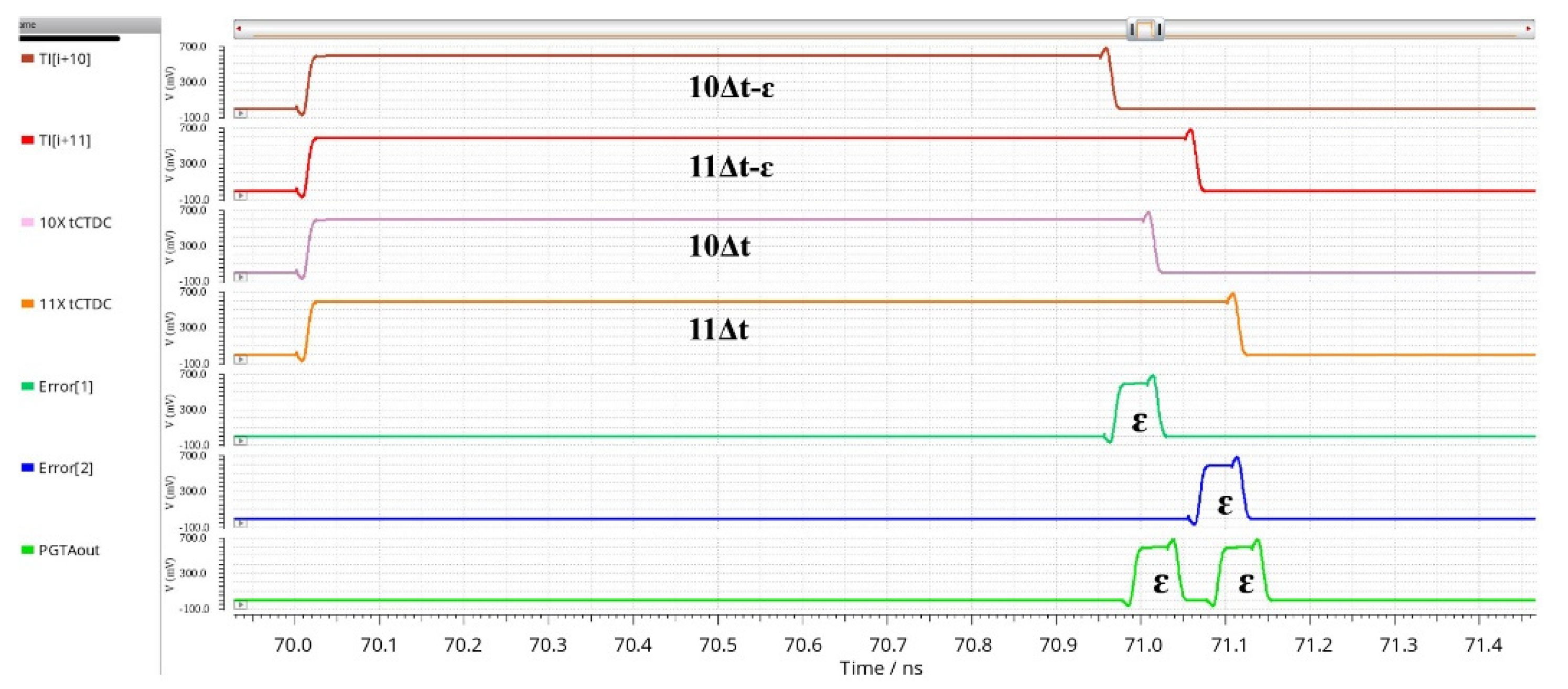
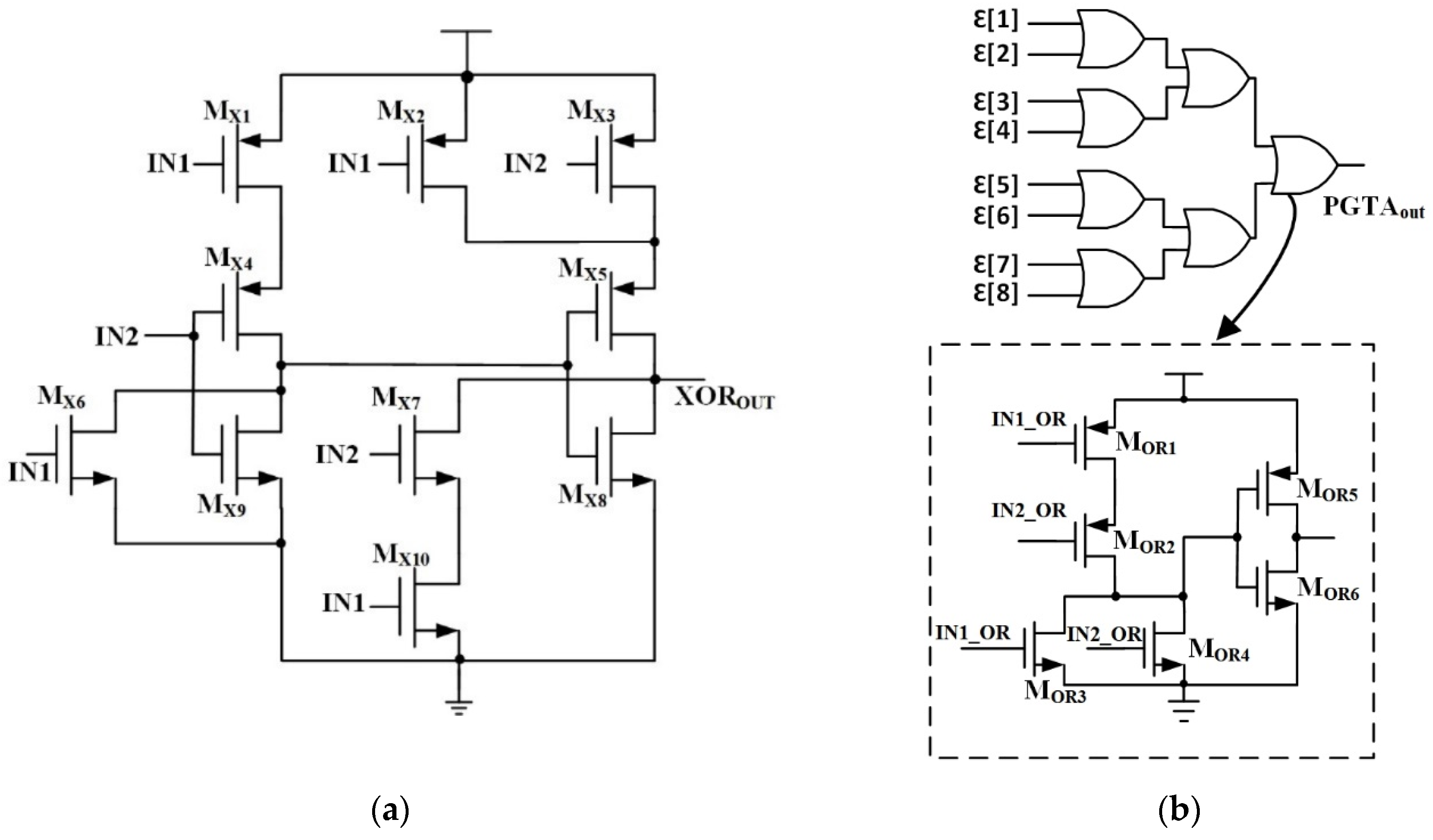
In this paper, we propose a MOSFET-based time domain temperature sensor, which is suitable for BIoT applications due to its short conversion time and high energy efficiency. The architecture diagram of this work is shown in Figure 2. The sensing module uses a delay line to convert the temperature information into a delay time. An offset compensator generates a delay signal with low temperature sensitivity, which can compensate the offset part of the sensing module output. The output delay difference between the sensing module and the offset compensator is then translated into a corresponding digital code using a pipeline TDC. A programmable-gain time amplifier (PGTA) is proposed to achieve an integer time gain and it is low sensitive to temperature variation. The PGTA has a high linearity, a wide linear range, and a programmable time gain. Implemented in a 40 nm standard CMOS technology, the prototype sensor consumes 7.6 μA at a 0.6 V supply and achieves a 90 K resolution from –20 °C to 80 °C at a short conversion time of 1.3 μs.
The remainder of this paper is organized as follows. Section 2 describes the operation principles and the theory analysis. Section 3 presents circuit implementations with detail analysis. Section 4 shows the measurement results of this work, and in Section 5, we present the conclusions for this paper.

2. Principles of Operation and Theory Analysis

For time-domain temperature sensors, the most common method of temperature sensing is to use one or more delay lines to convert the temperature information into a time-domain signal. Therefore, it is necessary to analyze the temperature characteristics of the delay unit which is used in the sensing module and the TDC. According to [9], the process of an inverter output transiting from high to low and from low to high can be equivalent to the process of the load capacitor charging and discharging through the equivalent resistance of MOSFET. At this point, if the output voltage is taken as half of the supply voltage as the reference point, the propagation delay can be expressed as
{ t P H L = ln 2 R N C L t P L H = ln 2 R P C L ,
where RP and RN are the equivalent resistances of PMOS and NMOS, respectively, at the ON state. CL is the load capacitance of the inverter, which has a low-temperature sensitivity [7,8]. The temperature characteristic of the delay time thereby depends on RP and RN that can be written by
R N = 2 V D D 2 V D D V D D V D S I D S ( 1 + λ V D S ) d V 3 4 V D D I D S ( 1 7 9 λ V D D ) ,
R P = 2 V D D V D D 2 V D D V D S I D S ( 1 + λ V D S ) d V 3 4 V D D I D S ( 1 7 9 λ V D D ) ,
where VDD, VDS, IDS, and λ are the supply voltage, drain-source voltage, drain-source current and channel length modulation coefficient, respectively.
Considering that the MOSFETs operates in triode region when the output voltage transits from initial value to 1/2VDD, ignoring the influence of other non-ideal factors, the drain current can be expressed as follows:
I D S = 1 2 μ C O X w L { ( V D D V T H ) V D S 1 2 V D S 2 } ,
where µ is the carrier mobility, COX is the gate-oxide capacitance per unit area, W and L are the channel width and length of MOSFET, and VTH is the threshold voltage. According to the analysis in References [10,11]:
μ = μ 0 ( T T 0 ) γ ,     γ = 1.2 ~ 2.2 ,
V T H = V T H 0 + a ( T T 0 ) ,           a = 2 ~ 7   mV / K ,
where T0 is the reference temperature, µ0 is the carrier mobility at reference temperature, VTH0 is the threshold voltage at reference temperature, and T is the temperature.
With a rise of temperature, the mobility and the threshold voltage will both decrease. The change of drain current with respect to temperature is obtained by derivation of the Equation (5) to temperature.
d I D S d T = 1 2 w L C O X [ ( V D D V T H ) V D S 1 2 V D S 2 ] d μ d T 1 2 w L μ C O X V D S d V T H d T .
Since dμ/dT < 0 and dVTH/dT < 0, the temperature characteristics of the drain-source current can be determined by VDDVTH, affected by the anti-short channel effect of MOSFET, the threshold voltage decreases with the increase of channel length. Therefore, when the channel length is long, VTH is much smaller than VDD. In this case, the temperature characteristics of the drain current will be controlled by the carrier mobility, that is, thermal coefficient of the drain current is negative. Otherwise, a shorter channel length will make the thermal coefficient of drain current positive.
By substituting Equations (3)–(5) into Equation (2), the delay time of inverter can be obtained:
{ t P H L = 3 ln 2 C L V D D ( 1 7 9 λ V D D ) 2 μ N C O X w L { ( V D D V T H ) V D S 1 2 V D S 2 } t P L H = 3 ln 2 C L V D D ( 1 7 9 λ V D D ) 2 μ N P C O X w L { ( V D D V T H ) V D S 1 2 V D S 2 } .
The delay time of a delay unit composed of two inverters is shown in Equation (10), which is inversely proportional to the drain current. According to Equation (8), with the change of the channel length of MOSFETs, the delay unit can generate a delay time that is positively or negatively correlated with temperature.
t d e l a y _ u = t P H L + t P L H .
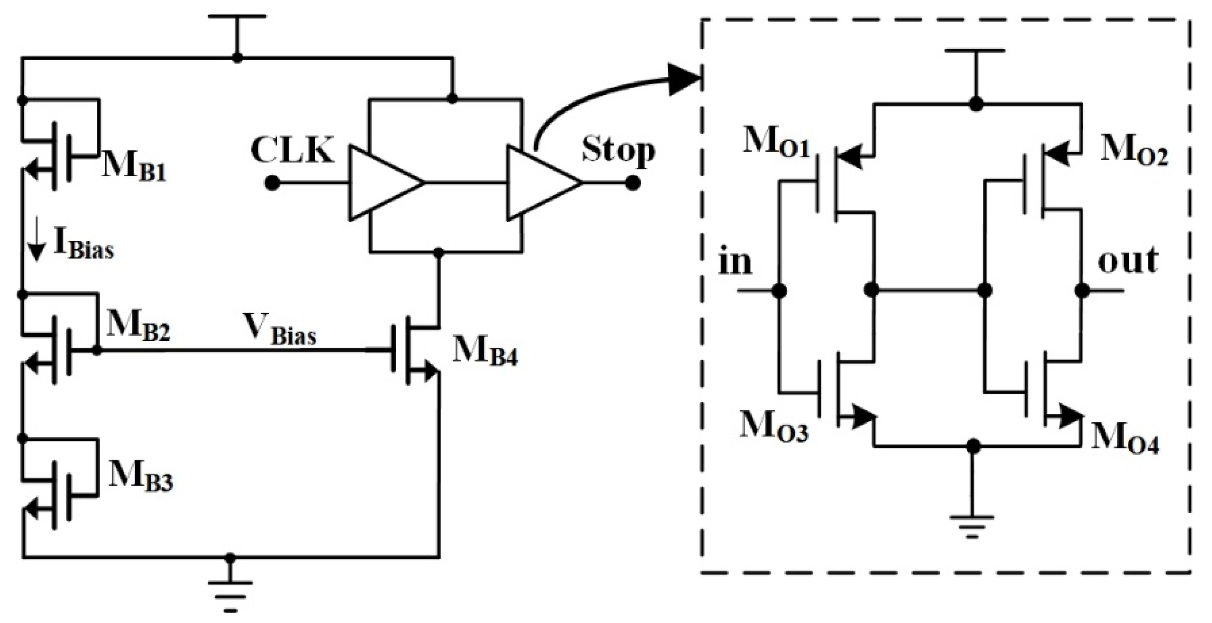
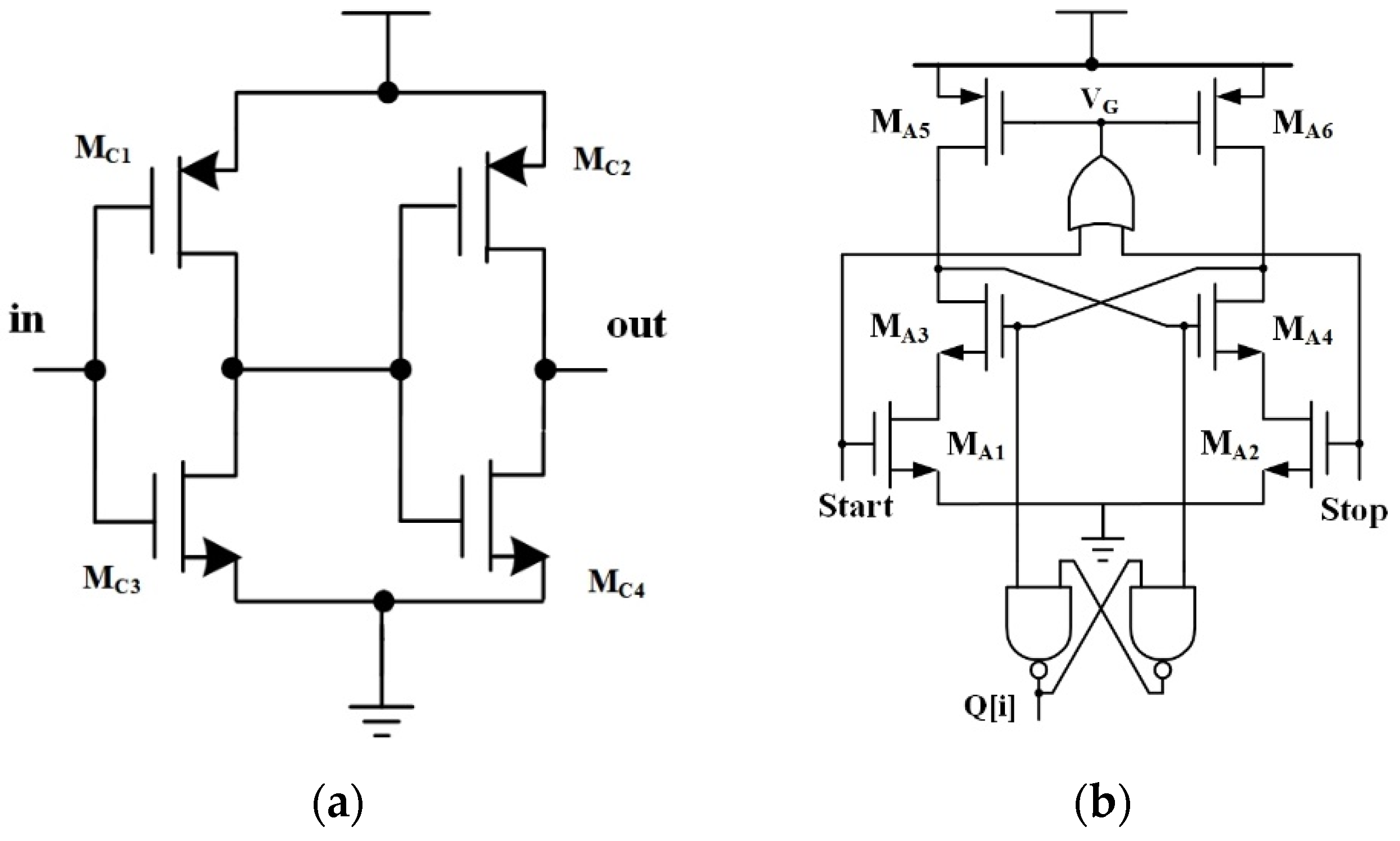
In the range of the temperature measurement, the propagation delay of the sensing module has a part of offset. If this signal is directly quantized by a TDC, it will greatly increase the number of the delay units in the TDC and furthermore lead to an additional area and a longer conversion time, which increases the effective power and the area of the sensor and is not suitable for the BIoT applications. To solve this problem, an offset compensator is used to generate a delay signal with low temperature sensitivity to compensate the offset part and the structure is shown in Figure 3.
In order to reduce the power consumption of the bias circuit in the offset compensator, the bias circuit works in sub-threshold region. The drain current of a MOSFET operating in sub-threshold region is shown as
I D S = μ W L C d V T 2 exp ( V G S V T H n V T ) [ 1 exp ( V D S V T ) ] ,
where n is the sub-threshold slope and it is larger than one under the normal circumstances. VT is the thermal voltage, and its relationship with temperature is
V T = k T q       ( k = 1.3806 × 10 23   J / K ) ,
when VDS ≥ 4VT, the Equation (11) can be simplified as
I D S = μ W L C d V T 2 exp ( V G S V T H n V T ) .
As shown in Figure 3, the offset compensator consists of four MOSFETs and delay units, MB1, MB2, and MB3 are working in sub-threshold region, and MB2 and MB3 have the same size. According to Equation (13), the IBias and VBias are shown as
I B i a s = μ W 1 L 1 C d V T 2 exp ( V G S 1 V T H 1 n V T ) ,
V G S 2 = ln [ u n w 1 L 1 C d V T 2 u n w 2 L 2 C d V T 2 exp ( V G S 1 V T H 1 n V T ) ] n V T + V T H 2 = n V T ln ( w 1 L 2 L 1 w 2 ) + V G S 1 V T H 1 + V T H 2 .
In the offset compensator, M2 and M3 have the same size. Therefore,
V b i a s = 2 V G S 2 = 2 [ n V T ln ( w 1 L 2 L 1 w 2 ) + V G S 1 V T H 1 + V T H 2 ] .
With the same CMOS process, the temperature coefficients of VTH1 and VTH2 are approximately same. Therefore, the temperature characteristics of VBias is determined by VT. By changing the size of MB1 and MB2, VBias that is proportional to temperature is generated. For delay units in the offset compensator, choosing MOSFETs with a longer channel length can increase the propagation time. According to Equation (8), this means the current of the delay units in the offset compensator is inversely proportional to temperature. With the control of VBias, the drain current of MB4 will be positively correlate with the temperature, thereby this can reduce the temperature sensitivity of propagation delay of the offset compensator. Note that the linearity of the offset compensator is more important than the temperature sensitivity of the offset compensator, because the sensitivity is not required to be exactly zero. In this work, the slope of the delay-temperature curve in the sensing module is 0.141 ns/°C, where that in the offset compensator is 0.059 ns/°C, which is translated to a 0.081 ns/°C slope of the temperature sensor.

3. Circuit Design Implementation with Operation Details

3.1. Sensing Module

The proposed temperature sensor uses a delay line as the sensing module. The structure of the delay unit in the sensing module is shown in Figure 4. After the CLK signal passes through the sensing module, a temperature-dependent delay is generated. For the sensing module with N delay units, the propagation delay can be expressed as
t s e n s o r = N × t d e l a y _ u .
As mentioned above, the temperature characteristics of the propagation delay depends on carrier mobility and threshold voltage. According to Equations (9) and (10), in order to achieve a higher resolution, the variation range of the propagation delay with respect to the temperature should be larger. Therefore, it is necessary to increase the channel length of MOSFET. In order to meet the various demands of BIoT applications, such as moist heat sterilization, as well as preservation and transport of biomedical samples, the temperature range of the sensor is designed from −20 °C to 80 °C. The sensing module is designed to generate a 60~73 ns propagation delay over the temperature range of –20~80 °C when L = 11 µm. The propagation delay is approximately proportional to the temperature. The delay difference between the sensing module and the offset compensator is 13~22 ns over the temperature range of −20~80 °C. Figure 5 shows the response ((t’sensor −t−20)/t−20, where t’sensor is the propagation delay change of the sensing module after compensation, t−20 is the propagation delay of the sensing module after compensation at −20 °C) of the temperature sensor with variation in temperature from −20 °C to 80 °C. It can be clearly seen from Figure 5 that the temperature sensor demonstrates around 62% change in the delay time of the sensing module after compensation and the sensitivity is 0.62%/°C.

3.2. Pipeline TDC

A delay difference which is proportional to temperature is generated after a CLK signal propagating the sensing module and the compensator. It is the most convenient way to quantize the delay difference using a TDC. Taking account of the requirements of the area and the resolution for the BIoT applications, a pipeline structure is used in this work. The structure of the proposed TDC is shown in Figure 6, which is composed of a coarse TDC (CTDC), a PGTA, a fine TDC (FTDC), and an encoder.

3.2.1. CTDC

As shown in Figure 6, the CTDC is based on a traditional delay-line structure. The structure of the delay unit in the CTDC is shown in Figure 7a. In order to avoid introducing additional errors, the temperature sensitivity of a delay unit in the CTDC should be as low as possible. According to Equation (8), by carefully designing the channel length of MOSFET to adjust the VTH, the propagation delay of a delay unit in the CTDC can maintain low temperature sensitivity. The VTH can be expressed as
V T H = V D D μ d V T H d T d μ d T + 1 2 V D S .
The simulation results of the delay unit variations in the CTDC under different processes are shown in Figure 8. It can be seen that the resolution of the CTDC is 100.6–101.5 ps at the NMOS-Typical corner and PMOS-Typical corner (TT corner) when L = 170 nm. The worst condition occurs at the NMOS-Slow corner and PMOS-Slow corner (SS corner), which shows a delay variation less than 3.8 ps over the temperature range of −20~80 °C. Comparing with the resolution of 117~121.2 ps at SS corner, the variation is about 2.54%. The effect on quantization result caused by the variation is negligible.
The structure of the arbiter is shown in Figure 7b. Note that the OR gate output VG exhibits only a slim strip of low-level voltage when the phase difference between Start and Stop is approximately π. This results in MA5 and MA6 having insufficient time to charge their drain terminals prior to the next detection. Therefore, a certain margin is required to guarantee the proper functioning of the arbiter circuit. However, this limitation mostly has no effect in this work. The time difference between Start and Stop is less than 22 ns, which implies a frequency lower than 23 MHz should be used in the circuit. In this work, a real-time clock (32.768 kHz) is used for the input clock (CLK in Figure 2).

3.2.2. PGTA

Time amplifier (TA) is a key module in a pipeline TDC, which amplifies the residue generated in the CTDC quantization. A TA determines the measurement accuracy of a pipeline TDC. The SR-latch-based TA [12] and the cross-couple structure [13] had a very narrow linear range due to the metastable work region and limited discharging time, respectively. A closed-loop TA [14] had a wider input linear range than SR-latch structure, but the gain is not programmable. A promising TA [15] achieved time amplification by duplicating the residue in an OR gate, providing a wide input linear range and a programmable gain simultaneously. However, long delay lines were used in the TA to shift the residues, which caused possible overlaps between each two adjacent residues due to the temperature-dependent delay lines and thus resulted in reducing the accuracy of the amplification. In addition, the long delay lines also slowed down the conversion time.
In the existing works [12,13,14], the TAs amplified the residue in the stage where the stop catches up with the start, the position is defined as stage i, as shown in Figure 4. In fact, the residue exists in every stage of the delay line in CTDC. For instance, the time interval between Start [i+1] and Stop is (△tCTDC-ε), where ε is the residue and △tCTDC is the delay time of a delay unit in the CTDC. In the proposed PGTA, time amplification is achieved by extracting M times intervals in M different stages, and the residue is thereby amplified by M times. As shown in Figure 9, the PGTA is composed of a delay line, a digital controller, an OR gate and two groups of XOR gates. According to the PGTA gain (M) and i, the signals from TI[i+10] to TI[i+9+M] are selected by the digital controller. In this work, M is the gain of the PGTA, and M ≤ 8. The XOR gates in the group B are used to extract pulse signals, whose pulse width equal a replication of several times △tCTDC from 10 × △tCTDC to (9+M) × △tCTDC. The pulses TI selected by the digital controller and the outputs of the XOR gates in Group B are send into the XOR gates in Group A. Thus, the residuals are extracted. To guarantee accurate pulse widths of the residues, the size of each delay unit in the PGTA is exactly as same as that in the CTDC. The OR gate sums the pulses (from ε[1] to ε[M]) and generates a serial signal composed of M residues in which each single pulse width is ε. Therefore, the residue is amplified by M times. The simulation of the PGTA when M = 2 is shown in Figure 10. The ideal resolution of the temperature sensor can be expressed as
R e s o l u t i o n T E M P = t F T D C × T r a n g e t t e m p × M ,
where △ttemp is the range in which the output delay difference between the compensator and the sensor module with temperature variations, tFTDC is the propagation delay of the delay unit in FTDC, and Trange denotes the temperature range (−20~80 °C) in this work.
The structure of the XOR gate and the OR gate in the PGTA is shown in Figure 11. The matching between the rising edges and falling edges of the XOR gates and the OR gate determines the amplification accuracy of the PGTA. For the CMOS logic gates, by adjusting the width-to-length ratio of PMOS and NMOS, the matching between the rising edges and the falling edges can be ensured. As the temperature changes, the slopes of the rising edges and falling edges are similar so that the PGTA is low sensitive to temperature variations. In the proposed PGTA, the pulse width variations of a single XOR output is less than 1 ps over the temperature range of −20~80 °C.

3.2.3. FTDC

Since the PGTA outputs a serial discrete pulses, a FTDC based on a gate delay line (GDL) is used to quantize the amplified residues. The structure of FTDC is shown in Figure 12. The PGTA output is used as an Enable signal to control the propagations of a LP signal in the GDL. The statement of each delay unit in the GDL is read by the encoder as the output of the FTDC. With the control of LP and LP_n signal, MF9 and MF10 is used to reset the statement of the FTDC after quantization. According to the descriptions in Section 3.2.1, the sizes of the MOSFETs are carefully designed to ensure that the delay units in the FTDC maintain a low temperature sensitivity. The resolution of the FTDC is about 50 ps. Note that the quantized range of the FTDC should be larger than the total output pulse width of the PGTA. In this work, the FTDC is composed of 32 stages delay units, which can provide a 1.6 ns quantized range.

3.3. Post-Simulation

One important design consideration is that the delay difference between the sensing module and the offset compensator should not exceed the quantized range of the pipeline TDC that is determined by the CTDC. In the proposed TDC, the number of stages of CTDC is 256 and the maximal gain of PGTA is 8 in this work. In order to work properly, eight stages after the stage [i+10] in the CTDC are used to extract the residues to guarantee a sufficient processing time for the Encoder when M = 8. Thereby, the effective number of the stages in the CTDC is 237. The maximum conversion time of the CTDC is determined by M and the location where i occurs, which can be expressed as
T c o n v C T D C = ( i + 9 + M ) × t   C T D C , 130 < i < 220 .
According to the simulation results, the maximum i is 220, at 80 °C. Therefore, the conversion time of the CTDC is about 23.937 ns. The possible maximum conversion time of CTDC is 25.856 ns when i = 237 and M = 8.
The post-simulation result of the temperature sensor output is shown in Figure 13 at different process corners. Thanks to the low temperature sensitivity design of the pipeline TDC, the output has the best linearity at the TT corner. The non-linearity under other process corners is mainly caused by the temperature sensitivity variations of the delay unit in the CTDC and the FTDC. The difference non-linearity (DNL) of the temperature sensor output is shown in Figure 14a and the DNL is from −0.6 LSB to 0.7 LSB. The integral non-linearity (INL) of the temperature sensor output is shown in Figure 14b and the INL is from −1.3 LSB to 2.6 LSB.
The error after one-point calibration is shown in Figure 15a. Matlab® is used to find the best fitted lines for the five output curves at different corners. At the NMOS-Fast corner and PMOS-Fast corner (FF corner) and SS corner, as shown in Figure 8, the propagation delay of delay unit is proportional and inversely proportional to the temperature respectively, thereby the second order temperature coefficient of the temperature sensor output is positive and negative, respectively. The error curves at the other corner are between those at FF and SS corners. After two-point calibration, the result is shown in Figure 15b. The worst condition occurs at SS corner, which shows an error of 0.9 °C. At the TT corner, the maximum error is less than 0.29 °C. The design parameters used in this work are summarized in Appendix A.

4. Experimental Results

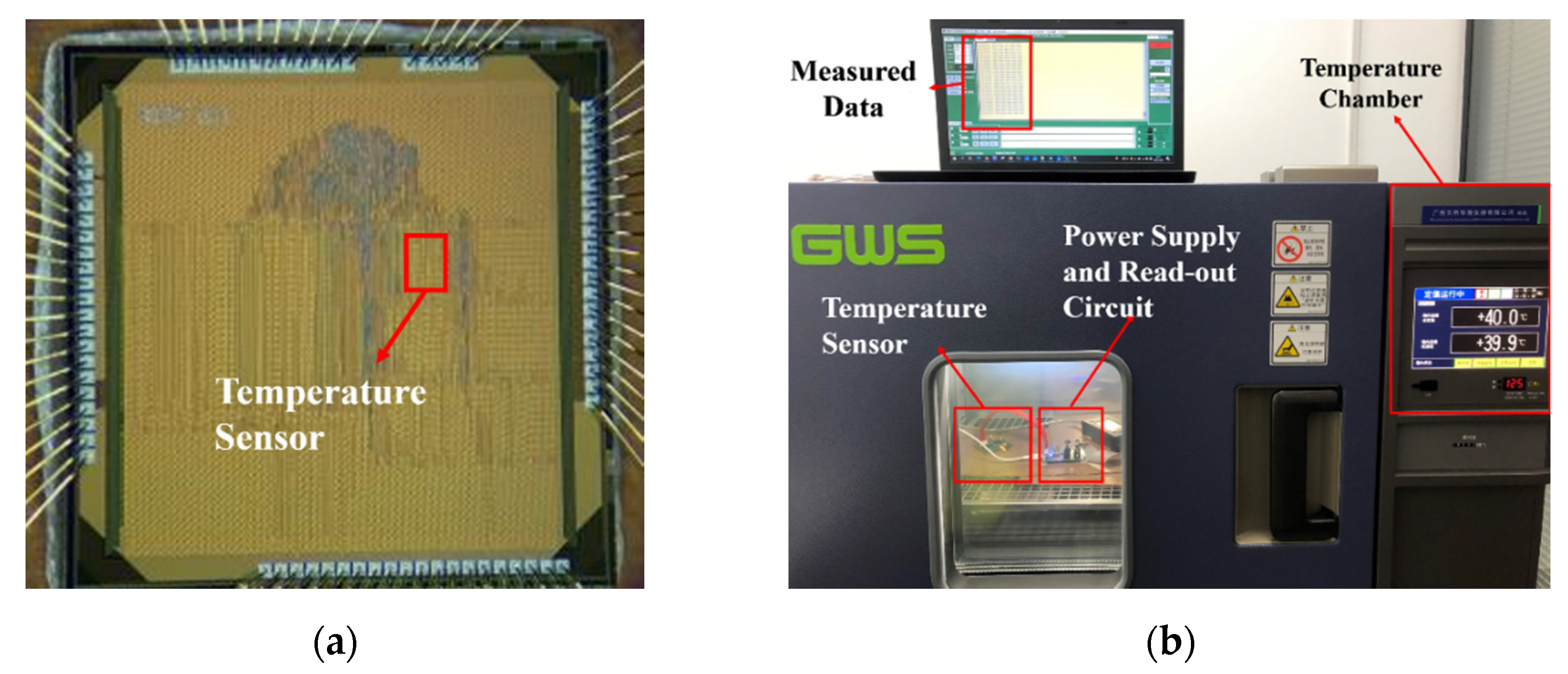
The proposed temperature sensor was fabricated in a TSMC 40-nm standard CMOS technology and worked at a 0.6 V supply voltage. The total area of this sensor is 0.05 mm2, as shown in the die micrograph in Figure 16a. A photograph of the testing environment is shown in Figure 16b. The sensor was mounted on a test board and placed in a temperature chamber manufactured by GWS. The test board was connected to a power supply and read-out circuit. A computer placed outside the temperature chamber was connected to the read-out circuit, and the output code was read every 10 °C.
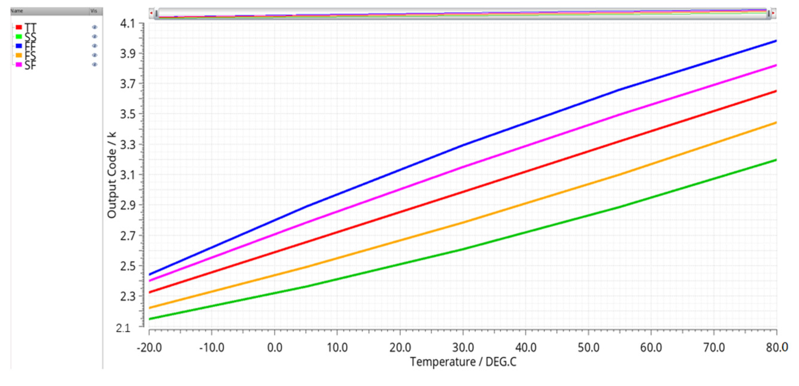
The 
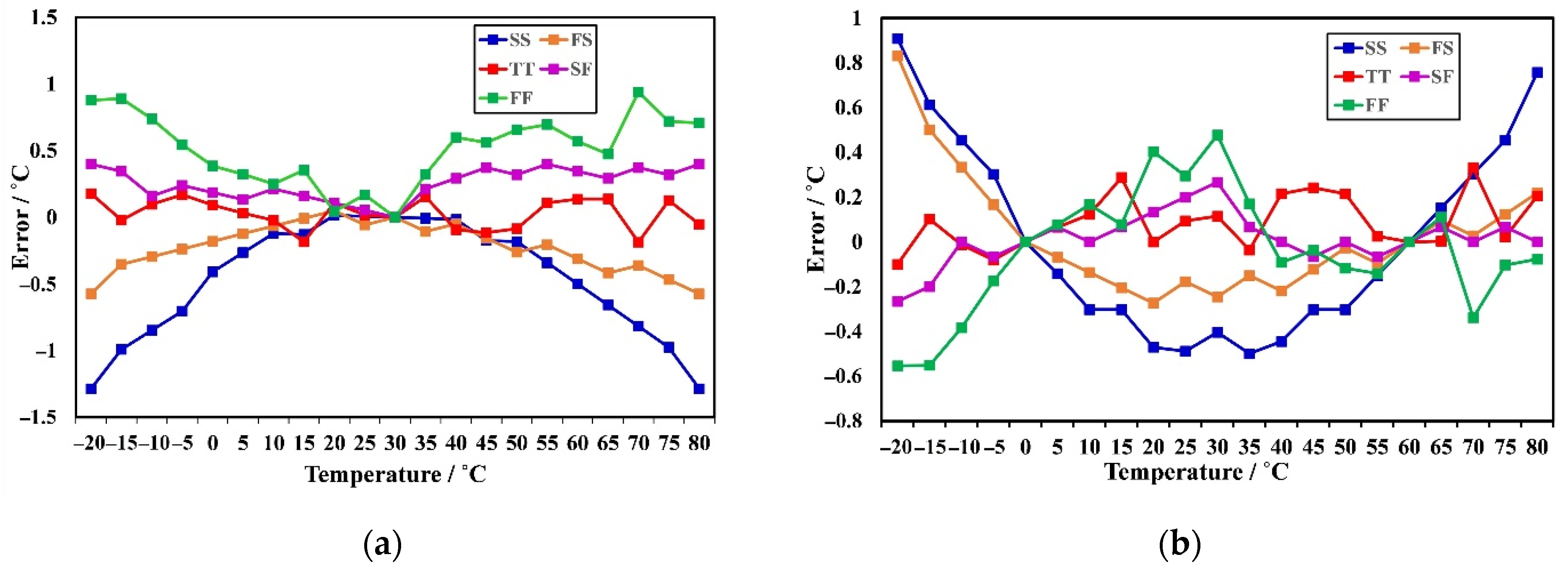
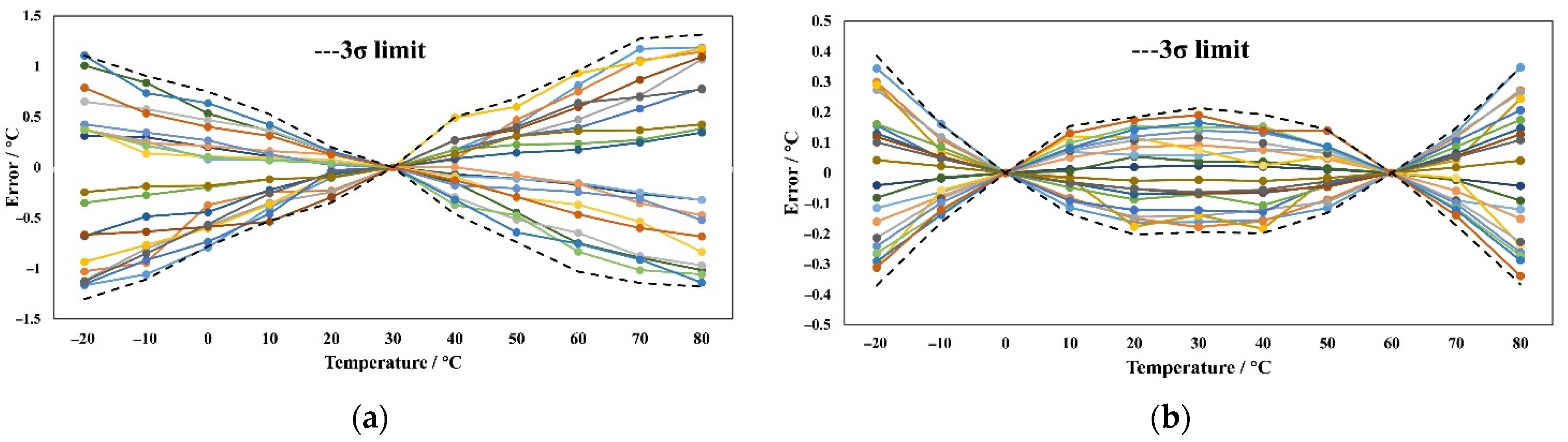
Figure 17 shows the simulated output results and the measured output results with different PGTA gains. When M = 8, 20 samples from one wafer are tested in the temperature chamber over the temperature range of −20~80 °C. The error measurements of the proposed temperature sensor with one-point and two-point calibration are shown in 
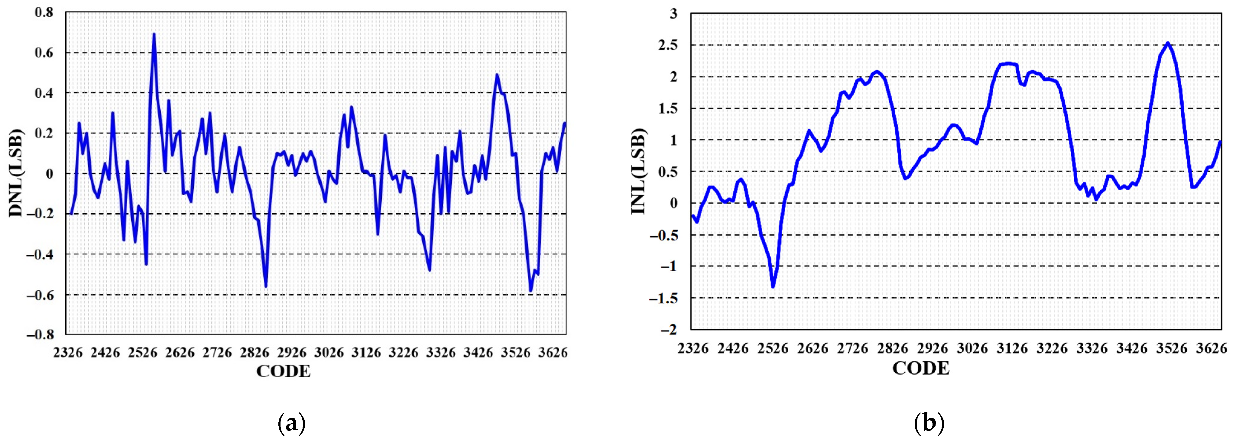
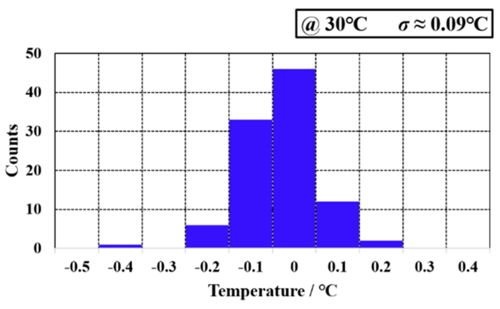
Figure 18a,b, respectively. With one-point calibration at 30 °C, the measured peak-to-peak errors is ±1.3 °C. In the case of a two-point calibration, the calibration temperatures are selected to 0 °C and 60 °C, and the measured peak-to-peak nonlinearity is ±0.39 °C. The sensor resolution is obtained by measuring the spread of sensor error at 30 °C, as shown in Figure 19. The standard deviation of the measurement is about 0.09 °C.
Table 1 summarizes the measured temperature sensor performance and compares it with other state-of-the-art works. Reference [16] has the highest resolution and a high FoM at the cost of long conversion time and large area. Reference [17] has a similar high resolution with Reference [16] and small area at the cost of high power and long conversion time. This work achieves the best FoM of 0.048 pJ·K2 thanks to the shortest conversion time of 1.3 µs.

5. Conclusions

We proposed a CMOS time-domain temperature sensor in this paper. The relationship between the temperature characteristic of propagation delay and the size of a delay unit is analyzed. The design of the channel length of MOSFET can determine the positive or negative temperature coefficient of the propagation delay. Based on this principle, the temperature is converted into a PTAP time domain signal, and then a pipeline TDC is used to quantize the signal. A PGTA is proposed to achieve linear programmable gain. In order to avoid introducing additional errors and to improve the linearity of the TDC output, the circuits in the TDC are designed with low temperature sensitivity. Thus, this temperature sensor does not need any curvature corrections.
Based on the analysis and design, a temperature sensor had been fabricated in a 40-nm CMOS technology. A 90 mk resolution at an eight times PGTA gain was achieved. The conversion time is only 1.3 µs, and a FoM of 48 fJ·K2 is obtained.
For most BIoT applications, the temperature does not change fast, therefore, a low sampling rate of the temperature sensor can meet the demand of the system that works at a duty-cycling mode. In the sleep mode, the sensor only draw 31 nA at 40 °C. At 10 conversions/s and Tconv = 1.3 µs, the effective average power consumption is only 18.6 nW. In order to apply this sensor to different applications, a higher-stages of sensing module can be used to increase the range of propagation delay varying with temperature to achieve a higher resolution.

Author Contributions

Conceptualization, Z.C. and Z.W. (Ze Wang); Data curation, Z.W. (Ze Wang); Formal analysis, W.Z. and X.W.; Funding acquisition, Z.C. and Z.W. (Zixuan Wang); Writing—original draft, Z.W. (Ze Wang); Writing—review & editing, Z.C. and Z.W. (Zixuan Wang). All authors have read and agreed to the published version of the manuscript.

Funding

This research was funded by the National Natural Science Foundation of China, grant number 61504061 and 61974073; the National Key Research and Development Program of China, grant number 2018YFB2202005.

Data Availability Statement

Data is contained within the article.

Conflicts of Interest

The authors declare no conflict of interest.

Appendix A

The design parameters used in this work are summarized in Table A1.
Table A1. Design parameters used in this work.
ComponentsParametersComponentsParametersComponentsParameters
Supply0.6 VMC1 4480 nm/170 nmMX4 6480 nm/40 nm
Ms1 1240 nm/11 μmMC2 4480 nm/170 nmMX5 6240 nm/40 nm
Ms2 1240 nm/11 μmMC3 4240 nm/170 nmMX6 6120 nm/40 nm
Ms3 1120 nm/11 μmMC4 4240 nm/170 nmMX7 6120 nm/40 nm
Ms4 1120 nm/11 μmMA1 5120 nm/40 nmMX8 6120 nm/40 nm
MB1 22.64 μm/40 nmMA2 5120 nm/40 nmMX9 6120 nm/40 nm
MB2 2120 nm/10 μmMA3 5120 nm/40 nmMX10 6120 nm/40 nm
MB3 2120 nm/10 μmMA4 5120 nm/40 nmMOR1 7480 nm/40 nm
MB4 23 μm/500 nmMA5 5240 nm/40 nmMOR2 7480 nm/40 nm
MO1 34.32 μm/4.4 μmMA6 5240 nm/40 nmMOR3 7120 nm/40 nm
MO2 34.32 μm/4.4 μmMX1 6480 nm/40 nmMOR4 7120 nm/40 nm
MO3 32.16 μm/4.4 μmMX2 6120 nm/40 nmMOR5 7240 nm/40 nm
MO4 32.16 μm/4.4 μmMX3 6120 nm/40 nmMOR6 7120 nm/40 nm
1 MS: the MOSFET in the delay units of the sensing module; 2 MB: the MOSFET in the offset compensator; 3 MO: the MOSFET in the delay units of the offset compensator; 4 MC: the MOSFET in the delay units of CTDC; 5 MA: the MOSFET in the arbiters of CTDC; 6 MX: the MOSFET in the XOR gates; 7 MOR: the MOSFET in the OR gate of the PGTA.

References

  1. Chouhan, S.S.; Halonen, K. A 40 nW CMOS-Based Temperature Sensor with Calibration Free Inaccuracy within ±0.6 °C. Electronics 2019, 8, 1275. [Google Scholar] [CrossRef] [Green Version]
  2. Sebastiano, F.; Breems, L.J.; Makinwa, K.A.; Drago, S.; Leenaerts, D.M.; Nauta, B. A 1.2 V 10 μW NPN-based temperature sensor in 65 nm CMOS with an inaccuracy of 0.2 °C (3 s) from −70 °C to 125 °C. IEEE J. Solid State Circuits 2010, 45, 2591–2601. [Google Scholar] [CrossRef] [Green Version]
  3. Soni, M.; Bhattacharjee, M.; Ntagios, M.; Dahiya, R. Print Temperature Sensor Based on PEDOT: PSS-Graphene Oxide Composite. IEEE Sens. J. 2020, 20, 7525–7531. [Google Scholar] [CrossRef] [Green Version]
  4. Anand, T.; Makinwa, K.A.A.; Hanumolu, P.K. A VCO based highly digital temperature sensor with 0.034 °C/mV supply sensitivity. IEEE J. Solid State Circuits 2016, 51, 2651–2663. [Google Scholar] [CrossRef]
  5. Li, J.; Lin, Y.Y.; Ning, N.; Yu, Q. A +0.44_C/−0.4_C Inaccuracy Temperature Sensor with Multi-Threshold MOSFET-Based Sensing Element and CMOS Thyristor-Based VCO. IEEE Trans. Circuits Syst. I Regul. Pap. 2021, 68, 1102–1113. [Google Scholar] [CrossRef]
  6. Pan, S.; Luo, Y.Q.; Shalmany, S.H.; Makinwa, K.A.A. A Resistor-Based Temperature Sensor with a 0.13 pJ·K2 Resolution FoM. IEEE J. Solid State Circuits 2018, 53, 164–173. [Google Scholar] [CrossRef] [Green Version]
  7. Chen, P.; Chen, C.C.; Tsai, C.C.; Lu, W.F. A Time-to-Digital-Converter-Based CMOS Smart Temperature Sensor. IEEE J. Solid State Circuits 2005, 40, 1642–1648. [Google Scholar] [CrossRef]
  8. Chen, C.C.; Chen, H.W. A Low-Cost CMOS Smart Temperature Sensor Using a Thermal-Sensing and Pulse Shrinking Delay Line. IEEE Sens. J. 2014, 14, 278–284. [Google Scholar] [CrossRef]
  9. Rabaey, J.M.; Chandrakasan, A.; Nikolic, B. Digital Integrated Circuits: A Design Perspective, 2nd ed.; Pearson Education, Inc.: Boston, MA, USA, 2003; pp. 199–200. [Google Scholar]
  10. Filanovsky, I.M.; Allam, A. Mutual compensation of mobility and threshold voltage temperature effects with applications in CMOS circuits. IEEE Trans. Circuits Syst. I Regul. Pap. 2001, 48, 876–884. [Google Scholar] [CrossRef]
  11. Filanovsky, I.M. Voltage reference using mutual compensation of mobility and threshold voltage temperature effects. In Proceedings of the IEEE International Symposium on Circuits and Systems (ISCAS), Geneva, Switzerland, 28–31 May 2000. [Google Scholar]
  12. Lee, M.; Abidi, A.A. A 9 b, 1.25 ps resolution coarse-fine time-to-digital converter in 90 nm CMOS that amplifies a time residue. IEEE J. Solid State Circuits 2008, 43, 769–777. [Google Scholar] [CrossRef]
  13. Lee, S.K.; Seo, Y.H.; Suh, Y.J.; Sim, J.Y. A 1 GHz ADPLL with a 1.25 ps minimum-resolution subexponent TDC in 0.18 μm CMOS. IEEE J. Solid State Circuits 2010, 45, 2874–2881. [Google Scholar] [CrossRef]
  14. Mandai, S.; Charbon, E. A 128-Channel, 8.9-ps LSB, Column-ParallelTwo-Stage TDC Based on Time Difference Amplification for Time-Resolved Imaging. IEEE Trans. Nucl. Sci. 2012, 59, 2463–2470. [Google Scholar] [CrossRef]
  15. Wang, Z.; Ding, H.; Xu, H.; Zhang, C.; Hu, S.; Ji, X.; Xia, X.; Cai, Z. An all-digital phase-locked loop with a PGTA-based TDC and a 0.6-V DCO. IEICE Electron. Express 2018, 15, 1–11. [Google Scholar] [CrossRef]
  16. Jiang, H.; Huang, C.-C.; Chan, M.R.; Hall, D.A. A 2-in-1 Temperature and Humidity Sensor with a Single FLL Wheatstone-Bridge Front-End. IEEE J. Solid State Circuits 2020, 55, 2174–2185. [Google Scholar] [CrossRef]
  17. Choi, W.; Lee, Y.; Kim, S.; Lee, S.; Jang, J.; Chun, J.; Makinwa, K.A.A.; Chae, Y. A Compact Resistor-Based CMOS Temperature Sensor with an Inaccuracy of 0.12 °C (3σ) and a Resolution FoM of 0.43 pJ K2in 65-nm CMOS. IEEE J. Solid State Circuits 2018, 53, 3356–3367. [Google Scholar] [CrossRef]
  18. Wang, A.; Chen, C.X.; Liu, C.; Shi, C.J.R. A 9-Bit Resistor-Based Highly Digital Temperature Sensor with a SAR-Quantization Embedded Differential Low-Pass Filter in 65-nm CMOS with a 2.5-μs Conversion Time. IEEE Sens. J. 2019, 19, 7215–7225. [Google Scholar] [CrossRef]
Figure 1. Operation scenarios of BIoT with (a) an always-on temperature sensor; (b) a duty-cycling temperature sensor.
Electronics 10 01542 g001
Figure 2. Block diagram of the temperature sensor.
Electronics 10 01542 g002
Figure 3. Structure of the offset compensator.
Electronics 10 01542 g003
Figure 4. Structure of the delay unit in the sensing module.
Electronics 10 01542 g004
Figure 5. Simulated delay time of the sensing module and the offset compensator over the temperature range of –20~80 °C.
Electronics 10 01542 g005
Figure 6. Structure of the pipeline TDC.
Electronics 10 01542 g006
Figure 7. (a) Structure of the delay unit in the CTDC; (b) structure of the arbiter in the CTDC.
Electronics 10 01542 g007
Figure 8. Simulated delay time of the delay unit in the CTDC and the variations of the delay time normalized to the resolutions at five different corners. The resolutions are 100.6 ps, 77.8 ps, 94.5 ps, 109.7 ps and 117 ps at TT, FF, SF, FS and SS corners respectively.
Electronics 10 01542 g008
Figure 9. Structure of the PGTA.
Electronics 10 01542 g009
Figure 10. Simulated time diagram of the PGTA at M = 2.
Electronics 10 01542 g010
Figure 11. (a) Structure of the XOR gate; (b) structure of the OR gate in the PGTA.
Electronics 10 01542 g011
Figure 12. Structure of the FTDC.
Electronics 10 01542 g012
Figure 13. Post-simulation results of the temperature sensor outputs at five different corners.
Electronics 10 01542 g013
Figure 14. Linearity of the temperature sensor at TT corner: (a) DNL; (b) INL.
Electronics 10 01542 g014
Figure 15. Post-simulation result of temperature error: (a) after one-point calibration; (b) after two-point calibration.
Electronics 10 01542 g015
Figure 16. (a) Die micrograph; (b) testing environment.
Electronics 10 01542 g016
Figure 17. Simulated and measured output for M = 1, 2, 4, and 8.
Electronics 10 01542 g017
Figure 18. Measured linearity of 20 test chips for (a) one-point calibration at 30 °C; (b) two-point calibration at 0 °C and 60 °C.
Electronics 10 01542 g018
Figure 19. Measured histogram of 100 sensors readings at 30 °C.
Electronics 10 01542 g019
Table 1. Performance comparison of the proposed sensor with state-of-the-art works.
Reference16′ JSSC
[4]
18′ JSSC
[16]
20′ JSSC
[17]
19′ SJ
[18]
This Work
Technology65 nm65 nm180 nm65 nm40 nm
Area/mm20.0040.0070.720.00840.05
Supply/V0.85~1.050.85~1.051.5~2.01.0~1.20.6
Tconv/µs22100010002.51.3
TEMPrange/°C0~100−40~80−40~80−30~100−20~80
Resolution/mK3002.5238090
Inaccuracy/°C0.90.120.551.20.39
Power/µW1546815.635.24.6
1 FoM/pJ·K23000.430.06212.70.048
1 FoM= Power × Conversion Time × Resolution2.
Publisher’s Note: MDPI stays neutral with regard to jurisdictional claims in published maps and institutional affiliations.

