1. Introduction
In many mission- and safety-critical applications such as space, aerospace, nuclear power plants, electric power transmission and distribution, banking and stock exchanges, and industrial control and automation, etc. N-modular redundancy is widely used, with triple modular redundancy (TMR) being common [
1,
2]. To realize a TMR implementation, three identical function blocks are used, where a function block may be a circuit or a sub-system or a system. The corresponding output(s) of the function blocks are majority voted using majority voter(s). Suppose a function block produces K outputs, K 3-input majority voters are required to realize a TMR implementation [
3].
Depending upon the design paradigm adopted, the majority voter used in a TMR implementation may be realized in a synchronous or asynchronous design style. Different designs of majority voters for a synchronous TMR implementation are available in the literature [
4,
5,
6]. Different designs of majority voters for an asynchronous TMR implementation are also available in the literature [
7,
8,
9,
10]. Reference [
7] corresponds to a bundled data asynchronous design while the studies in [
8,
9,
10] correspond to an input-output mode asynchronous design. Generally, an input-output mode asynchronous design is more robust than a bundled data asynchronous design since the former is not delay-sensitive while the latter is sensitive to delays [
11]. Note that henceforth, by ‘asynchronous realization’ we mean an ‘input-output mode asynchronous realization’ in this paper unless stated otherwise.
In [
8,
9], strongly indicating majority voters for an asynchronous TMR implementation were presented while in [
10] an early output majority voter was presented. This paper presents a new, improved early output majority voter for an asynchronous TMR implementation. The dual-rail code is used for data encoding and four-phase return-to-zero handshaking (RTZH) and return-to-one handshaking (RTOH) schemes are separately used for data communication.
The rest of this paper is organized as follows.
Section 2 briefly discusses fundamentals of input-output mode asynchronous circuits.
Section 3 presents the proposed early output majority voter and describes how it is used to realize an efficient asynchronous TMR implementation.
Section 4 gives the design metrics of example TMR implementations which utilize different majority voters including the proposed majority voter.
Section 5 gives the conclusions.
2. Input-Output Mode Asynchronous Circuit
A typical block diagram of an input-output mode asynchronous pipeline stage is shown in
Figure 1a. It consists of a pair of input and output register banks, control signals (AIN and AOUT) which are exchanged between the register banks to control the data flow, an asynchronous circuit that is sandwiched between the register banks, and completion detectors.
In
Figure 1a, an input register bank and an output register bank are shown. The input register bank could serve as an output register bank for a preceding stage in the pipeline, and the output register bank could serve as an input register bank for a successive stage in the pipeline. Supposing that dual-rail encoded signals viz. (A
1,A
0) and (B
1,B
0) are supplied through the input register bank, a two-input C-element is used for each rail of every dual-rail encoded input which is synchronized with the acknowledgment input signal (AIN), and forwarded to the asynchronous circuit for processing, as depicted in
Figure 1b,c. This description is applicable for the output register bank as well, shown in
Figure 1a. To avoid the loading on AIN signal, a non-inverting buffer or buffer tree may be used.
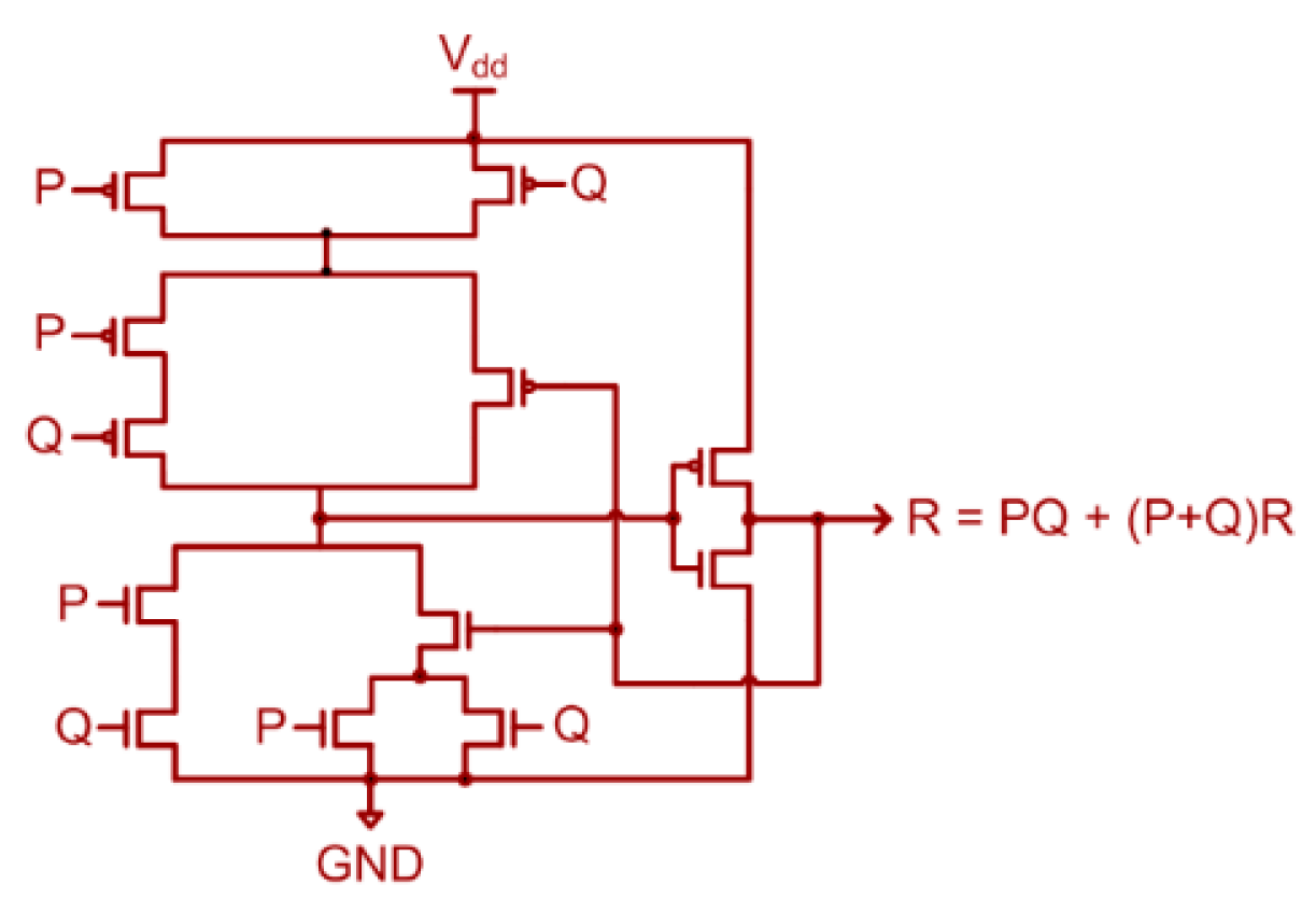
The C-element is a rendezvous element that is often used to construct asynchronous circuits. If all the inputs to a C-element are 1 or 0, it would output 1 or 0, respectively. On the other hand, if any of the inputs to a C-element is different, the C-element would retain its existing steady state. A static CMOS realization of a 2-input C-element [
12] is shown in
Figure 2, where P and Q are the inputs and R is the output. In
Figure 1b,c, the circles with the marking ‘C’ represent the C-element.
AIN and AOUT represent acknowledgment input and output control signals in
Figure 1, which are Boolean complements of each other. AIN and AOUT are used for data communication, i.e., for handshaking between the input and output register banks, and they control the data flow in an input-output mode asynchronous pipeline stage. Dual-rail encoding of inputs and outputs is performed according to the handshake scheme used. For example, a signal A is encoded into dual-rail signals (A
1,A
0) based on RTZH and RTOH, as shown in
Table 1.
In
Table 1, with respect to RTZH [
11], A
1 = 1 and A
0 = 0, and A
0 = 1 and A
1 = 0 are referred to as
data. Only one of the rails of each dual-rail encoded input is asserted high to represent data, and binary 1 is used to represent data in the case of RTZH. A
1 = A
0 = 0 is referred to as the
spacer that is supplied between two data inputs, and A
1 = A
0 = 1 is designated as indeterminate or illegal.
With respect to RTOH [
13], A
1 = 0 and A
0 = 1, and A
0 = 0 and A
1 = 1 are referred to as
data. Only one of the rails of each dual-rail encoded input is asserted low to represent data, and binary 0 is used to represent data in the case of RTOH. A
1 = A
0 = 1 is referred to as the
spacer that is supplied between two data inputs, and A
1 = A
0 = 0 is deemed indeterminate.
Four phases or steps are involved in RTZH and RTOH. In the case of RTZH, with AIN being 1 initially, a fresh data can be input to the asynchronous circuit for processing, and after this, AOUT would assume 1 through the completion detector. Subsequently, AIN would assume 0. With AIN = 0, the spacer is supplied to the asynchronous circuit for processing, and eventually AOUT will assume 0 through the completion detector and AIN would assume 1 again. Another data sequence can then be input to the asynchronous circuit for processing. These imply that the application of inputs according to RTZH follows the sequence data-spacer-data-spacer and so on, i.e., the data bus would entirely assume zero after the application of an input data.
In the case of RTOH, with AIN being 1 initially, the spacer is supplied to the asynchronous circuit for processing, and AOUT would assume 1 through the completion detector. Following this, AIN would assume 0, and a fresh data can be input to the asynchronous circuit for processing. Subsequently, AOUT would assume 0, implying that AIN will assume 1 again and the spacer can be supplied. These imply that, according to RTOH, the application of inputs follows the sequence spacer-data-spacer-data and so on, i.e., the data bus entirely assumes one after the application of an input data.
Example completion detectors corresponding to RTZH and RTOH are shown in
Figure 1b,c, respectively, assuming that single rail primary inputs A and B are dual-rail encoded as (A
1,A
0) and (B
1,B
0). The dual rails of each encoded primary input is combined using a two-input OR gate in the case of RTZH and a two-input AND gate in the case of RTOH. The outputs of two-input OR (AND) gates are combined using a C-element in the case of RTZH (RTOH) to produce the completion detector output. When many two-input OR gates or two-input AND gates are present, their outputs can be combined using a tree of C-elements to produce the completion detector output. The output of the completion detector acknowledges the receipt of all the primary inputs given to the asynchronous circuit for processing.
3. Proposed Early Output Majority Voter and Asynchronous TMR Implementation
The block diagram of an asynchronous TMR implementation is shown in
Figure 3, with asynchronous function blocks 1, 2 and 3 all being identical. Dual-rail encoding is used and four-phase RTZH or RTOH may be used. At least two out of the three function blocks should always maintain the correct operation. In
Figure 3, (A
1,A
0), (B
1,B
0) and (C
1,C
0) represent the dual-rail primary inputs given to asynchronous function blocks 1, 2 and 3, and (X
1,X
0), (Y
1,Y
0) and (Z
1,Z
0) are their corresponding primary outputs which are majority voted to generate the voter’s primary output (M
1,M
0).
The logic expressions of the majority voter outputs corresponding to RTZH are given by Equations (1) and (2), where the first three terms on the right side of the equations signify the correct operation of at least two function blocks and the last term specifies the correct operation of all the function blocks.
The logic expressions of the majority voter outputs corresponding to RTOH are given by Equations (3) and (4). In general, the dual of the logic expressions corresponding to RTZH would give rise to logic expressions that adhere to RTOH, and vice-versa. It may be recalled that binary 1 is used to represent data in the case of RTZH with zeroes used as the spacer and binary 0 is used to represent data in the case of RTOH with ones used as the spacer.
The truth table of the dual-rail encoded majority voter corresponding to RTZH and RTOH is given in
Table 2.
The proposed early output majority voter is shown in
Figure 4, where
Figure 4a corresponds to RTZH and
Figure 4b corresponds to RTOH. To transform a circuit that corresponds to RTZH into one that corresponds to RTOH and vice versa, excepting the C-elements, the rest of the gates should be replaced by their respective duals. This property was proven through induction in [
14].
Figure 4a comprises two complex gates and
Figure 4b also comprises two complex gates. An AO222 or an OA222 complex gate is realized in static CMOS style using 12 transistors. Hence,
Figure 4a,b would require just 24 transistors each for a static CMOS implementation.
Figure 4a,b perhaps represent the ultimate gate-level design of an early output asynchronous majority voter based on dual-rail encoding which correspond to RTZH and RTOH respectively. This is because
Figure 4a,b feature only one gate for each rail of the encoded voter output.
The proposed early output majority voter is a monotonic Boolean network (MBN) [
15]. Referring to
Figure 3, the asynchronous TMR implementation consisting of identical function blocks and the proposed majority voter(s) is also an MBN. In an MBN, the signal transitions monotonically increase or decrease from the primary inputs up to the primary outputs subsequent to the application of inputs [
16]. In an MBN corresponding to RTZH, the signal transitions monotonically increase from binary 0 to 1 for the application of data, and monotonically decrease from binary 1 to 0 for the application of spacer. For example, after the application of spacer in
Figure 4a, if data are applied whereby X
0, Y
0 and Z
0 assume 1, then M
0 would assume 1. Subsequently, in the following return-to-zero phase, if X
0, Y
0 and Z
0 assume 0, M
0 would also assume 0.
On the other hand, in an MBN corresponding to RTOH, the signal transitions monotonically decrease from binary 1 to 0 for the application of data, and monotonically increase from binary 0 to 1 for the application of spacer. For example, after the application of spacer in
Figure 4b, if data are applied whereby X
0, Y
0 and Z
0 assume 0, then M
0 would assume 0. Subsequently, in the following return-to-one phase, if X
0, Y
0 and Z
0 assume 1, M
0 would also assume 1.
An early output asynchronous circuit [
17] is able to commence the processing after receiving just a subset of the primary inputs and can produce all the primary output(s). The early output nature of the proposed majority voter shown in
Figure 4a is described by an example scenario as follows. After the application of data, X
1 = Y
1 = 1 could result in M
1 = 1 early in accordance with the Boolean majority, regardless of Z
1 having assumed 1. Subsequently, in the following return-to-zero phase after the application of spacer, if X
1 and Y
1 assume 0, M
1 could assume 0 early regardless of Z
1 or Z
0 having assumed 0. Thus, the early output nature may be manifested for the application of data and/or spacer in
Figure 4a.
The early output nature of the proposed majority voter shown in
Figure 4b is described by an example scenario as follows. With M
1 and M
0 being 1 initially (due to the application of spacer), if X
1 and Y
1 assume 0 after the application of data, M
1 could assume 0 early regardless of Z
1 having assumed 0. Subsequently, in the following return-to-one phase, if X
1 and Y
1 assume 1, M
1 could assume 1 early, regardless of Z
1 having assumed 1. Thus, the early output nature may be manifested for the application of data and/or spacer in
Figure 4b.
The proposed early output majority voter is different from the majority voters presented in [
8,
9], which are strongly indicating. A strongly indicating asynchronous circuit [
18] requires all the primary inputs to process and produce all the primary output(s). This implies that a strong indication majority voter would require all the primary inputs to process them and produce data as well as spacer. Due to this strict timing constraint, strong indication asynchronous circuits generally have inferior design metrics compared to other categories of asynchronous circuits [
14]. Although the majority voter presented in [
10] is of early output type, similar to our proposed majority voter, however, it contains relatively more logic and hence our proposed majority voter facilitates better optimization of the design metrics, which is discussed in the next section.
4. Results
TMR circuits incorporating existing majority voters [
8,
9,
10] and the proposed majority voter called “NEO_MV” were implemented adhering to RTZH and RTOH, separately. A full adder [
19] was used to represent the function blocks. Excepting the 2-input C-element that was custom realized, as shown in
Figure 2, the rest of the gates were directly utilized from the 32/28 nm CMOS standard digital cell library [
20]. A typical case process, voltage and temperature specification corresponding to a low leakage (high V
t) process with a supply voltage of 1.05V and an operating junction temperature of 25 °C was considered for the simulations. Default wire loads were included, and a fan-out of 4 drive strength was assigned to all the output ports, i.e., majority voter outputs.
Different TMR implementations were simulated, and their functionality was verified by considering all the distinct inputs for the function blocks, which were supplied through a test bench. The test bench indirectly modelled the presence and absence of fault(s) in the function block(s). In other words, all the distinct combinations of the majority voter’s primary inputs shown in
Table 2 were generated through the outputs of function blocks to perform functional simulations of the majority voters. For example, referring to
Table 2, with respect to RTZH, X
1 = Y
1 = Z
1 = 1 and X
0 = Y
0 = Z
0 = 1 denote those instances when all the function blocks operate correctly and produce the same outputs. The remaining instances represent the scenarios when one of the function blocks is faulty, but a majority of the function blocks still operate correctly. Likewise, with respect to RTOH, referring to
Table 2, X
1 = Y
1 = Z
1 = 0 and X
0 = Y
0 = Z
0 = 0 refer to those instances when all the function blocks operate correctly and produce the same outputs. The remaining instances represent the scenarios when one of the function blocks is faulty. However, a majority of the function blocks still operate correctly. The test bench was supplied at a latency of 2 ns, i.e., at a cycle time of 4 ns. The switching activity data obtained from the simulations were used to estimate the total power dissipation.
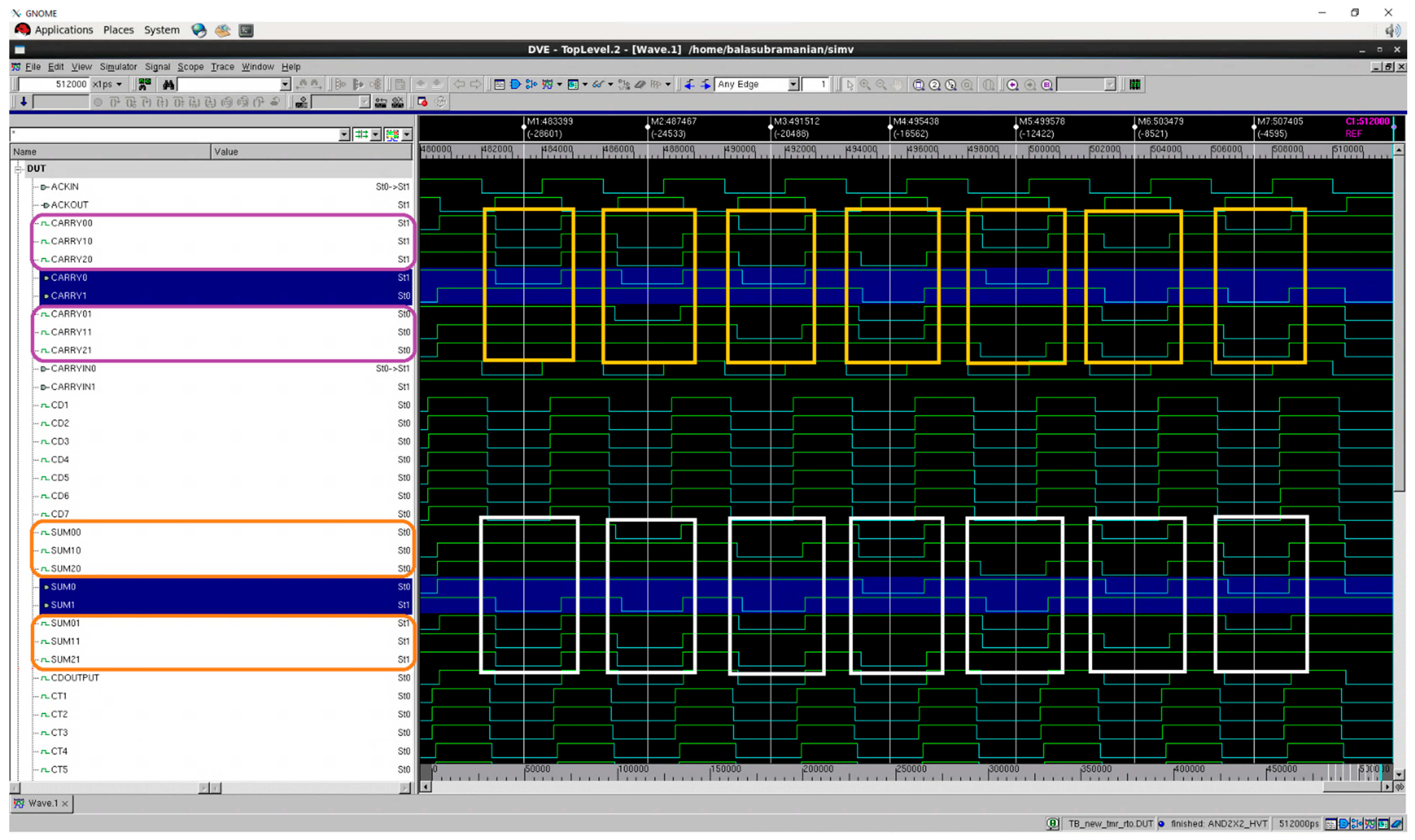
Screenshots of portions of simulation waveforms of TMR implementations utilizing the proposed majority voter (NEO_MV) are shown in
Figure 5 and
Figure 6, corresponding to RTZH and RTOH, respectively. In
Figure 5 and
Figure 6, (SUM21,SUM20), (SUM11,SUM10) and (SUM01,SUM00) represent the sum outputs of triplicated full adders while (CARRY21,CARRY20), (CARRY11,CARRY10) and (CARRY01,CARRY00) represent the carry outputs of the full adders. The majority voted sum and carry outputs are denoted by (SUM1,SUM0) and (CARRY1,CARRY0) in
Figure 5 and
Figure 6, whose waveforms are highlighted in blue. The waveforms in
Figure 5 and
Figure 6 show that correct majority voted outputs are produced in accordance with the Boolean majority despite the faulty behavior of a function block.
In an input-output mode asynchronous circuit, the cycle time is an important metric that governs the operating speed. The cycle time is the time duration to complete one transaction that involves the processing of a data and the spacer. The time taken to process the data and the spacer are called forward latency and reverse latency respectively, and the cycle time is the sum of these latencies. For the TMR implementations considered, their forward and reverse latencies are equal, and so the cycle time is equal to a doubling of the forward latency/reverse latency.
The standard design metrics such as area, cycle time, and power dissipation were estimated for different TMR implementations corresponding to RTZH and RTOH, and they are given in
Table 3. The differences in the design metrics of TMR implementations are entirely attributable to the differences in the logic of the majority voters, since the function blocks, registers and completion detector used are the same.
Overall, from
Table 3, we see that the proposed NEO_MV enables better reductions in area, cycle time, and power dissipation compared to its counterparts. This is due to two main reasons. Considering both RTZH and RTOH, on average, the areas of the majority voters are found as: Singh_MV–50.57µm
2; DIMS_MV–45.75 µm
2; Toms_MV–43.20 µm
2; SI_MV–37.11 µm
2; CG_MV–25.92 µm
2; EO_MV–17.79 µm
2; and the proposed NEO_MV–6.61 µm
2. Therefore, NEO_MV requires 62.8% less area compared to the best of the existing majority voters viz. EO_MV. The lesser area occupancy of NEO_MV leads to lesser power dissipation, and its latency is less because it has a single logic level. The split-up of power dissipated by majority voters and the power dissipated by function blocks, registers and completion detector is also given in
Table 3. The sum of these power components gives the total power dissipation. From
Table 3, we note that compared to EO_MV, NEO_MV dissipates 36.8% less power for RTZH and 37.2% less power for RTOH, i.e., 37% less power on average. Overall, NEO_MV enables reduced total power dissipation for the TMR implementations comprising it compared to TMR implementations incorporating the other majority voters.
Besides estimating the standard design metrics such as cycle time, area and average power dissipation, some figure-of-merits (FOMs) are also calculated for VLSI designs. It is desirable to have reduced design metrics which is characteristic of an effective circuit design. Given this, the FOMs are a combined interpretation of the design metrics. Some popular FOMs include area–delay product (here, area–cycle time product (ACTP)), power-delay product (here, power–cycle time product (PCTP)), and area–delay–power product (here, area–cycle time–power product (ACTPP)). Among these, PCTP is representative of energy.
We calculated the actual values of the above mentioned FOMs for all the TMR implementations and then normalized them. To normalize, the highest value of actual FOM of a TMR implementation with respect to a specific handshake scheme was considered as the baseline and this was used to divide the actual FOM of all the TMR implementations. This procedure was followed to normalize the FOMs of various TMR implementations corresponding to RTZH and RTOH separately, and the normalized FOMs are portrayed by
Figure 7a,b. A smaller value is preferable for a normalized FOM, which is indicative of an effective circuit design.
In
Figure 7a, the blue, orange and grey bars denote normalized ACTP, PCTP and ACTPP, respectively, corresponding to RTZH, and in
Figure 7b, the orange, yellow and green bars denote the same order of normalized FOMs with respect to RTOH. It is clear from
Figure 7a,b that TMR implementations utilizing the proposed majority voter (NEO_MV) achieve better optimized FOMs compared to TMR implementations incorporating the other majority voters. This is due to the reduced design metrics reported for NEO_MV compared to its counterparts, as noted from
Table 3.
From
Figure 7a,b, and
Table 3, it may be inferred that among the existing majority voters, EO_MV is optimized. However, the proposed NEO_MV is better optimized than EO_MV. TMR implementations incorporating NEO_MV achieve the following savings in FOMs compared to TMR implementations incorporating EO_MV: (i) 10.7% reduction in ACTP, 4.1% reduction in PCTP (energy) and 12.5% reduction in ACTPP with respect to RTZH; and (ii) 12.7% reduction in ACTP, 6.9% reduction in PCTP (energy) and 14.9% reduction in ACTPP with respect to RTOH.


