Article

Study on Multiple Input Asymmetric Boost Converters with Simultaneous and Sequential Triggering

by
Juan-Gerardo Parada-Salado
1,
Martín-Antonio Rodríguez-Licea
2,*,
Allan-Giovanni Soriano-Sanchez
2,
Omar-Fernando Ruíz-Martínez
3,
Alejandro Espinosa-Calderon
4 and
Francisco-Javier Pérez-Pinal
1
1
Departamento de Electrónica, Tecnológico Nacional de México en Celaya, Antonio García Cubas 600, Celaya 38010, Mexico
2
Laboratorio de Investigación en Electrónica Aplicada, CONACYT-Tecnológico Nacional de México en Celaya, Antonio García Cubas 600, Celaya 38010, Mexico
3
Faculty of Engineering, Universidad Panamericana, Josemaria Escriva de Balaguer 101, Aguascalientes 20290, Mexico
4
Centro Regional de Optimización y Desarrollo de Equipo de Celaya, Diego Arenas Guzmán 901, Celaya 38023, Mexico
*
Author to whom correspondence should be addressed.
Electronics 2021, 10(12), 1421; https://doi.org/10.3390/electronics10121421
Submission received: 29 May 2021 / Revised: 10 June 2021 / Accepted: 10 June 2021 / Published: 13 June 2021
(This article belongs to the Section Power Electronics)

Abstract

:
Paralleled boost asymmetric configurations operating in discontinuous conduction mode (DCM) are suitable for integrating dissimilar green energy generating sources and control algorithms in versatile scenarios where voltage step-up, low cost, stable operation, low output ripple, uncomplicated design, and acceptable efficiency are needed. Unfortunately, research has mainly been conducted on the buck, sepic, switched-capacitor, among other asymmetric configurations operating in continuous conduction mode (CCM), to the authors’ knowledge. For asymmetric boost type topologies, achieving simultaneous CCM is not a trivial task, and other problems such as circulating currents arise. Research for interleaved converters cannot be easily extended to asymmetric boost topologies due to the dissimilarity of control algorithms and types of sources and parallel stages. This paper analytically establishes properties of stability, output ripple, output voltage, and design for asymmetrical paralleled boost converters operating in DCM with simultaneous or phase delayed (sequential) triggering. A 300 W experimental design and the respective tests allow validation of such properties, resulting in an easy-to-implement configuration with acceptable efficiency.

1. Introduction

Wind generators, photovoltaic modules (PVM), fuel cells (FC), storage systems (batteries), and many other energy sources should be integrated into green power distributed generation plants (hybrid sources) [1,2,3,4] and modern smart grids [5,6,7,8]. If any energy sources cannot provide energy, the rest could satisfy the customers’ energy demand as a multiple uninterrupted power supply.
Smart grids require higher voltage levels (enough to convert to 120/220 VAC) than those provided by energy sources such as PVM or FC. For example, outstanding research was aimed to obtain very high gain and efficiency levels for a single source by combining switched-capacitor and sepic stages [9] or new interleaved boost configurations [10]. Several investigations on interleaved-type converters proposed models and control schemes based on phase-shifted triggering for multiple stages and a single source; these would allow for a power increase, decrease input and output distortions (ripple), and even mitigate nonlinear bifurcation phenomena [11,12,13,14,15,16,17,18].
However, the integration of several different energy sources by power electronic converters (PEC) is necessary but presents complications (recirculating currents, harmonics, high ripple, degradation phenomena, among others) to match the grid impedance, mainly due to the dissimilarity in power capacities. Even the series interconnection of several power sources of the same type creates undesirable effects—for instance, the well-known potential-induced degradation of PVM due to their series interconnection [19].
Parallel multiple input PEC with boost stages operating in DCM are still promising configurations for a scenario of hybrid sources combining MPPT with other algorithms due to their simplicity, low cost, and acceptable efficiency for high voltage gains. CCM implies high-capacity, costly, and voluminous inductors and cannot be ensured for all power-demand regimes [20]. In discontinuous conduction mode (DCM), the converter efficiency is always higher than in CCM [21,22]. Unfortunately, most research on asymmetric paralleled topologies has been devoted to more complicated configurations, which have a higher cost or a low gain, such as sepic, buck-boost, and their variants and combinations operating in CCM, or consider few inputs, among other disadvantages [23].
In [24], the authors analyzed two buck, boost, and buck-boost paralleled, and asymmetrical stages operating in CCM; ripple and output voltage estimations were presented, and a small-signal model was developed to design an output voltage controller by an average current-mode approach. Unfortunately, for green energy sources, Maximum Power Point Tracking (MPPT) controllers are regularly used for more than two stages. The authors in [25,26] proposed single-inductor converters with n inputs and m outputs, and a complete analysis of ripple and output voltages; however, since the inputs must be order-connected by their voltage level, this converter is not suitable for hybrid sources requiring MPPT and other algorithms. In [27,28,29,30,31], the authors presented a voltage accumulator with n inputs and a switched diode-capacitor voltage accumulator on conventional boost converters and included steady-state analyzes; however, many capacitors/components decrease reliability, and MPPT is not achieved. The authors in [32] proposed a single-inductor, asymmetric, boost type, two-input converter to operate multiple MPPT via a sequential triggering; although they presented a circuit design methodology, stability was not ensured for combining other control algorithms or power source types. Furthermore, the single inductor must be of considerable capacity, cost, and dimensions, in addition to withstanding high stress in CCM. A paralleled boost asymmetric configuration combined with a buck topology was presented in [33]; although the configuration can be easily extended to n boost stages, the authors do not guarantee the simultaneous and independent operation of the hybrid sources and presented only basic analyzes for CCM.
The authors in [34] presented a parallel multiple-input PEC with boost stages operating in CCM to feed an h-bridge inverter configuration and included a design analysis; although the controllers were independent for all of the PVM, the authors solved the boost-stages equalization problem by integrating two additional MOSFETS per stage to achieve the decoupling, increasing monetary and computational costs and decreasing efficiency. In [35], the authors analyzed the symmetric configuration of boost interleaved and paralleled stages in CCM to combine FC and PVM. Unfortunately, the authors considered equal stages and similar input voltage levels, simplifying the formulations considerably. Neither did they consider combining different algorithms and MPPT, nor was a stability analysis performed; hence, this work cannot be extended to asymmetric configurations. The authors in [36], presented an asymmetric configuration of n boost paralleled stages operating in CCM with simultaneous triggering and equal duty-cycle; the authors only presented a basic formulation for the output voltage. In [37], the authors presented an analysis of two interleaved converters of two stages connected in parallel and with a 180-degree phase-shift for the stages (sequential triggering). Steady-state analysis was provided for operation in CCM. Unfortunately, the study was limited to two power supplies with two inductors and two switches per source; furthermore, the CCM has the same disadvantages as the previous proposals.
Other modified/new architectures for two (hybrid) sources can be consulted in [38,39,40,41,42,43,44], to mention only a few.
Some interesting adverse effects of uncontrolled and arbitrary phase-delay triggering in paralleled stages with a final diode (as the case of boost topologies), were numerically shown in [45]; however, the benefit of a sequential triggering over the input/output current ripple reduction is well known [46,47]. Regardless of the above, no analytical research has been conducted on the benefits of a sequential triggering (with phase delay instead simultaneous) for paralleled boost converters operating in DCM for n stages and controllers, to the authors’ knowledge. Neither was any study found on the combination of MPPT algorithms for some sources, with other control strategies for different sources, for boost paralleled converters.
Hence, from the review above, the found research cannot be easily extended or modified to the design of multiple-input converters, with n asymmetric boost stages, operating in DCM and sequential or simultaneous triggering. This paper presents the following contributions:
  • An output voltage stability analysis for an n paralleled boost stages converter operation with MPPT control combined with other controllers.
  • Formulations for the steady-state voltage gain and the output voltage ripple.
  • An approach to design an easy-to-implement, versatile, and stable boost-type paralleled MIC with n unequal stages and sources and independent controllers (MPPT/other). This strategy allows different energy sources to feed a resistive load and decouple the paralleled boost stages without extra components, avoiding circulating currents with a low-cost implementation. The output voltage and current ripples are diminished in comparison with simultaneous triggering schemes; an experimental exemplification of the MIC design is provided.
With these objectives in mind, this document is organized as follows. Section 2 presents the MIC setup and dynamic modeling from a switched-systems perspective. The analysis ensures stability regardless of whether multiple MPPT controllers are combined with other strategies. In Section 3, the steady-state analysis to determine the averaged and ripple output voltage levels for sequential triggering are presented, and the ripple concerning simultaneous triggering is compared. Section 4 is aimed at the design of the MIC and the experimental platform. Section 5 and Section 6 present numerical and experimental validations of the models and, finally, Section 7 is dedicated to providing some discussion, conclusions, and future work.

2. Paralleled-Boost-Converter, Dynamic Modeling, and Stability

Let us begin by recalling the boost converter large-signal analysis, which is regularly used in the literature [20,48,49]. This analysis can be extended to n asymmetric boost stages connected in parallel to study the MIC configuration shown in Figure 1a. For sequential or phase-delayed triggering, the activations of MOSFETs/switches are ordered and evenly distributed within every operation period T s , of a pulse width modulator (PWM). To be precise, sequential triggering means that the Q i -th MOSFET is deactivated (off-state) T s / n seconds after the Q i 1 switch was deactivated, and the first MOSFET is deactivated T s / n seconds after the n-th MOSFET (n is the number of stages); activation-timing must be calculated on this time base (see Figure 1b) with u i , 1 1 / n where u i , 1 is the duty-cycle of the i-th stage. Only a single switch is activated at a time, and the next switch is activated when the previous has been deactivated; this allows simultaneous energy charge of inductors to be avoided. On the other hand, while the first switch is deactivated, the stored energy flows towards the load until it is discharged. Within this period, two scenarios are possible: another single switch can be activated to charge the next inductor, or all switches remain deactivated until another switch should be activated. In other words, for the sequential triggering proposed in this paper, the simultaneous charge of two or more inductors is not allowed, nor is the simultaneous discharge of two or more inductors allowed; this is because additional harmonics are introduced (currents through the diodes are summed within T S / n , and the ripple stops having a triangular shape).
Table 1 illustrates the allowed operation modes of the MIC with two stages, including their corresponding dynamic equations; note that the quantity of modes depends on the number of stages, but only subindexes in equations change and can be easily extended to n > 2 . The gray lines in the schematics indicate no current flow, while black lines mean a current flow. Figure 2 shows an exemplification of the sequential triggering for the two stages MIC and the obtained mode sequence. Note that such a sequence depends on the duty cycles, but simultaneous charge and discharge of inductors are avoided.
From a switched-systems perspective, considering that the duty cycle for any stage is 0 D i < 1 / n where i = 1 , 2 , . . . , n and differentiating the voltage equations in each mode (one looks only for the output voltage dynamic behavior), one can get the following switched system (arbitrary switching) from Table 1 equations:
x ˙ = A i x + B i
where x = x 1 , x 2 T = V o , V ˙ o , i = 1 , 2 , . . . , n + 1 , and
A 1 = 0 1 1 L 1 C 1 R C , A 2 = 0 1 1 L 2 C 1 R C , . . . , A n = 0 1 1 L n C 1 R C , A n + 1 = 0 1 0 1 R C , B 1 = 0 e 1 L 1 C , B 2 = 0 e 2 L 2 C , . . . , B n = 0 e n L n C , B n + 1 = 0 0 .
Since the dynamic (qualitative) behavior of each autonomous subsystem is invariant to shifts in the equilibrium point [50], one can propose n coordinate changes y = x x e where x e is the respective equilibrium point (abusing notation):
y ˙ = A i y
where
A 1 = 0 1 ρ L 1 C 1 R C , A 2 = 0 1 ρ L 2 C 1 R C , . . . , A n = 0 1 ρ L n C 1 R C ,
and ρ { 0 , 1 } is introduced to consider the last ( A n + 1 ) subsystem (for simplicity in the next algebra).
In the following, a stability test is developed under a common Lyapunov function (CLF) design approach. Hence, stability is ensured despite arbitrary switching [51] regardless of the control actions of n MPPT control systems or of the combination of MPPT control for some stages, and other controllers for the rest.
Consider the common Lyapunov candidate function:
V ( y ) = y T P y , P = 1 p 2 p 2 p 3
where p 2 , p 3 R must be constants such that P 0 (positive definite); note that V ( y ) = 0 in y = [ 0 , 0 ] T . Since one looks for P 0 , the leading minors of P must be positive, hence d e t ( P ) > 0 (Sylvester’s criterion) such that p 3 > p 2 2 is the first condition to meet.
The time derivative of V ( y ) along the system trajectories is:
V ˙ = y T ( P A i + A i T P ) y
In order to ensure stability despite the arbitrary switching, Q i = P A i + A i T P 0 (negative definite) for all i, and for all ρ { 0 , 1 } . Consider the case ρ = 1 , the principal minors of Q i are as follows:
M 1 = 2 p 2 L i C
M 2 = L i 2 C 2 R 2 2 L i 2 R C p 2 + 4 L i C R 2 p 2 2 2 L i C R 2 p 3 2 + L i 2 p 2 2 2 L i R p 2 p 3 L i 2 C 2 R 2 R 2 p 3 2 L i 2 C 2 R 2
Q i 0 if M 1 < 0 hence, p 2 > 0 is a second condition to meet (odd leading minors must be less than zero). Besides, it must also be fulfilled that M 2 > 0 :
L i 2 C 2 R 2 + 2 L i 2 R C p 2 ( 4 L i C R 2 + L i 2 ) p 2 2 + 2 L i R p 2 p 3 + 2 L i C R 2 p 3 R 2 p 3 2 > 0
This is to say, the even minor must be greater than zero. Selecting the worst-case values (for the previous inequality) of L m L i L M , where L m is the lowest L i value and L M is the highest L i value, p 2 and p 3 values should be selected such that
L m 2 C 2 R 2 + 2 L M 2 R C p 2 ( 4 L m C R 2 + L m 2 ) p 2 2 + 2 L M R p 2 p 3 + 2 L m M C R 2 p 3 R 2 p 3 2 > L i 2 C 2 R 2 + 2 L i 2 R C p 2 ( 4 L i C R 2 + L i 2 ) p 2 2 + 2 L i R p 2 p 3 + 2 L i C R 2 p 3 R 2 p 3 2 > 0
Selecting
p 2 = 2 L M 2 R C 4 L m R 2 C + L m 2 > 0
the second condition is met, and the inequality (8) reduces to
L m 2 C 2 R 2 + 2 L M R p 2 p 3 + 2 L m M C R 2 p 3 R 2 p 3 2 > 0
Setting
p 3 = 2 L M p 2 + 2 L M C R 2 R > 0
Inequality (10) reduces to
p 2 > 0 > R C L m L M L M
such that the second condition is congruent. Now, it must be proved that p 3 > p 2 2 , which is the first previously stated condition; substituting p 3 from (11) in such inequality one has:
L M p 2 + L M C R > 2 p 2 2
and it is enough to demonstrate that the sole first term is greater than the right side of the previous inequality when p 2 from (9) is used:
L M p 2 > 2 p 2 2
4 L M R 2 C + L M 2 > 4 L m R 2 C + L m 2 > 4 L M R 2 C
L M 2 > 0
Consider now the case ρ = 0 and note that ρ 0 when L i i , such that the previous analysis for M 2 holds. On the other hand, it is easy to demonstrate that M 1 0 when L i , hence Q i is negative semi-definite. In other words, the bounding of the solutions or practical stability (or simply ’stability’) can be ensured; in fact, since there will always be a ripple in the output voltage due to switching between modes, asymptotic stability cannot be expected, but rather the confinement of the system solutions to a small region of the state space. Such regions, in this case, correspond to the level of the ripple of the output voltage that will be estimated in the next section.

3. Steady-State Analysis

In the previous section, a dynamic analysis of the MIC was done regardless of the triggering. Next, the output voltage level and the voltage ripple will be obtained by steady-state analysis for the multiple-input, sequential triggering converter (MISeC), and, for completeness purposes, also with simultaneous triggering (MISiC) for comparison purposes.

3.1. Averaged Output Voltage for the MISeC

Considering the MISeC with n parallel boost stages and ideal components, each inductor current will increase linearly when the corresponding MOSFET is activated (on-state), as illustrated in Figure 1b. If the MOSFET is turned off, the corresponding inductor current decreases linearly to zero. Note that the corresponding diode prevents a reverse current through such an inductor; hence the current remains zero (DCM) until the next period ( T s ) is started, as illustrated in Figure 3a. The sequential triggering can grant an energy flow toward the load with independent control for each stage, ensuring that the average current < i D , o u t > can be calculated as follows:
< i D , o u t > = 1 T s 0 T s i D 1 + i D 2 + . . . + i D n d t
where i D i is the corresponding current through the diode for each stage.
To calculate i D i , the graphic depicted in Figure 3b shows the behavior of the current through the diode within a T s period, and whose value can be calculated using the triangle area formulation:
i D i = T s 2 ( I p k i u i , 2 ) .
Substituting (18) in (17) one has:
0 T s i D , o u t = T s 2 I p k 1 u 1 , 2 + I p k 2 u 2 , 2 + . . . + I p k n u n , 2
where u i , 2 is the i-th inductor discharge period, and I p k i represents the respective inductor peak current (see Figure 3). I p k i can be calculated as [52]:
I p k i = e i L i u i , 1 T s .
Substituting (20) in (19), the average current of all of the diodes can be approximated by:
< i D , o u t > = T s 2 i = 1 n 1 e i u i , 1 u i , 2 L i .
The discharge period u i , 2 can be calculated by the relationship between the legs and the hypotenuse derived from the current’s triangular shape through the diode, as shown in Figure 3b. This means that the tangent angle is a function of u i , 2 , and I p k i , and its value can be expressed as follows:
( e i V o ) L i = I p k i u i , 2 T s .
Solving for u i , 2 one has:
u i , 2 = e i u i , 1 V o e i .
Note that in the previous equations, the notation for V o is being abused because it was also used in the switched model, and it should not cause confusion since it now represents the same voltage but is seen in an averaged way.
Substituting u i , 2 from the preceding expression into Equation (21) and considering that the maximum current through the diodes is i D , o u t , m a x = V o R , the average output voltage can be expressed as follows:
K 0 V o n + 1 ( e 1 + , . . . , + e n ) V o n + , . . . , + m = 1 n e m V o + , . . . , + m = 1 n e m L m e 1 e 2 L 1 L 2 ( K 1 e 2 L 2 + K 2 e 1 L 1 ) + , . . . , + K n m = 1 n 1 e m L m = 0 ,
where
K 0 = 2 m = 1 n L m R T s , K 1 = e 1 2 u 1 , 1 2 , K 2 = e 2 2 u 2 , 1 2 , . . . , K n = e n 2 u n , 1 2
Equation (24) is a polynomial function where the roots are V o values. One can infer that the real V o value must be the maximum, real and positive one. In later sections, this assumption is validated.

3.2. Output Voltage Ripple for the MISeC

The voltage ripple ( Δ V r i p p l e ) is defined as the difference between the maximum and minimum of the steady-state output voltage, as illustrated in Figure 3c; in this paper, this difference is expressed as a function of the capacitor current as depicted in Figure 3d:
I c = C d V r i p p l e d t = d Q d t
where Q is the capacitor charge. The differential of charge for each stage ( d Q i ) can be approximated using the capacitor charge period u i , 2 , and the triangle area formulation (see Figure 3d):
d Q i = b i h i 2
where h i = I p k i i o is the triangle height, i o the output current, and b i the base width. Using similarity theorems, one has:
b i = ( I p k i i o ) u i , 2 T s I p k i .
To determine the value of b i as a u i , 1 function, one can substitute (23) in (27), thus:
b i = ( I p k i i o ) u i , 1 e i T s I p k i ( V o e i ) .
Substituting the value of u i , 2 in Equation (23), and substituting Equation (27) in (26):
d Q i = 1 2 ( I p k i i o ) 2 u i , 1 e i T s I p k i ( V o e i ) .
Replacing (29) in (25) and solving for the i-th d V r i p p l e :
Δ V r i p p l e , i = ( e i u i , 1 T s ) 2 C I p k i ( I p k i i o ) 2 V o e i .
Using L i from Equation (20), Equation (30) can be expressed as:
Δ V r i p p l e , i = L i 2 C ( I p k i i o ) 2 V o e i .
Since one looks only for the maximum ripple:
Δ V r i p p l e = m a x i L i 2 C ( I p k i i o ) 2 V o e i .
Usually, keeping a lower percentage of voltage ripple is desirable in converter applications. If the output voltage ripple is greater than that supported by the load, it could be damaged. In the following, the output ripple for the MISiC is calculated; an analytic comparative is performed to show the sequential benefits concerning simultaneous triggering.

3.3. Average Output Voltage for the MISiC

In this scenario, the average current through all of the diodes can be approximated as in Equation (21). Since < I D o u t > = V o / R , the average output voltage can be estimated as:
V o R T s 2 i = 1 n 1 e i u i , 1 u i , 2 L i .
It is important to recall that in this scenario, all of the switches are activated within the same period; this formulation is not precise for the MISeC.

3.4. Output Voltage Ripple for the MISiC

In this scenario, the total peak current I p k due to simultaneous triggering can be calculated as:
I p k = I p k 1 + I p k 2 + I p k 3 + . . . + I p k n .
Considering that the charge interval u i , 1 ends within the same period, the capacitor current can be calculated as in Equation (25). Two scenarios to calculate the area for d Q i are possible. All input/source voltages are the same in the former, and in the latter, all input voltages are different. For the former, substituting Equation (34) in (25) and solving for Δ V r i p p l e , i , one has:
Δ V r i p p l e , i = m a x i ( e i u i , 1 T s ) V o e i ( I p k i o ) 2 2 C I p k .
Note that again, one looks only for the maximum ripple.
For the latter case (different input voltages), and using Figure 4, d Q can be approximated as:
d Q I p k i o 2 u 2 ¯ T s ,
where u 2 ¯ is the average of the discharge periods. Substituting Equation (36) in (25):
Δ V r i p p l e I p k i o 2 C u 2 ¯ T s .
Since u 2 ¯ can be expressed in terms of u i , 1 , (37) can be rewritten as:
Δ V r i p p l e I p k i o 2 C 1 n i = 1 n e i , 1 u i , 1 V o e i , 1 T s .

3.5. Analytic Ripple Comparison for Sequential and Simultaneous Triggering

From Equations (20), (32), and (35), it is easy to see that the ripple for the simultaneous triggering with the same voltage inputs is greater than the sequential case because
I p k = I p k 1 + I p k 2 + I p k 3 + . . . + I p k n > I p k i
for the same duty cycles, except for the trivial case in which all peak currents are zero.
To show that the ripple with simultaneous triggering and unequal voltage inputs is greater than that with sequential triggering, it is enough to compare Equations (20), (32) and (38):
m a x i e i u i , 1 T s 2 C ( V o e i ) ( I p k i i o ) 2 I p k i < I p k 1 + I p k 2 + . . . + I p k n i o 2 C T s 1 n i = 1 n e i , 1 u i , 1 V o e i , 1 ,
m a x i e i u i , 1 ( V o e i ) ( I p k i i o ) 2 I p k i < I p k 1 + I p k 2 + . . . + I p k n i o 1 n i = 1 n e i , 1 u i , 1 V o e i , 1 .
Since the input voltages e i are different:
σ = 1 n i = 1 n e i , 1 u i , 1 V o e i , 1 m a x i e i u i , 1 V o e i < 1 .
Using γ = ( I p k i i o ) / I p k i < 1 :
γ | I p k i i o | < | I p k i i o | < σ | I p k 1 + I p k 2 + . . . + I p k n i o | | I p k 1 + I p k 2 + . . . + I p k n i o | .
Hence,
| I p k i | < | I p k 1 + I p k 2 + . . . + I p k n |
and all of the (rest of the) triangle inequality theorem conditions are met, except, again, for trivial cases in which all or almost all, peak currents are zero.
Section 5 illustrates numerically and graphically how the ripple is considerably less using sequential triggering.

4. Component Selection

The configuration of n parallel stages of the proposed MISeC allows individual component sizing, with the only condition of maintaining the DCM. Considering that the MISeC enables the use of different types of DC sources, a scenario is illustrated and experimented with three 100 W maximum power sources without loss of generality. These sources are two 100 W maximum-power PVM (at 1000 W/m 2 irradiation) and a battery with the capacity to give a constant 100 Wh rate (emulated by a power supply).
For such design, the maximum duty cycle for each stage u m a x , to avoid the superposition of each stage ripple and get a clean (regular) output-voltage signal, is 0 u < 1 / 3 . Here, the PWM operating frequency f s is established as 10 kHz without loss of generality; this frequency is selected here because it is easy to achieve with cheap components such as micro-controllers. Hence, for DCM, the critical inductance is defined as [53,54]:
L c m a x i R u i ( 1 u i ) 2 2 f s
Using an R 10   Ω load, L i < 74 µH, and from Equation (20), a maximum-voltage vs. current trade-off is advertised. Looking for commercial values, Coilcraft inductors of 22 µH and a 35.4 A maximum current are selected because of their availability and low cost. Hence, the peak voltage supported is 23.364 V per stage.
From Figure 5a, the power output and output voltage can be estimated since they depend on the load resistance as stated in the previous sections. The range of power for this design is approximately [ 300 , 600 ] , W and the range of average output voltage is [ 35 , 670 ] V. Here, the load is selected as R = 75   Ω , according to this design. Figure 5b illustrates the output voltage and the voltage ripple as a function of the load resistance for a 25 µF capacitor; hence, this capacitance is selected for the design (this value must be chosen based on the real-application desired ripple level).
Table 2 shows the relevant and real (experimentally measured) parameters obtained from commercial parts. Note that relevant parameters for inductors were individually validated to gain precision on the next validations.

5. Numerical Validation of the Models

To validate the formulations provided, in this section, the results of numerical comparison against PSIM are presented. The previously stated design includes three boost stages, and 22 operation modes are possible. This switched model is integrated into Matlab Simulink, and in both models, the components are considered ideal.
The first validation consists of comparing the output voltage obtained with the proposed model against that provided by PSIM. For this test, e 1 = 17.7 V, e 2 = 17.7 V, and e 3 = 23 (design parameters for maximum irradiation), with 33.3 % duty cycles. In Figure 6, the average and ripple outputs are compared. The PSIM model response is plotted in purple for the averaged output voltage and yellow for the ripple. The model response is plotted in red and blue for the averaged output voltage and ripple, respectively. It can be seen that the average voltage is 157.80 V and 155.92 V, with PSIM and the proposed models, respectively; the voltage ripple is 3.4717 V for the PSIM simulation and 3.3977 V for the proposed model. This is a 0.33 % numerical precision error in average that can be neglected.
Two scenarios for validation for the steady-state formulations are presented. In the former, equal 17.7 V input voltage sources were used, and in the latter e 1 = 12 V, e 2 = 17.3 V, and e 3 = 22 V. In both scenarios, a 33% duty cycle for all stages is used. Other tests with different combinations of input voltage levels and duty cycles were performed, corroborating the model’s validity; however, only representative results are presented.
Figure 7 shows a simulation interval for the first scenario. The upper plot shows the average and ripple output voltages for the MISiC, and the lower for the MISeC, both simulated in Matlab (proposed model) and PSIM. The errors concerning the average voltage for the MISiC formulations are 2.18 and 0.34 % for the proposed model and the PSIM model, respectively; 1.72 and 0.40 % output voltage ripple errors are estimated for the proposed and PSIM models, respectively. For the MISeC formulations, the average voltage errors are 1.53 and 0.35 % for the proposed and PSIM models, respectively; 0.72 and 0.46 % output voltage ripple errors are estimated for the proposed model and the PSIM model, respectively.
The second scenario (different input sources) in Figure 8 shows the average and ripple output voltages for the MISiC in the upper plot, and in the lower plot for the MISeC, both simulated in Matlab (proposed model) and PSIM. The errors concerning the average voltage for the MISiC formulations are 2.10 and 0.39 % for the proposed and PSIM models, respectively; 1.01 and 2.20 % output voltage ripple errors are estimated for the proposed and PSIM models, respectively. For the MISeC formulations, the average voltage errors are 1.57 and 0.35 % for the proposed and PSIM models, respectively; 1.88 and 0.52 % output voltage ripple errors are estimated for the proposed and PSIM models, respectively.
Other tests with different combinations of voltage levels and duty cycles were performed, corroborating the validity of the formulations; however, only representative results are presented here. Note that both the provided model and the formulations for the steady-state output voltage provide reasonable approximations.
For completeness purposes, a comparison of the output voltage ripple (for both MISeC and MISiC) as a function of R is presented. This is, the load resistance varies within a [ 1 , 100 ]   Ω range. Such comparison is plotted in Figure 9. The diminution of the ripple with the MISeC is notable for a wide range of loads, as expected from Section 3.5.

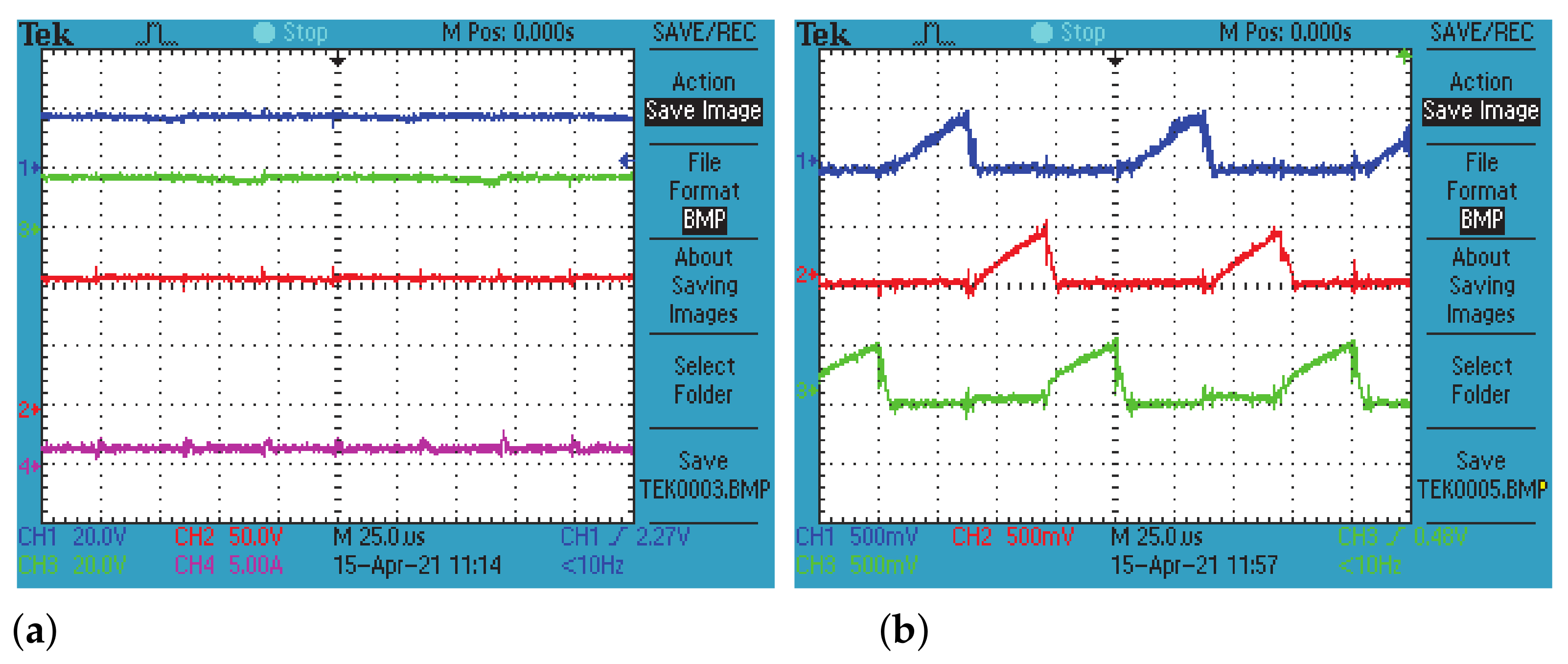
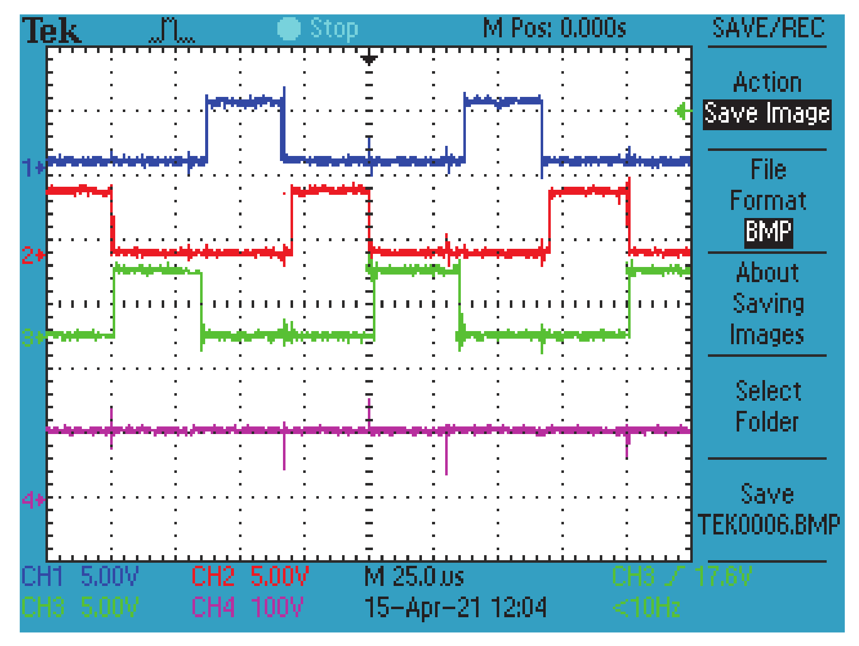
6. Experimental Validation

6.1. Experimental Setup

Figure 10 shows the complete system for the experimental tests, where each photovoltaic module is connected to each of the inputs and the power supply, emulating a battery. The MISeC uses a Microchip DSPIC33, three inline current sensors (at the bottom of the PCB), and other basic circuitry. The DSPIC performs analog to digital conversion, MPPT, and PWM functions. The PCB was built only for prototype test purposes; hence, some noise is expected. A final production PCB design is not the purpose of this paper and is left for future research.

6.2. Controller Design

The following experimental tests are intended to demonstrate that the MISeC allows the independent operation of n MPPT controllers, simultaneously with other power tracking techniques as a constant power rate one—to avoid degradation of fuel cells or batteries, for instance. There are various MPPT algorithms in the literature. Whether by direct methods [55,56,57], or indirect methods [55], it is essential to maintain the maximum power point available. Here, a simple and easy-to-implement technique is used, known as a perturb and observe (P&O) [58,59], illustrated in Figure 11 (for a single MPPT algorithm). This article is not aimed at developing a novel maximum power tracking method. It is important to recall that different MPPT algorithms are calculated individually in the MISeC. Particularly, two independent P&O MPPT algorithms are calculated by the DSPIC33, one for each photovoltaic module stage. The last stage is set to control its output power using a PI controller; this is the case for some fuel cells or batteries in diverse scenarios and is quite different from an MPPT.

6.3. Experimental Tests

Figure 12a shows the PVM voltages, the output voltage, and the output current for high (full) irradiation conditions in both PVMs. Figure 12b shows the currents through the inductors. Note that the charging periods are not simultaneous, and the MPPT algorithms can operate independently from the third stage (constant power). Figure 13 shows the triggering signals and the output voltage for the MISeC. Please refer to Table 3 for efficiency, voltage, power, and current levels.
Figure 14a shows the output voltage ripple with a 5 V/div scale for the MISeC. The average estimated value is 3.40 V, which represents a 2.39 % error with respect to the 3.4834 V calculated with the previously stated formulations. Comparatively, Figure 14b shows the ripple for the MISiC under the same conditions; note that 6.2 V is considerably greater (82%) than for the MISeC. Figure 15 shows the simulations for this previous scenario (the proposed model and PSIM model). It should be mentioned that for this simulation, the values in Table 2 are used, including parasitic resistances. Comparatively, Figure 16 shows the related voltages for the MISiC. Table 4 summarizes the accuracy of the proposed models for this test. The last two columns represent the PSIM model error, and the proposed model error, respectively, both regarding the experimental values. Note that the formulations provide acceptable values.
Finally, two additional experimental tests are presented. For the first one, irradiation is manually depleted on the first photovoltaic module (covered with a translucent film). For the second experiment, the two panels are covered. Figure 17a,b show the triggering pulses and output voltages for such scenarios, respectively. In Figure 18a and Figure 19a, the PVM voltages, the output voltage, and the output current, respectively, are shown for each test. The duty cycle is 25% for a covered panel, while the other remains as in the full irradiation scenario. Figure 18b and Figure 19b show the behavior of the currents through the inductors for each test. Please refer to Table 3 for efficiency, voltage, power, and current levels.
Note that the MISeC allows the independent operation of each MPPT while the ripple is small compared to other configurations and triggering strategies. For completeness purposes, Table 3 resumes power and efficiency values for all the experimental tests. Final production PCB and other considerations will provide better efficiency values; it is not the purpose of this paper to improve the efficiency, but, according to experiments, at least 88% can be obtained. Regardless of the above, the efficiency is much better for the MISeC, with less ripple, and n independent MPPT controllers can be integrated.
From the previous tests, a stable operation of the MISeC can be concluded; multiple MPPT algorithms along with other controllers, such as the constant power one, can be used with acceptable efficiency and low ripple.

7. Discussion, Conclusions, and Future Work

A dynamic model for the boost-type (paralleled) MIC with any finite number of stages/input sources is developed in this paper. Such a model can be used for different control objectives as voltage or current regulation. It is analytically demonstrated that the dynamic model is output-voltage stable for a resistive load regardless of the switching, and hence, of the conduction mode under regular (appropriate) parametrization. The stability in such a sense does not depend on the used controllers, and the controllers can operate independently as long as they follow compatible objectives.
Steady-state analyzes are performed to estimate the average output voltage and the output voltage ripple, including any finite number of stages/input sources. These analyzes can be extended to obtain the ripple of the currents through the inductors, output current ripple, and other variables of interest. Additional study analytically shows that the ripple is considerably reduced regarding a simultaneous triggering in the same electric configuration.
The presented dynamic model, the formulations obtained, the ripple reduction concerning a simultaneous triggering and, the stability under multiple control types (MPPT + constant rate) are validated numerically and experimentally.
The presented configuration allows any finite number of different DC voltage levels to be connected; hence, other energy collectors can be used. PVMs in different locations (irradiation conditions) can be integrated into a single DC bus, avoiding the potential induced degradation (because of their parallel interconnection instead of a series one). Even more, the implementation cost of the MISeC is relatively low.
Future work must consider AC input sources; although rectification could initially solve their integration in the MISeC, new phenomena can be generated, such as power quality issues and resonance effects.

Author Contributions

Conceptualization, M.-A.R.-L. and J.-G.P.-S.; methodology M.-A.R.-L.; software, J.-G.P.-S.; validation, M.-A.R.-L., and J.-G.P.-S.; formal analysis, M.-A.R.-L.; investigation, M.-A.R.-L., J.-G.P.-S., A.-G.S.-S., O.-F.R.-M., A.E.-C., and F.-J.P.-P.; resources, M.-A.R.-L., J.-G.P.-S., and F.-J.P.-P.; writing—original draft preparation, M.-A.R.-L., J.-G.P.-S., A.-G.S.-S., O.-F.R.-M., A.E.-C., and F.-J.P.-P.; writing—review and editing, M.-A.R.-L.; visualization, M.-A.R.-L., J.-G.P.-S.; supervision, M.-A.R.-L.; project administration, M.-A.R.-L.; funding acquisition, M.-A.R.-L., and A.-G.S.-S. All authors have read and agreed to the published version of the manuscript.

Funding

This research was funded by CONACYT grant number Cátedras ID 4155 and 6782, and the scholarship of J.-G.P.-S.

Institutional Review Board Statement

Not applicable.

Informed Consent Statement

Not applicable.

Data Availability Statement

The data that support the findings of this study are available from the corresponding author, M.-A.R.-L., upon reasonable request.

Acknowledgments

Authors would like to thank to the Tecnológico Nacional de México en Celaya for facilitating the use of the Applied Electronics Research Laboratory.

Conflicts of Interest

The authors declare no conflict of interest.

References

  1. Knudsen, T.; Bak, T.; Svenstrup, M. Survey of wind farm control—Power and fatigue optimization. Wind Energy 2015, 18, 1333–1351. [Google Scholar] [CrossRef]
  2. de Alegría, I.M.; Andreu, J.; Martín, J.L.; Ibanez, P.; Villate, J.L.; Camblong, H. Connection requirements for wind farms: A survey on technical requierements and regulation. Renew. Sustain. Energy Rev. 2007, 11, 1858–1872. [Google Scholar] [CrossRef]
  3. Nugent, D.; Sovacool, B.K. Assessing the lifecycle greenhouse gas emissions from solar PV and wind energy: A critical meta-survey. Energy Policy 2014, 65, 229–244. [Google Scholar] [CrossRef]
  4. Cicia, G.; Cembalo, L.; Del Giudice, T.; Palladino, A. Fossil energy versus nuclear, wind, solar and agricultural biomass: Insights from an Italian national survey. Energy Policy 2012, 42, 59–66. [Google Scholar] [CrossRef]
  5. Chen, S.; Zhang, J.; Wang, L.; Zhang, H.; Li, L. Evaluation of Power Quality and Reliability of Distributed Generation in Smart Grid. In Proceedings of the IOP Conference Series: Earth and Environmental Science, Kamakura, Japan, 10–11 October 2020; IOP Publishing: Bristol, UK, 2020; Volume 632, pp. 1–7. [Google Scholar]
  6. Karthikumar, K.; Karthik, K.; Karunanithi, K.; Chandrasekar, P.; Sathyanathan, P.; Prakash, S.V.J. SSA-RBFNN strategy for optimum framework for energy management in Grid-Connected smart grid infrastructure modeling. Mater. Today Proc. 2021. [Google Scholar] [CrossRef]
  7. Anwar, M.; Naeem, A.; Gul, H.; Arif, A.; Fareed, S.; Javaid, N. Electricity Price and Load Forecasting Using Data Analytics in Smart Grid: A Survey. In Proceedings of the International Conference on Emerging Internet, Data & Web Technologies, Kitakyushu, Japan, 24–26 February 2020; pp. 427–439. [Google Scholar]
  8. Al-Badi, A.H.; Ahshan, R.; Hosseinzadeh, N.; Ghorbani, R.; Hossain, E. Survey of Smart Grid Concepts and Technological Demonstrations Worldwide Emphasizing on the Oman Perspective. Appl. Syst. Innov. 2020, 3, 5. [Google Scholar] [CrossRef] [Green Version]
  9. Alishah, R.S.; Yahya Hassani, M.; Hosseini, S.H.; Bertilsson, K.; Babalou, M. Analysis and Design of a New Extendable SEPIC Converter with High Voltage Gain and Reduced Components for Photovoltaic Applications. In Proceedings of the 2019 10th International Power Electronics, Drive Systems and Technologies Conference (PEDSTC), Shiraz, Iran, 12–14 February 2019; pp. 492–497. [Google Scholar] [CrossRef] [Green Version]
  10. Babalou, M.; Dezhbord, M.; Alishah, R.S.; Hossein Hosseini, S. A Soft-Switched Ultra High Gain DC-DC Converter with Reduced Stress voltage on Semiconductors. In Proceedings of the 2019 10th International Power Electronics, Drive Systems and Technologies Conference (PEDSTC), Shiraz, Iran, 12–14 February 2019; pp. 677–682. [Google Scholar] [CrossRef]
  11. Mazumder, S.; Nayfeh, A.H.; Borojevi, C.D. Development of integral-variable-structure control schemes for parallel-buck and parallel-boost DC-DC converters. In Proceedings of the INTELEC. Twenty-Second International Telecommunications Energy Conference (Cat. No. 00CH37131), Phoenix, AZ, USA, 10–14 September 2000; pp. 82–89. [Google Scholar]
  12. Cadirci, I.; Yafavi, A.; Ermiş, M. Unity power factor boost converter with phase shifted parallel IGBT operation for medium power applications. IEE Proc. Electr. Power Appl. 2002, 149, 237–244. [Google Scholar] [CrossRef]
  13. Lee, Y.J.; Emadi, A. Phase shift switching scheme for DC/DC boost converter with switches in parallel. In Proceedings of the 2008 IEEE Vehicle Power and Propulsion Conference, Harbin, China, 3–5 September 2008; pp. 1–6. [Google Scholar]
  14. Neacsu, D.O.; Bonnice, W.; Holmansky, E. On the small-signal modeling of parallel/interleaved buck/boost converters. In Proceedings of the 2010 IEEE International Symposium on Industrial Electronics, Bari, Italy, 4–7 July 2010; pp. 2708–2713. [Google Scholar]
  15. El Fadil, H.; Giri, F.; Guerrero, J.M. Adaptive sliding mode control of interleaved parallel boost converter for fuel cell energy generation system. Math. Comput. Simul. 2013, 91, 193–210. [Google Scholar] [CrossRef] [Green Version]
  16. Cuoghi, S.; Mandrioli, R.; Ntogramatzidis, L.; Gabriele, G. Multileg interleaved buck converter for EV charging: Discrete-time model and direct control design. Energies 2020, 13, 466. [Google Scholar] [CrossRef] [Green Version]
  17. Zhuo, S.; Gaillard, A.; Li, Q.; Ma, R.; Paire, D.; Gao, F. Current Ripple Optimization of Four-Phase Floating Interleaved DC–DC Boost Converter Under Switch Fault. IEEE Trans. Ind. Appl. 2020, 56, 4214–4224. [Google Scholar] [CrossRef]
  18. Ahmed, S.; Kashif, S.A.R.; Ain, N.U.; Rasool, A.; Shahid, M.S.; Padmanaban, S.; Ozsoy, E.; Saqib, M.A. Mitigation of Complex Non-Linear Dynamic Effects in Multiple Output Cascaded DC-DC Converters. IEEE Access 2021, 9, 54602–54612. [Google Scholar] [CrossRef]
  19. Miranda, H.F.B.; da Costa, L.P.; Soares, S.O.; da Silva, J.V. Potential induced degradation (PID): Review. In Proceedings of the 2020 IEEE PES Transmission & Distribution Conference and Exhibition-Latin America (T&D LA), Montevideo, Uruguay, 28 September–2 October 2020; pp. 1–6. [Google Scholar]
  20. Erickson, R.W. Fundamentals of Power Electronics; Springer Science & Business Media: Berlin/Heidelberg, Germany, 2013. [Google Scholar]
  21. Aloisi, W.; Palumbo, G. Efficiency model of boost dc–dc PWM converters. Int. J. Circuit Theory Appl. 2005, 33, 419–432. [Google Scholar] [CrossRef]
  22. Kebaili, S.; Betka, A. Efficiency model of DC/DC PWM converter photovoltaic applications. In Proceedings of the Global Conference on Renewables and Energy Efficiency for Desert Regions, Amman, Jordan, 3–5 April 2018. [Google Scholar]
  23. Hema Chander, A.; Kumar Sahu, L.; Ghosh, S.; Gupta, K.K. Comparative analysis on selection and synthesis of multiple input converters: A review. IET Power Electron. 2020, 13, 611–626. [Google Scholar] [CrossRef]
  24. Kumar, L.; Jain, S. Multiple-input DC/DC converter topology for hybrid energy system. IET Power Electron. 2013, 6, 1483–1501. [Google Scholar] [CrossRef]
  25. Babaei, E.; Abbasi, O. Structure for multi-input multi-output dc–dc boost converter. IET Power Electron. 2016, 9, 9–19. [Google Scholar] [CrossRef]
  26. Lindiya, S.A.; Palani, S.; Vijayarekha, K. Modelling and Simulation of Photovoltaic System Fed Two Input Two Output DC-DC Boost Converter Interfaced with Asymmetric Cascaded H-Bridge Multilevel Inverter. Indian J. Sci. Technol. 2017, 10, 5. [Google Scholar] [CrossRef] [Green Version]
  27. Yuan-mao, Y.; Cheng, K.W.E. Multi-input voltage-summation converter based on switched-capacitor. IET Power Electron. 2013, 6, 1909–1916. [Google Scholar] [CrossRef]
  28. Hou, S.; Chen, J.; Sun, T.; Bi, X. Multi-input step-up converters based on the switched-diode-capacitor voltage accumulator. IEEE Trans. Power Electron. 2015, 31, 381–393. [Google Scholar] [CrossRef]
  29. Varesi, K.; Hosseini, S.H.; Sabahi, M.; Babaei, E. A high-voltage gain nonisolated noncoupled inductor based multi-input DC-DC topology with reduced number of components for renewable energy systems. Int. J. Circuit Theory Appl. 2018, 46, 505–518. [Google Scholar] [CrossRef]
  30. Amaleswari, R.; Prabhakar, M. Non-isolated multi-input DC-DC converter with current sharing mechanism. Int. J. Electron. 2020, 108, 237–263. [Google Scholar] [CrossRef]
  31. Bahravar, S.; Abbaszadeh, K.; Olamaei, J. High Step-Up Non-isolated DC–DC Converter Using Diode–Capacitor Cells. Iran. J. Sci. Technol. Trans. Electr. Eng. 2020, 45, 81–96. [Google Scholar] [CrossRef]
  32. Chander, A.H.; Sahu, L.K.; Ghosh, S. Stand-alone multiple input photovoltaic inverter for maximum power extraction and voltage regulation under mismatched atmospheric conditions. IET Renew. Power Gener. 2020, 14, 1584–1595. [Google Scholar] [CrossRef]
  33. Zamanzad Ghavidel, B.; Maalandish, M.; Hosseini, S.H.; Sabahi, M.; Mohammadi-Ivatloo, B. Design and implementation of an improved power-electronic system for feeding loads of smart homes in remote areas using renewable energy sources. IET Renew. Power Gener. 2021, 15, 1–16. [Google Scholar] [CrossRef]
  34. Apoorva, G.; Savyasachi, G.; Shashikala, M. DC-DC Converter Integrated with Asymmetrical Multi-Level Inverter for Solar PV Application. In Proceedings of the 2017 International Conference on Current Trends in Computer, Electrical, Electronics and Communication (CTCEEC), Mysore, India, 8–9 September 2017; pp. 725–732. [Google Scholar]
  35. Smith, N.; McCann, R. Analysis and simulation of a multiple input interleaved boost converter for renewable energy applications. In Proceedings of the 2014 IEEE 36th International Telecommunications Energy Conference (INTELEC), Vancouver, BC, Canada, 28 September–2 October 2014; pp. 1–7. [Google Scholar]
  36. Colalongo, L.; Dotti, D.; Richelli, A.; Kovács-Vajna, Z.M. Non-isolated multiple-input boost converter for energy harvesting. Electron. Lett. 2017, 53, 1132–1134. [Google Scholar] [CrossRef]
  37. Kumar, G.K.; Arunkumar, G.; Elangovan, D. Multiple Input Interleaved Boost Converter for Non-Conventional Energy Applications. In Proceedings of the 2019 Innovations in Power and Advanced Computing Technologies (i-PACT), Vellore, India, 22–23 March 2019; Volume 1, pp. 1–5. [Google Scholar]
  38. Yang, F.; Ge, H.; Yang, J.; Dang, R.; Wu, H. An asymmetrical multi-level dual-input dual-buck inverter for multi-source interface applications. In Proceedings of the 2017 IEEE Applied Power Electronics Conference and Exposition (APEC), Tampa, FL, USA, 26–30 March 2017; pp. 2228–2233. [Google Scholar]
  39. Kardan, F.; Alizadeh, R.; Banaei, M.R. A new three input DC/DC converter for hybrid PV/FC/battery applications. IEEE J. Emerg. Sel. Top. Power Electron. 2017, 5, 1771–1778. [Google Scholar] [CrossRef]
  40. Varesi, K.; Hosseini, S.H.; Sabahi, M.; Babaei, E.; Vosoughi, N. Performance and design analysis of an improved non-isolated multiple input buck DC–DC converter. IET Power Electron. 2017, 10, 1034–1045. [Google Scholar] [CrossRef]
  41. Saeed, L.; Khan, M.Y.A.; Arif, M.; Majid, A.; Saleem, J. A multiple-input multiple-output non-inverting non-isolated bidirectional buck/boost converter for storage application. In Proceedings of the 2018 International Conference on Computing, Mathematics and Engineering Technologies (iCoMET), Sukkur, Pakistan, 3–4 March 2018; pp. 1–6. [Google Scholar]
  42. Zhu, B.; Zeng, Q.; Chen, Y.; Zhao, Y.; Liu, S. A dual-input high step-up DC/DC converter with ZVT auxiliary circuit. IEEE Trans. Energy Convers. 2018, 34, 161–169. [Google Scholar] [CrossRef]
  43. Khan, S.H.; Saeed, L.; Khan, M.Y.A.; Saleem, J.; Majid, A. A multiple-input multiple-output bipolar DC-DC voltage gain converter with backup battery port. In Proceedings of the 2019 International Conference on Engineering and Emerging Technologies (ICEET), Lahore, Pakistan, 21–22 February 2019; pp. 1–6. [Google Scholar]
  44. Faraji, R.; Ding, L.; Rahimi, T.; Kheshti, M.; Islam, M.R. Soft-Switched Three-Port DC-DC Converter with Simple Auxiliary Circuit. IEEE Access 2021, 9, 66738–66750. [Google Scholar] [CrossRef]
  45. Taufik, T.; Muchtar, R.; Taufik, M. Performance analysis of multiple input boost converter with inherent OR diode configuration. In Proceedings of the 2017 International Seminar on Intelligent Technology and Its Applications (ISITIA), Surabaya, Indonesia, 28–29 August 2017; pp. 175–180. [Google Scholar]
  46. Chang, C.; Knights, M.A. Interleaving technique in distributed power conversion systems. IEEE Trans. Circuits Syst. Fundam. Theory Appl. 1995, 42, 245–251. [Google Scholar] [CrossRef]
  47. Goad, S.D. Power Conversion Array Applying Small Sequentially Switched Converters in Parallel. US Patent 5,563,780, 8 October 1996. [Google Scholar]
  48. Hart, D.W. Power Electronics; Mc. Graw Hill: New York, NY, USA, 2011. [Google Scholar]
  49. Ned Mohan, T.M.U.; Robbins, W.P. Power Electronics Converters, Applications and Design; Jhon Wiley and Sons, Inc.: Hoboken, NJ, USA, 1995. [Google Scholar]
  50. Khalil, H.K.; Grizzle, J.W. Nonlinear Systems; Prentice Hall: Upper Saddle River, NJ, USA; Boca Raton, FL, USA, 2002; Volume 3. [Google Scholar]
  51. Zhao, X.; Kao, Y.; Niu, B.; Wu, T. Control Synthesis of Switched Systems; Springer: Cham, Switzerland, 2017. [Google Scholar]
  52. da Silva, E.R.; Elbuluk, M.E. Fundamentals of power electronics. In Power Electronics for Renewable and Distributed Energy Systems; Springer: Cham, Switzerland, 2013; pp. 7–59. [Google Scholar]
  53. Rogers, E. Understanding Buck-Boost power stages in switch mode power supplies. In Mixed Signal Products; Texas Instruments Incorporated: Dallas, TX, USA, 1999. [Google Scholar]
  54. Barbosa, P.M.; Lee, F.C. Design aspects of paralleled three-phase DCM boost rectifiers. In Proceedings of the 30th Annual IEEE Power Electronics Specialists Conference Record (Cat. No. 99CH36321), Charleston, SC, USA, 1 July 1999; Volume 1, pp. 331–336. [Google Scholar]
  55. Kabalci, E. Maximum Power Point Tracking (MPPT) Algorithms for Photovoltaic Systems. In Energy Harvesting and Energy Efficiency: Technology, Methods, and Applications; Springer International Publishing: Cham, Switzerland, 2017; pp. 205–234. [Google Scholar]
  56. Khaligh, A.; Onar, O.C. Solar energy harvesting. In Energy Harvesting Solar, Wind, and Ocean Energy Conversion Systems; CRC Press: Boca Raton, FL, USA, 2010; pp. 21–33. [Google Scholar]
  57. Durusu, A.; Nakir, I.; Tanrioven, M. Photovoltaic System: Case Studies. In Energy Harvesting and Energy Efficiency: Technology, Methods, and Applications; Springer International Publishing: Cham, Switzerland, 2017; pp. 235–260. [Google Scholar]
  58. Gomathy, S.; Saravanan, S.; Thangavel, S. Design and implementation of maximum power point tracking (MPPT) algorithm for a standalone PV system. Int. J. Sci. Eng. Res. 2012, 3, 1–7. [Google Scholar]
  59. Killi, M.; Samanta, S. Modified perturb and observe MPPT algorithm for drift avoidance in photovoltaic systems. IEEE Trans. Ind. Electron. 2015, 62, 5549–5559. [Google Scholar] [CrossRef]
Figure 1. Schematic and triggering of the boost type, multiple-input converter proposed in this paper. (a) Schematic of the MIC; the converter can include n boost stages. (b) Timeline for illustration of the sequential triggering. Squared signals represent PWM triggering; triangle waves represent the currents going through the inductors. P W M 1 and P W M n are illustrated with maximum duty-cycles ( 1 / n ) while for P W M 2 is lesser; hence, every PWM can operate independently. Only a single inductor discharge is allowed at a time; simultaneously, at most, a single inductor is allowed to charge.
Electronics 10 01421 g001
Figure 2. Exemplification of two stages MIC sequential triggering-timeline and operating modes. Charging periods are alternated. A charge and discharge of inductors can occur simultaneously, depending on the duty cycles; hence, one of the seven dynamic operating modes shown in Table 1 is possible with two stages. The sequential triggering and proper component selection (see Section 4) exclude other modes for dual charge/discharge.
Electronics 10 01421 g002
Figure 3. Waveforms for the i-th stage of the MISeC operating in DCM: (a) Inductor current. (b) Current through the diode. (c) Capacitor output-voltage. (d) Capacitor current.
Electronics 10 01421 g003
Figure 4. Capacitor current exemplification for the MISiC in DCM.
Electronics 10 01421 g004
Figure 5. Illustration of the estimated ranges for the power output and output voltage as functions of the load resistance: (a) Power & voltage vs. resistance. (b) Ripple & voltage vs. resistance. The range of power for this design is [ 300 , 600 ] W, and the range of average output voltage is [ 35 , 670 ] V. Here, the load is selected as R = 75   Ω as an exemplar.
Electronics 10 01421 g005
Figure 6. Comparison of the averaged output voltage and ripple of the MISeC, obtained with the circuit simulated in PSIM (purple, yellow respectively) and the integration of Equation (1) in Simulink. For this test, e 1 = 17.7 V, e 2 = 17.7 V, and e 3 = 23 (design parameters for maximum irradiation), with 33.3 % duty cycles.
Electronics 10 01421 g006
Figure 7. Average and ripple output voltages for the MISeC and the MISiC (upper and lower plots, respectively). The diminution of the ripple with the MISeC is notable. This plot allows the proposed model and formulations in a scenario of equal 17.7 V input source voltage levels and 33% duty cycles to be validated.
Electronics 10 01421 g007
Figure 8. Average and ripple output voltages for the MISeC and the MISiC (upper and lower plots, respectively). The diminution of the ripple with the MISeC is notable. This plot allows the proposed model and formulations in a scenario with e 1 = 12 V, e 2 = 17.3 V, and e 3 = 22 V, and 33% duty cycles to be validated.
Electronics 10 01421 g008
Figure 9. Voltage ripple comparison for the proposed MISeC and the MISiC, as a function of the load. The diminution of the ripple with the MISeC is notable for a wide range of loads.
Electronics 10 01421 g009
Figure 10. Proposed experimental platform to test the MISeC with three parallel boost stages.
Electronics 10 01421 g010
Figure 11. Description of a single MPPT algorithm operation.
Electronics 10 01421 g011
Figure 12. Behavior of inputs, currents through the inductors, and output with double MPPT algorithm operation in the MISeC, full irradiation, and a constant power rate (power supply) in the third input. (a) The first photovoltaic panel voltage is shown in blue color. The second photovoltaic panel voltage is shown in green in channel 3 with the same scale. The output voltage is shown in red, with a scale of 50 V/div, on channel 2. The output current is shown with a scale of 5 A/div, on channel 4 and purple color. (b) Currents through the inductors for the MISeC at full irradiation. The upper signals (blue and red) are for the PVM stages with a 30% duty-cycle. The third signal (green) is for the battery at 33% duty-cycle. Please refer to Table 3 for efficiency, voltage, power and current levels.
Electronics 10 01421 g012
Figure 13. Triggering signals for the MISeC at full irradiation. The upper signals (blue, red) are for the photovoltaic panels with a 30% duty-cycle. The third signal (green) is for the battery at 33% duty-cycle, and the bottom signal (purple) is the output voltage (114 V).
Electronics 10 01421 g013
Figure 14. Comparison of the voltage ripples obtained for full irradiation, for the MISeC and the MISiC, and a 5 V/div scale. (a) For the MISeC proposed in this paper, the ripple is approximately 3.40 V, while the error concerning the formulations is about 2.39 %. (b) For the MISiC, the ripple is estimated as 6.2 V, and is considerably greater (82%) than for the MISeC under the same conditions.
Electronics 10 01421 g014
Figure 15. Voltage ripple obtained by simulations for comparison with the experimental results in Figure 14.
Electronics 10 01421 g015
Figure 16. Voltage of PVM and the output voltage and current, with double MPPT algorithm operation in the MISiC, full irradiation, and a constant power rate (power supply) in the third input. The first photovoltaic panel voltage is shown in blue color with a value of 17.5 V on average (Channel 1, 20 V/div). The second photovoltaic panel voltage is shown in green in Channel 3 with the same scale and 17.4 V on average. The output voltage is shown in red, with a scale of 50 V/div, on channel 2, and an average voltage of 109 V. The output current is shown with a scale of 5 A/div, on channel 4 with a value of 1.53 A and purple color.
Electronics 10 01421 g016
Figure 17. Triggering and output voltage signals for the MISeC with partial shade. (a) A single module partially-shaded. (b) Both PVM partially-shaded.The two upper signals are the duty cycles for the modules (5 V/div), followed by those for the battery (5 V/div) and the output voltage (100 V/div). The MPPT algorithms can operate independently, even in the presence of the constant rate source. Please refer to Table 3 for efficiency, voltage, power and current levels.
Electronics 10 01421 g017
Figure 18. PVM voltages, output voltage, output current, and currents through the inductors for a single photovoltaic module partially shaded of the MISeC. (a) The two upper signals are the modules voltages (20 V/div), followed by the output voltage (50 V/div), and the output current (5 A/div). The MPPT algorithms can operate independently, even in the presence of the constant rate supply. (b) The upper signals are for the photovoltaic panels with 25 and 30% duty cycles, respectively. The third signal is for the battery at 33% duty-cycle. Please refer to Table 3 for efficiency, voltage, power and current levels.
Electronics 10 01421 g018
Figure 19. PVM voltages, output voltage, output current, and currents through the inductors for both PVM partially shaded of the MISeC. (a) The two upper signals are the modules voltages (20 V/div), followed by the output voltage (50 V/div), and the output current (5 A/div). The MPPT algorithms can operate independently, even in the presence of the constant rate supply. (b) The upper signals are for the photovoltaic panels with 25% duty cycles. The third signal is for the battery at 33% duty-cycle. Please refer to Table 3 for efficiency, voltage, power and current levels.
Electronics 10 01421 g019
Table 1. Exemplification of the Allowed Operating Modes for Sequential Triggering in a Two Stages MIC.
ModeCurrent Flow SchematicInductors CurrentsOutput Voltage
I Electronics 10 01421 i001 d I L 1 d t = 0 d I L 2 d t = 0 d V o d t = V o R C
I I Electronics 10 01421 i002 d I L 1 d t = e 1 L 1 d I L 2 d t = 0 d V o d t = V o R C
I I I Electronics 10 01421 i003 d I L 1 d t = e 1 V o L 1 d I L 2 d t = 0 d V o d t = I L 1 C V o R C
I V Electronics 10 01421 i004 d I L 1 d t = e 1 V o L 1 d I L 2 d t = e 2 L 2 d V o d t = I L 1 C V o R C
V Electronics 10 01421 i005 d I L 1 d t = 0 d I L 2 d t = e 2 L 2 d V o d t = V o R C
V I Electronics 10 01421 i006 d I L 1 d t = 0 d I L 2 d t = e 2 V o L 2 d V o d t = I L 2 C V o R C
V I I Electronics 10 01421 i007 d I L 1 d t = e 1 L 1 d I L 2 d t = e 2 V o L 2 d V o d t = I L 2 C V o R C
Table 2. Relevant Parameters.
Photovoltaic Panel SE-156*104-100P-72
Power (nominal-real)100–70 W
Maximum open circuit voltage 21.61 V
Short circuit current @ 1000 W/m 2 5.74 A
Voltage at maximum power (nominal-real)17.70–17.50 V
Current at maximum power (nominal-real)5.65–4.00 A
Inductor AGP4233-223
Peak current (nominal) 35.4 A
L 1 (real @ 10 kHz) 23.6381 µH
L 2 (real @ 10 kHz) 24.7115 µH
L 3 (real @ 10 kHz) 23.6081 µH
L 1 resistance (real @ 10 kHz) 0.644   Ω
L 2 resistance (real @ 10 kHz) 0.656   Ω
L 3 resistance (real @ 10 kHz) 0.650   Ω
MOSFET FDP
R D S o n 94 m   Ω
Diode MUR1520
V D 0.85 V
Capacitor
Value25 µF
Series resistance 8.6 m Ω
Output load
Value75   Ω
Power supply BKPrecision 9132B
Table 3. Experimental Efficiency (Average).
Stage I L i [A] e i [V] P i [W] V o [V] i o [A] P o [W]Efficiency
Maximum Irradiation (MISeC)
1 3.32 15.7 52.14
2 3.24 15.5 50.22 80.31.27101.98182.27
3 2.16 10 21.6
Single PV Module Shaded (MISeC)
1 1.862 8 14.896
2 3.32 15.8 52.456 68.31.0571.71580.62
3 2.16 10 21.6
Both Shaded PV Modules (MISeC)
1 2.1 1021
2 1.92 8.5 16.32 57.30.8246.98679.74
3 2.16 10 21.6
Maximum Irradiation (MISiC)
1 3.2 15.9 50.88
2 3.2 15.9 50.88 78.71.2396.80178.47
3 2.16 10 21.6
Table 4. Accuracy of the Models.
ValuesError
PSIMModelExperimentalPSIMModel
V o 116.47 V 115.34 V114 V 2.12 % 1.16 %
P o u t 184.97 W 179.048 W 193.8 W 4.77 % 8.21 %
V r i p p l e 3.196 V 3.192 V 3.40 V 6.3 % 6.51 %
Publisher’s Note: MDPI stays neutral with regard to jurisdictional claims in published maps and institutional affiliations.

