3.1. FPGA
For system-level verification, we implemented YOLO-V2, the most used algorithm when performing object recognition in an embedded environment in recent years, in the FPGA, and checked the result and operation. First, the YOLO-V2 algorithm was verified using the C simulation function of Xilinx’s Vivado high-level synthesis (HLS). Next, the block to be implemented with the actual FPGA was converted into IP using HLS, and the entire block was designed using the Vivado tool and the IP synthesized through HLS. Using Vivado SDK, the board was set up to measure communication with the control host PC, the FPGA control signal, and the processing time, and the design was finalized using Petalinux to enable on FPGA board.
The FPGA implementation environment was Xilinx ZCU102 and Zedboard, and detailed specifications are shown in
Table 2. For implementing YOLO-V2, it was applied to ZCU102, which has sufficient resources, and Zedboard, which has relatively fewer resources.
Table 3 outlines the software environment required for the experiment, and to compare it in the same environment as the lightweight YOLO-V2 design, it was implemented with YOLO-V2 of 224 × 224 in size and 416 × 416 (original size). The 224 × 224 YOLO-V2’s total computational load is 11.7 BFlops, which is a smaller design than the 416 × 416 YOLO-V2 with 26.464 BFlops.
The verified algorithm was synthesized into real FPGA IP through Vivado HLS. At this time, the use of the internal #pragma instruction varied according to the number of resources of the target FPGA. Since ZCU102 has a relatively good number of resources compared to Zedboard. On the contrary, Zedboard cannot unroll many loops because of its lower number of resources. Therefore, the parameters were designed according to the resources of the target FPGA.
Table 4 indicates a large amount of digital signal processors (DSPs) as the number of resources when synthesized with ZCU102 and Zedboard.
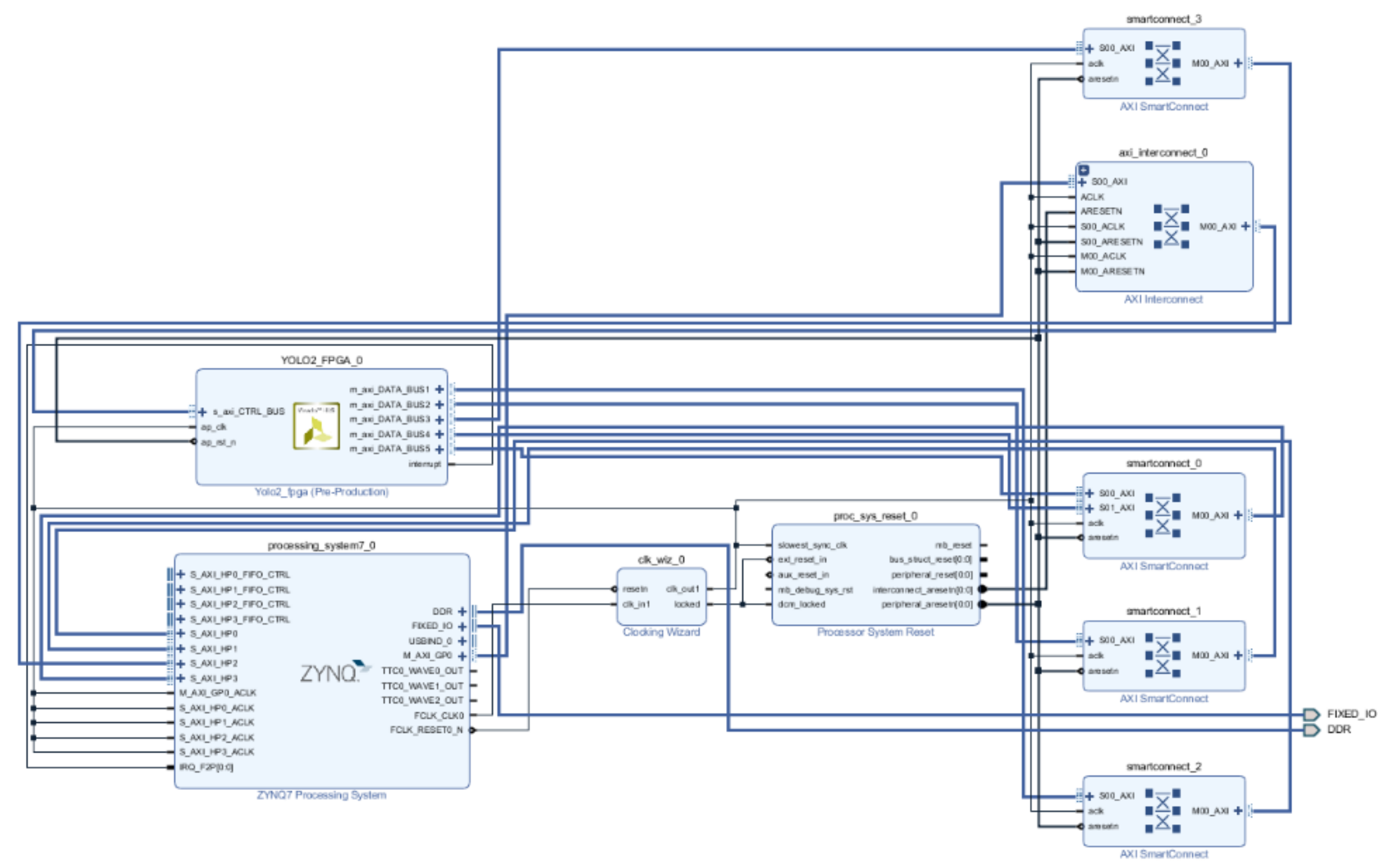
Figure 9 shows a block diagram of the entire FPGA system. The IP synthesized through HLS was connected to the PS for control, and AXI was used to access the DRAM and divided data.
3.2. ASIC Chip
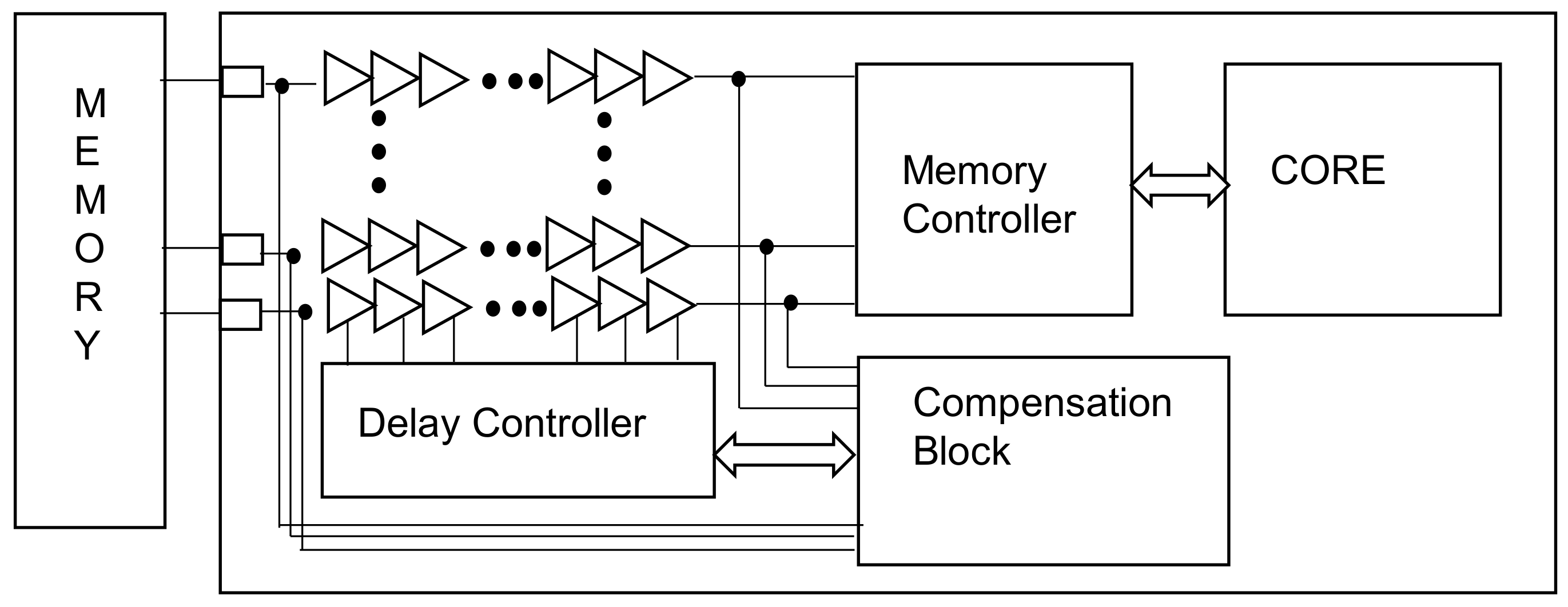
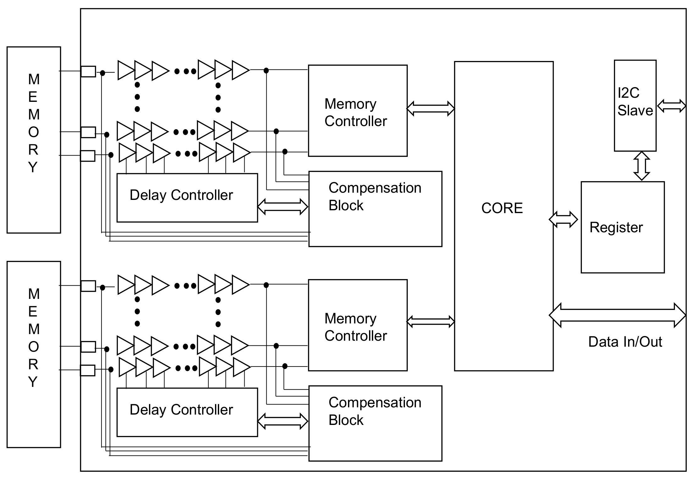
Figure 10 shows the overall chip design. Two memory controllers are connected, and the I2C slave and register are placed inside to control the register chip. The core is a circuit related to image compression.
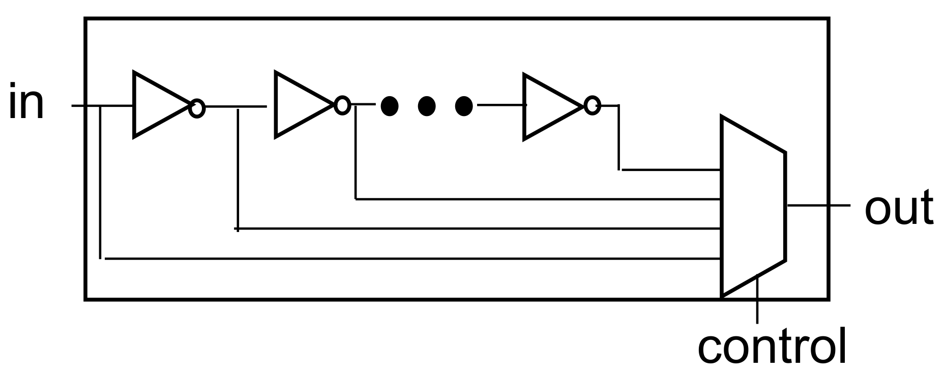
Table 5 shows the composite size of the delay cell and the P&R size of the actual chip. The unit delay cell is the size of the cell used for the two inverters and mux, while the memory controller is the sum of the sizes of some flip-flops and debugging operations inside. The delay control includes logic to add and subtract blocks and other delays that determine the edge.
Table 6 is a comparison between a previous study and this study. The memory system is largely composed of PHY, including IO and a memory controller. In this study, PHY and memory controller were implemented together. The table also shows the results of comparing the gate count of this study, designed with a 65 nm process as one and relatively size. Because processes differ from process company to process company, general Moore’s Law was applied and compared. In [
13], the PHY of LPDDR4 was implemented by the Samsung 10 nm process. Compared to this study, the size was small, but considering the process, the size was approximately three times larger. Moreover, if the implementation of the controller is added, the size is expected to be approximately seven times. [
14] provided a thesis implemented on the controller, excluding PHY, in the memory system. The memory type was not known exactly, but when compared to this paper, a size of approximately four times larger can be determined. [
15] implemented PHY for DDR3. Again, only the PHY was designed, but it was approximately three times larger than that in this study. Although it is difficult to decipher from
Table 6, this study, implemented purely digitally, has two advantages in contrast to [
13,
15]. The first is the time to reach implementation. It is difficult to quantitatively judge the time spent in purely digital design compared to analog circuit design, but considering the layout or simulation time, purely digital design takes much less time to implement. The second is the cost aspect. As mentioned earlier, the cost is reduced because the implementation time is shortened, but there is an effect of reducing the die size because the layout is optimized on the chip.
Table 7 shows the power measurement results. The operation voltage was 1.2 V. “Busy” measured here is the power consumed for reading and writing the data. In particular, a lot of power was consumed in the operation of the IO and the delay cell. In the future, if the delay cell is optimized, less power consumption can be expected.
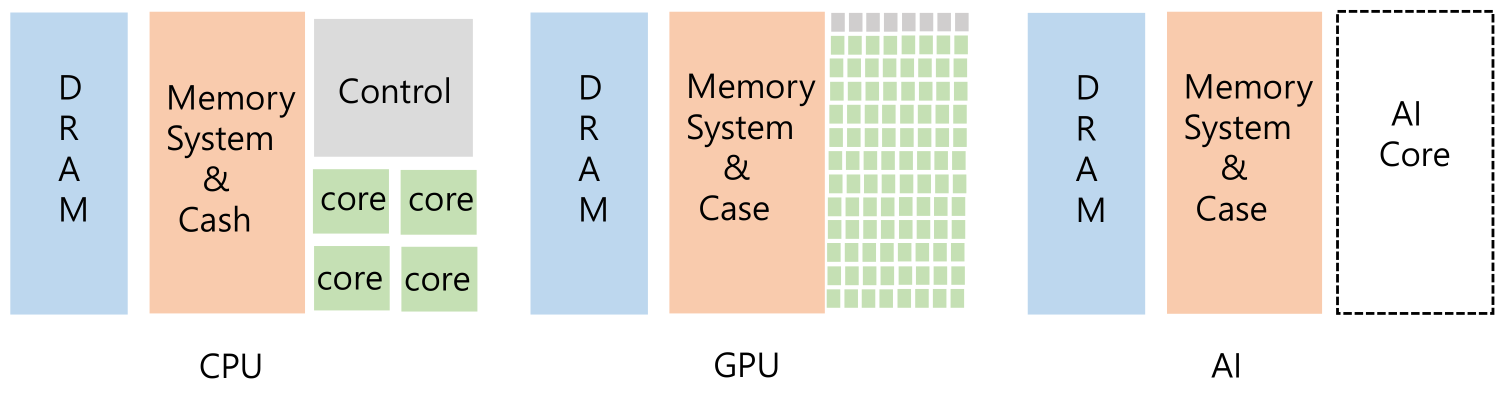
As mentioned in the introduction, the existing AI system does not have its own memory system, but instead uses the memory system used by the GPU or CPU.
Table 8 shows a comparison of the memory used in the existing AI environment and the memory used in this study.
As shown in the results of
Table 3, when YOLO-V2 was implemented in Zedboard, 101 18 kb BRAMs inside the FPGA were used. It is difficult to map the RAM used in the FPGA and the external RAM 1:1, but 18.18 Mb of RAM is used numerically. This means that in a simple AI application such as YOLO-2, a limited memory system is available.
As mentioned in
Section 2, since the first stage of the delay cell is 200 ps, the first stage of the delay cell cannot be accurately measured using an oscilloscope. However, when the delay cell is increased in 10-step units, it is possible to confirm delayed data by the delay cell. In this study, much smaller delay steps could be obtained by using synthesized delay cells rather than analog designs.
Table 9 displays the delay step of our work compared to other studies. The smaller the delay step, the more precisely the skew of the data bus can be adjusted, so the smaller the value that can be adjusted in one step, the better.
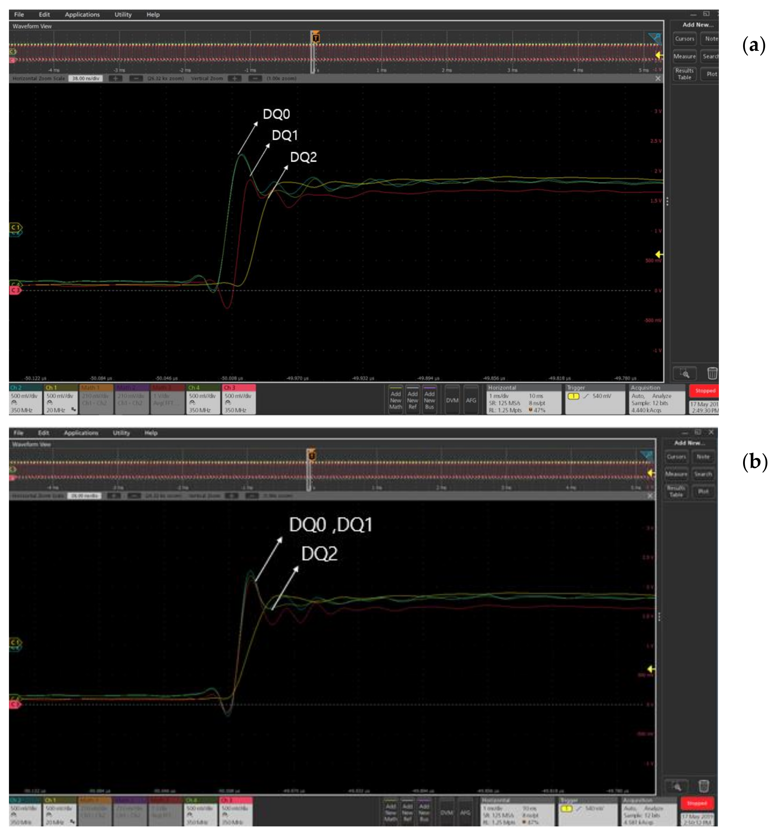
Figure 11 is the result of measuring the data pin using an oscilloscope. A total of three data points were measured at the same time, and a phase difference was deliberately made using a delay controller for the measurement. Looking at
Figure 11a, we can see that the skews of DQ0, DQ1, and DQ2 are different.
Figure 11b shows the result of adjusting the skew by adjusting the delay controller corresponding to DQ1 through I2C.
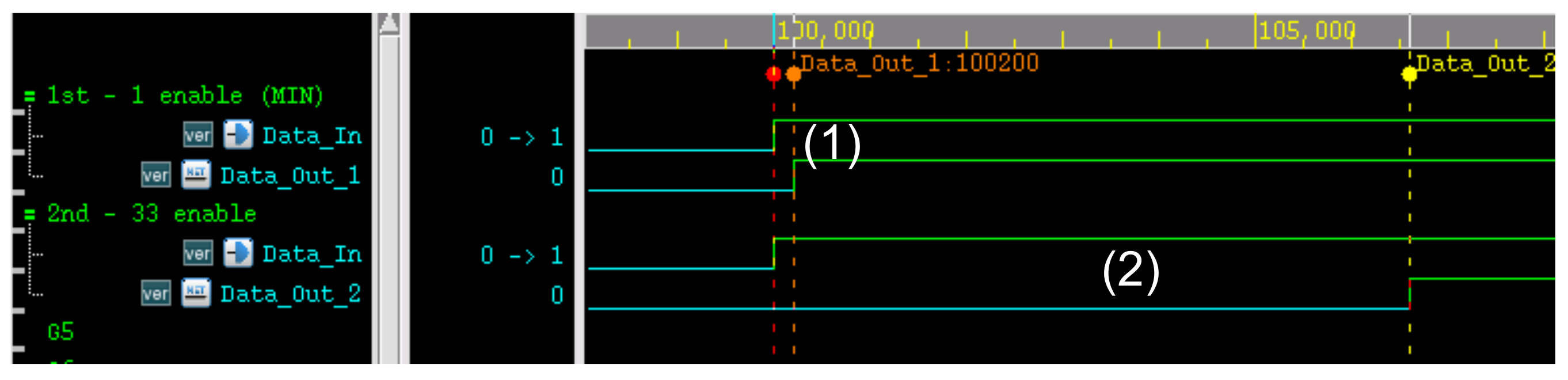
The read and write of the memory can be confirmed indirectly using I2C. If we write the address and data, we want it to register inside the chip through I2C and to write the corresponding pin in the order of
Figure 11, where the data in SDRAM is saved in the register inside the chip. The value was read through the external I2C master and was found to be identical to the value written in the SDRAM.
Table 10 describes the time it takes to read and write data from the external memory. In this study, it was designed to operate from 1 to 100 MHz, but this is the result when measured based on 20 MHz.
The memory used in this study can be used in both 8- and 16-bit modes.
Table 10 describes the time required to read and write 16 and 32 MB.
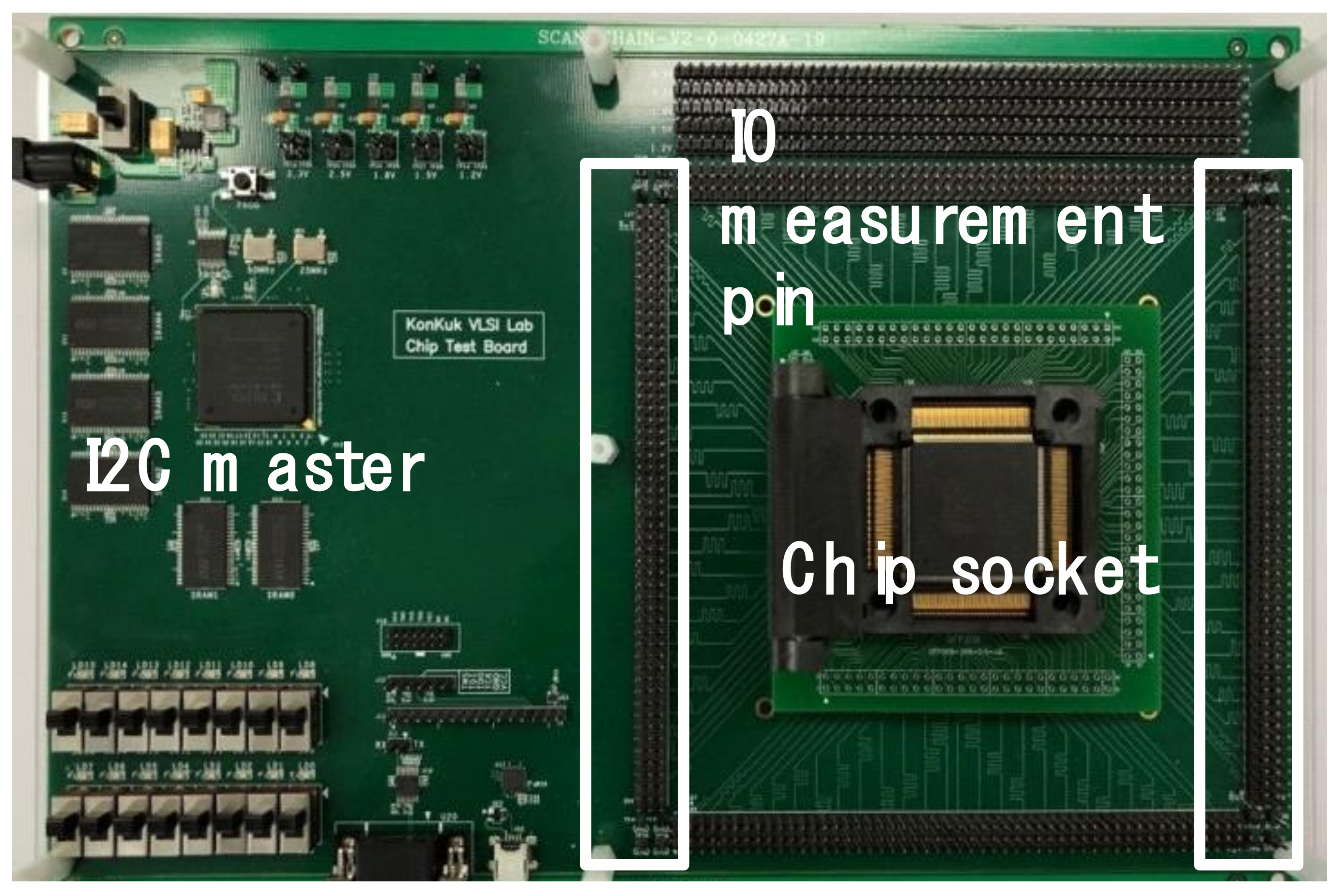
Figure 12 is the environment for measuring the chip. The chip used a socket to enable change, and the FPGA was used to set the environment of the I2C master and measurement board. For measurement, all of the IO of the chip was pulled out with pins.


