Article

Inner Spacer Engineering to Improve Mechanical Stability in Channel-Release Process of Nanosheet FETs

School of Electronics Engineering, Chungbuk National University, Chungdae-ro 1, Cheongju 28644, Korea
*
Author to whom correspondence should be addressed.
Electronics 2021, 10(12), 1395; https://doi.org/10.3390/electronics10121395
Submission received: 6 May 2021 / Revised: 8 June 2021 / Accepted: 9 June 2021 / Published: 10 June 2021
(This article belongs to the Section Microelectronics)

Abstract

:
Mechanical stress is demonstrated in the fabrication process of nanosheet FETs. In particular, unwanted mechanical instability stemming from gravity during channel-release is covered in detail by aid of 3-D simulations. The simulation results show the physical weakness of suspended nanosheets and the impact of nanosheet thickness. Inner spacer engineering based on geometry and elastic property are suggested for better mechanical stability. The formation of wide contact area between inner spacer and nanosheet, as well as applying rigid spacer dielectric material, are preferred.

1. Introduction

As logic technology continues scaling for smaller chip size, better output performance, and low static power consumption, channel geometry in field-effect transistors (FETs) have evolved from planar to nanowire structures, as is well known. Gate-all-around (GAA) field-effect transistors (FETs) show better gate controllability and short-channel effects (SCEs) suppression than FinFETs do [1]. However, due to the limitation of nanowire perimeter in GAA FETs, vertically stacked structures comprising multiple silicon nanowires or nanosheets have been preferred for wider effective channel width [2,3,4]. Compared with FinFETs, stacked GAAs require formation of channels suspended from substrate. Generally, fabrication methods for suspended channels have been categorized in two ways. The first approach is to use a sacrificial layer deposited on a substrate such as a dielectric (e.g., SiO2) or inorganic layer (e.g., SixGe1−x) [5,6,7]. Silicon channels can be suspended from the substrate when the sacrificial layer is selectively wet-etched. The second approach is to use reactive dry etching, called the ‘Bosch process’, to form stacked channels [2,8]. Sequentially performed isotropic dry etching, thermal oxidation, and removal of sacrificial oxide are used to form suspended channels.
However, both the above-mentioned approaches to form suspended channels encountered a mechanical instability, known as stiction, which is associated with the capillary force of chemicals during wet-etching [9]. Fortunately, this concern has been avoided by improved dry etching and supercritical drying [10,11,12,13]. The other concern during the suspension of channels is vertical stress associated with gravity. Nanosheet FETs (NS FETs), due to their wider perimeter and larger volume, have much heavier channel mass than that of nanowire FETs. Even though stiction can be avoided by aid of the several knobs mentioned above, improvements against gravity have been modest so far. Most research about NS FETs has focused on improvements of electrical performances in terms of DC or AC [14,15]. In this context, discussions on mechanical stability and implementing improvements seem timely in the development of NS FETs.
In this work, for the first time, the impact of gravity during fabrication processing of NS FETs is demonstrated. In particular, we discuss the mechanical displacement of nanosheets when channels are released. The results are quantitively analyzed by aid of a 3-D numerical simulator. Based on the results, fabrication guidelines in terms of inner spacer engineering are suggested to improve mechanical stability of NS FETs.

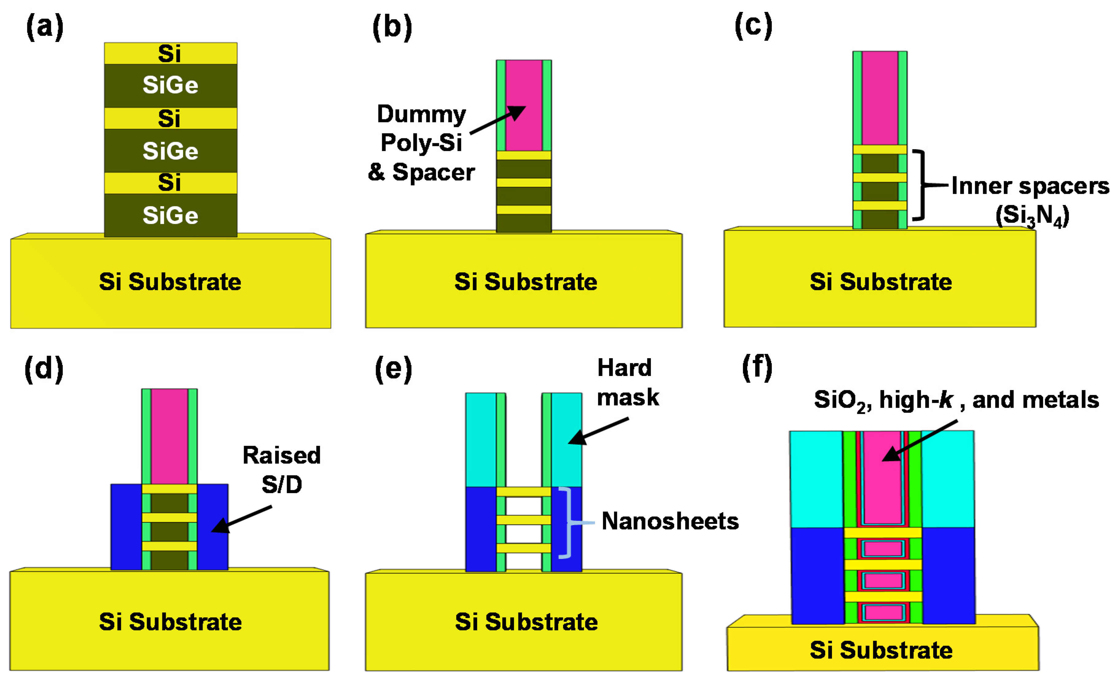
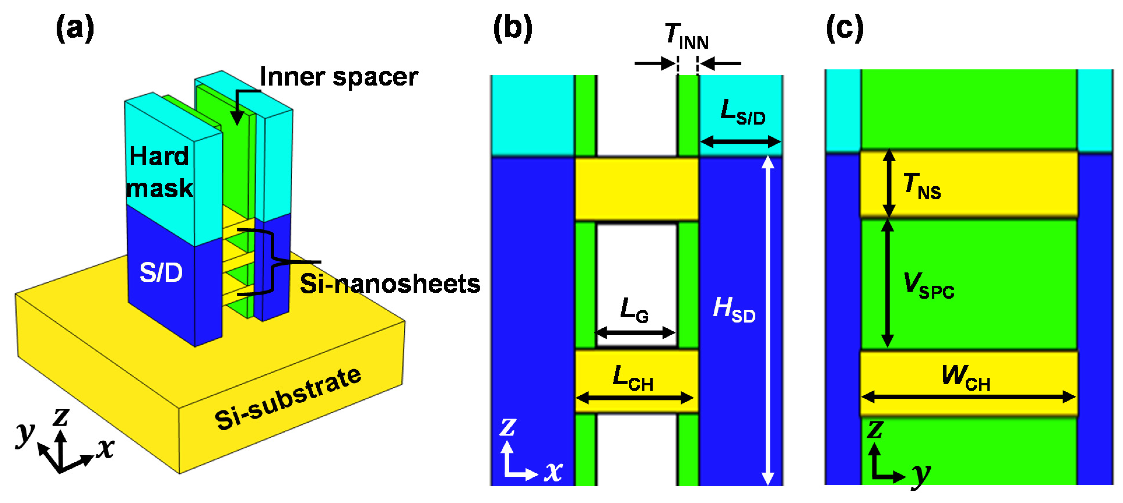
2. Materials and Methods
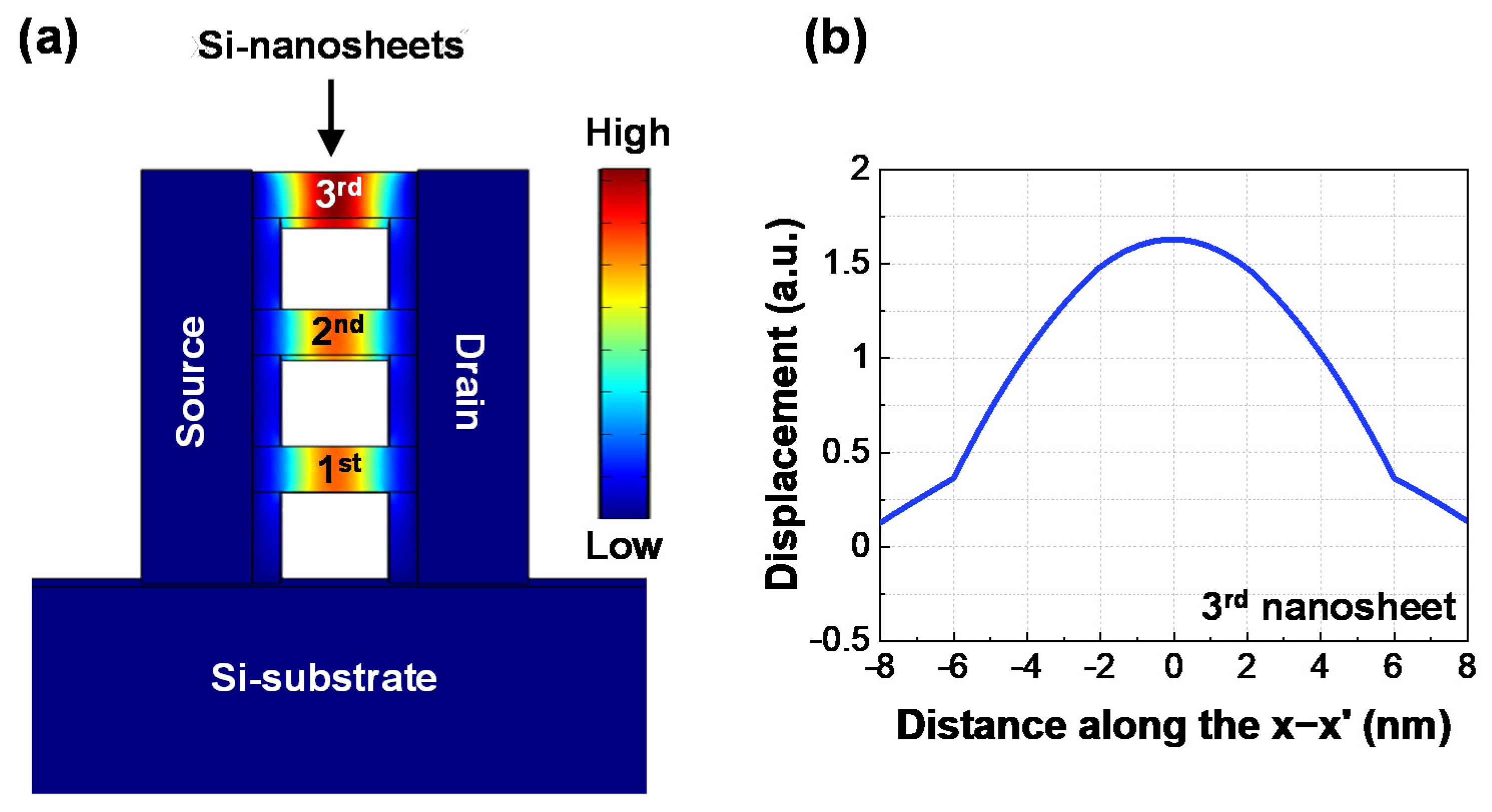
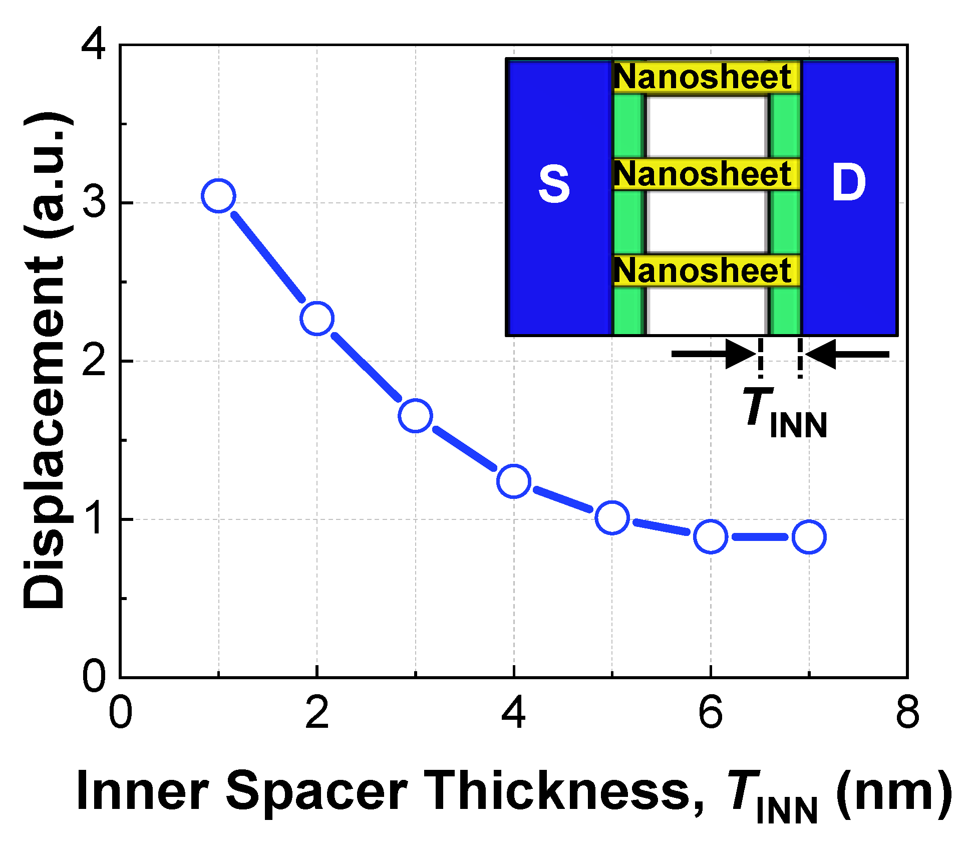
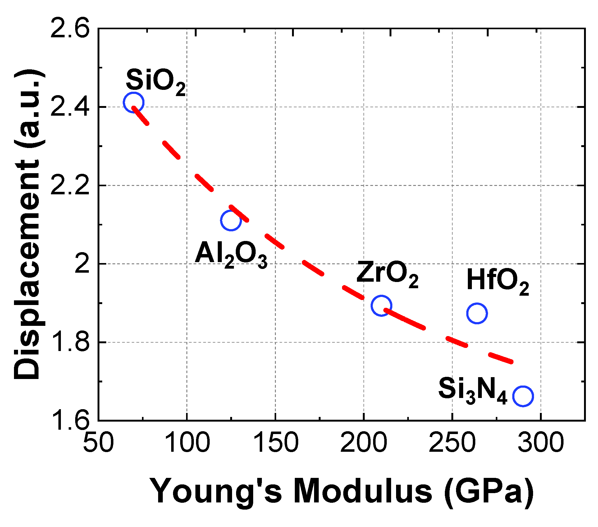
Figure 1 provides a summary of the fabrication process of NS FETs. Si/SixGe1−x stacks are iteratively deposited on a substrate by epitaxial growth. Then, a dummy gate composed of poly-Si is deposited as a hard mask. Thereafter, Si/SixGe1−x stacks are dry etched for source/drain (S/D) formation. SixGe1−x indent etching, inner spacer deposition, and heavily doped silicon formation at the S/D are sequentially performed. There is no critical concern until the step shown in Figure 1d, but mechanical failure occurs among the nanosheets during channel-release, as shown in Figure 1e. In this context, our simulation studies were performed under the situation shown in Figure 1e. Summary of device fabrication processing with 3-dimensional graphics has been reported in previous works, in detail [16,17].
Figure 2 provides a schematic diagram of an NS FET for mechanical simulation. The device has three suspended nanosheet channels; the gate length (LG), channel width (WCH), and channel-to-channel vertical space (VSPC) are 12 nm, 30 nm, and 10 nm, respectively. The three-dimensional (3-D) numerical simulator COMSOL was utilized with the solid mechanics module. The mesh size was defined as 2 nm. Dominant material parameters to determine the simulation result were Young’s modulus, Poisson ratio, and density. All simulations were performed under a steady-state condition. Moreover, the substrate, raised S/D, and its hard mask were supposed to be free from mechanical stress to observe the mechanical behavior in nanosheets. Gravity, which is the most important parameter in this simulation, was applied in all structures. Detailed device geometry and material properties are summarized in Table 1.

3. Results

Figure 3 shows the simulation results of mechanical stress when the nanosheets were released. As there is no filling material underneath the nanosheets, mechanical displacement was concentrated in the middle of each nanosheet. In addition, in terms of location of the spot, there was no difference between the nanosheet at the first floor and that of the third floor. Considering that the process to form suspended multiple nanosheets (or nanowires) is very difficult to control due to adhesion between nanosheets [14], this result would be informative during device fabrication. Figure 4 shows the simulation results for various nanosheet thicknesses (TNS). Considering stacked nanosheets, more than five stories are preferred for better performance of logic, and channel thickness should be thinner under the same S/D height (HSD) [18]. However, the mechanical displacement abruptly increased as TNS was reduced to less than 3 nm. According to the material mechanics, the section moment of inertia (I) is an important factor for flexural rigidity. The flexural rigidity (D) and I can be described by,
I = 1 12 W CH T CH 3
D = E I
where E is Young’s modulus [19]. It was found that mechanical deformation could be reduced when TNS is thick, because of increased D. In the case of an n-type NS FET, a few nanometers of inner spacer is deposited between the nanosheets. Currently, most reports related with inner spacer have been performed in terms of electrical performance [20,21,22,23,24]. However, in view of the mechanical stress, the inner spacer plays a large role in the support of each nanosheet.
As inner spacer thickness (TINN) changes from 3 nm to 1 nm, the mechanical deformation increased 1.8 times due to increased vacuum area underneath each nanosheets (Figure 5). It should be noted that typical shape of inner spacer is not rectangular but close to that of a ribbon because of the process limitations [14].
Figure 6 shows that the magnitude of mechanical displacement depends on the contact area between the inner spacer and the nanosheet. Compared with the rectangular shape (contact area = 3 nm), the semicircle shape inner spacer (contact area = 0 nm) shows two times higher stress due to lack of vertical support. Hence, the rectangular shape of inner spacer is preferred despite the difficult fabrication process. Alternatively, inner space engineering can be performed via material engineering, as shown in Figure 7. As the Young’s modulus of the inner spacer increases, mechanical strength of the dielectric layer becomes rigid and strong; hence, the stability of suspended nanosheets can be improved.

4. Conclusions

Mechanical stability stemming from gravity was demonstrated in the fabrication process of nanosheet FETs (NS FETs) during channel-release. Mechanical displacement was concentrated in the middle of each nanosheet, and depended on the nanosheet thickness (TNS), inner spacer geometry, and materials. As a result, increasing the inner spacer thickness and contact area at the inner spacer/nanosheet interface is preferred. Moreover, applying an inner spacer with high Young’s modulus can be a possible alternative for better mechanical stability.

Author Contributions

J.-Y.P. conceived this project and designed all the experiments. K.-S.L. conducted all the simulations including mechanical displacement, and wrote this paper. Both authors have read and agreed to the published version of the manuscript.

Funding

This work was supported by the National Research Foundation (NRF) of Korea grant funded by the Korea government (MSIT) (No. 2020M3H2A1076786 and 2021R1F1A1049456). The EDA tool was supported by the IC Design Education Center (IDEC), Republic of Korea. K.-S. Lee and J.-Y Park are with the School of Electronics Engineering, Chungbuk National University, Chungdae-ro 1, Cheongju, Chungbuk 28644, Republic of Korea.

Conflicts of Interest

The authors declare no conflict of interest.

References

  1. Zhang, S. Review of Modern Field Effect Transistor Technologies for Scaling. J. Phys. Conf. Ser. 2020, 1617, 012054. [Google Scholar] [CrossRef]
  2. Ng, R.M.Y.; Wang, T.; Liu, F.; Zuo, X.; He, J.; Chan, M. Vertically Stacked Silicon Nanowire Transistors Fabricated by Inductive Plasma Etching and Stress-Limited Oxidation. IEEE Electron Device Lett. 2009, 30, 520–522. [Google Scholar] [CrossRef]
  3. Lee, S.-Y.; Kim, S.-M.; Yoon, E.-J.; Oh, C.-W.; Chung, I.; Park, D.; Kim, K. A novel multibridge-channel MOSFET (MBCFET): Fabrication technologies and characteristics. IEEE Trans. Nanotechnol. 2003, 2, 253–257. [Google Scholar] [CrossRef]
  4. Thomas, S. Nanosheet FETs at 3 nm. Nat. Electron. 2018, 1, 613–614. [Google Scholar] [CrossRef]
  5. Colinge, J.; Gao, M.; Romano-Rodriguez, A.; Maes, H.; Claeys, C. Silicon-on-insulator “gate-all-around device”. In Proceedings of the 1990 International Electron Devices Meeting (IEDM), San Francisco, CA, USA, 9–12 December 1990; pp. 595–598. [Google Scholar]
  6. Bera, L.K.; Nguyen, H.S.; Singh, N.; Liow, T.Y.; Huang, D.X.; Hoe, K.M.; Tung, C.H.; Fang, W.W.; Rustagi, S.C.; Jiang, Y.; et al. Three Dimensionally Stacked SiGe Nanowire Array and Gate-All-Around p-MOSFETs. In Proceedings of the 2006 International Electron Devices Meeting (IEDM), San Francisco, CA, USA, 9–13 December 2006; pp. 551–554. [Google Scholar]
  7. Lee, S.-Y.; Kim, S.-M.; Yoon, E.-J.; Oh, C.W.; Chung, I.; Park, D.; Kim, K. Three-Dimensional MBCFET as an Ultimate Transistor. IEEE Electron Device Lett. 2004, 25, 217–219. [Google Scholar] [CrossRef]
  8. Sacchetio, D.; Ben-Jamaal, M.H.; de Michelil, G.; Leblebici, Y. Fabrication and Characterization of Vertically Stacked Gate-All-Around Si Nanowire FET Arrays. In Proceedings of the 2009 Proceedings of the European Solid State Device Research Conference, Athens, Greece, 14–18 September 2009; pp. 245–248. [Google Scholar]
  9. Bustillo, J.; Howe, R.; Muller, R. Surface micromachining for microelectromechanical systems. Proc. IEEE 1998, 86, 1552–1574. [Google Scholar] [CrossRef] [Green Version]
  10. Mertens, H.; Ritzenthaler, R.; Pena, V.; Santoro, G.; Kenis, K.; Schulze, A.; Litta, E.D.; Chew, S.A.; Devriendt, K.; Demuynck, S.; et al. Vertically Stacked Gate-All-Around Si Nanowire Transistors: Key Process Optimizations and Ring Oscillator Demonstration. In Proceedings of the 2017 IEEE International Electron Devices Meeting (IEDM), San Francisco, CA, USA, 2–6 December 2017; pp. 828–831. [Google Scholar]
  11. Loubet, N.; Kal, S.; Alix, C.; Pancharatnam, S.; Zhou, H.; Durfee, C.; Belyansky, M.; Haller, N.; Watanabe, K.; Devarajan, T.; et al. A Novel Dry Selective Etch of SiGe for the Enablement of High Performance Logic Stacked Gate-All-Around NanoSheet Devices. In Proceedings of the 2019 IEEE International Electron Devices Meeting (IEDM), San Francisco, CA, USA, 7–11 December 2019. [Google Scholar]
  12. Lee, B.-H.; Kang, M.-H.; Ahn, D.-C.; Park, J.-Y.; Bang, T.; Jeon, S.-B.; Hur, J.; Lee, D.; Choi, Y.-K. Vertically integrated multiple nanowire field effect transistor. Nano Lett. 2015, 15, 8056–8061. [Google Scholar] [CrossRef] [PubMed]
  13. Hwang, K.-M.; Park, J.-Y.; Bae, H.; Lee, S.-W.; Kim, C.-K.; Seo, M.; Im, H.; Kim, D.-H.; Kim, S.-Y.; Lee, G.-B.; et al. Nano-electromechanical Switch Based on a Physical Unclonable Function for Highly Robust and Stable Performance in Harsh Environments. ACS Nano 2016, 11, 12547–12552. [Google Scholar] [CrossRef] [PubMed]
  14. Loubet, N.; Hook, T.; Montanini, P.; Yeung, C.-W.; Kanakasabapathy, S.; Guillom, M.; Yamashita, T.; Zhang, J.; Miao, X.; Wang, J.; et al. Stacked nanosheet gate-all-around transistor to enable scaling beyond FinFET. In Proceedings of the 2017 Symposium on VLSI Technology, Kyoto, Japan, 5–8 June 2017; pp. T230–T231. [Google Scholar]
  15. Bae, G.; Bae, D.-I.; Kang, M.; Hwang, S.M.; Kim, S.S.; Seo, B.; Kwon, T.Y.; Lee, T.J.; Moon, C.; Choi, Y.M.; et al. 3 nm GAA Technology Featuring Multi-Bridge-Channel FET for Low Power and High Performance Applications. In Proceedings of the 2018 IEEE International Electron Devices Meeting (IEDM), San Francisco, CA, USA, 1–5 December 2018; pp. 28.7.1–28.7.4. [Google Scholar]
  16. Li, J.; Li, Y.; Zhou, N.; Xiong, W.; Wang, G.; Zhang, Q.; Du, A.; Gao, J.; Kong, Z.; Lin, H.; et al. Study of Silicon Nitride Inner Spacer Formation in Process of Gate-all-around Nano-Transistors. Nanomaterials 2020, 10, 703. [Google Scholar] [CrossRef] [PubMed]
  17. Kal, S.; Pereira, C.; Oniki, Y.; Holsteyns, F.; Smith, J.; Mosden, A.; Kumar, K.; Biolsi, P.; Hurd, T. Selective isotropic etching of Group IV semiconductors to enable gate all around device architectures. In Proceedings of the Surface Preparation and Cleaning Conference (SPCC), Cambridge, MA, USA, 10–11 April 2018. [Google Scholar]
  18. Barraud, S.; Previtali, B.; Vizioz, C.; Hartmann, J.M.; Sturm, J.; Lassarre, J.; Perrot, C.; Rodriguez, P.; Loup, V.; Magalhaes-Lucas, A.; et al. 7-Levels-Stacked Nanosheet GAA Transistors for High Performance Computing. In Proceedings of the 2020 IEEE Symposium on VLSI Technology, Honolulu, HI, USA, 16–19 June 2020; pp. 1–2. [Google Scholar]
  19. Zheng, X.; Wang, Q.; Zhang, R.; Ma, L.; Luan, J. Effects of aspect ratio and metal layer thickness on demoulding of metal/polymer bi-layer gratings during nanoimprinting. Sci. Rep. 2018, 8, 12720. [Google Scholar] [CrossRef] [PubMed]
  20. Ryu, D.; Myeong, I.; Lee, J.K.; Kang, M.; Jeon, J.; Shin, H. Investigation of Gate Sidewall Spacer Optimization From OFF-State Leakage Current Perspective in 3-nm Node Device. IEEE Trans. Electron Devices 2019, 66, 2532–2537. [Google Scholar] [CrossRef]
  21. Kim, S.; Kim, M.; Ryu, D.; Lee, K.; Kim, S.; Lee, J.; Lee, R.; Kim, S.; Lee, J.H.; Park, B.G. Investigation of Electrical Characteristic Behavior Induced by Channel-Release Process in Stacked Nanosheet Gate-All-Around MOSFETs. IEEE Trans. Electron Devices 2020, 67, 2648–2652. [Google Scholar] [CrossRef]
  22. Ryu, D.; Kim, M.; Kim, S.; Choi, Y.; Donghyun, R.; Lee, J.-H.; Park, B.-G. Design and Optimization of Triple-k Spacer Structure in Two-Stack Nanosheet FET from OFF-State Leakage Perspective. IEEE Trans. Electron Devices 2020, 67, 1317–1322. [Google Scholar] [CrossRef]
  23. Shen, T.; Watanabe, K.; Zhou, H.; Belyansky, M.; Struckert, E.; Zhang, J.; Greene, A.; Basker, V.; Wang, M. A new tech-nique for evaluating stacked nanosheet inner spacer TDDB reliability. In Proceedings of the 2020 IEEE International Reliability Physics Symposium (IRPS), Dallas, TX, USA, 28 April–30 May 2020; pp. 1–5. [Google Scholar]
  24. Yoon, J.-S.; Baek, R.-H. Device Design Guideline of 5-nm-Node FinFETs and Nanosheet FETs for Analog/RF Applications. IEEE Access 2020, 8, 189395–189403. [Google Scholar] [CrossRef]
Figure 1. Summary of fabrication process flow of nanosheet FETs (NMOS). (a) Si/SixGe1−x stacking by iterative epitaxial growth. (b) Dummy poly-Si gate patterning and source/drain dry etching. (c) Si/SixGe1−x in-dent etching and inner spacer deposition. (d) Epitaxial growth for source and drain. (e) Replacement of poly-Si gate and channel-release by selective dry etching. (f) Gate stack formation including high-k, dipole engineering, and work function metals.
Electronics 10 01395 g001
Figure 2. (a) Schematic geometry of Figure 1e for mechanical simulations. (b) Cross-sectional view of structure along x-direction. (c) Cross-sectional view of structure along the y-direction.
Electronics 10 01395 g002
Figure 3. (a) Simulated mechanical displacement profiles from Figure 1e and Figure 2. (b) Extracted mechanical displacement along the x–x’ direction.
Electronics 10 01395 g003
Figure 4. Extracted mechanical displacement with various channel thicknesses.
Electronics 10 01395 g004
Figure 5. Extracted mechanical displacement with inner spacer thickness (TINN).
Electronics 10 01395 g005
Figure 6. Extracted mechanical displacement with inner space geometry. TINN was fixed at 3 nm.
Electronics 10 01395 g006
Figure 7. Mechanical displacement with various possible inner spacer materials.
Electronics 10 01395 g007
Table 1. Parameters for Mechanical Simulation.
ParameterValueMaterial
Gate Length, LG12 nmVacuum
Channel Width, WCH30 nmSi
Channel-to-Channel Vertical Space, VSPC10 nmVacuum
Nanosheet Thickness, TNS5 nmSi
Inner Spacer Thickness, TINN3 nmSi3N4
Source/Drain Length, LSD12 nmSi
Source/Drain Height, HSD 45 nmSi
Substrate100 nm× 100 nm× 30 nmSi
Publisher’s Note: MDPI stays neutral with regard to jurisdictional claims in published maps and institutional affiliations.

