Author Contributions
Conceptualization, supervision, and funding acquisition, J.O.; methodology, N.T.B.; software, N.T.B., G.Y.A., T.T.N.D., and Q.C.B.; validation, and J.O.; writing—original draft preparation, N.T.B., T.M.T.N., S.P., D.T.P., J.C., and T.T.H.V., writing—review and editing, all authors. All authors have read and agreed to the published version of the manuscript.
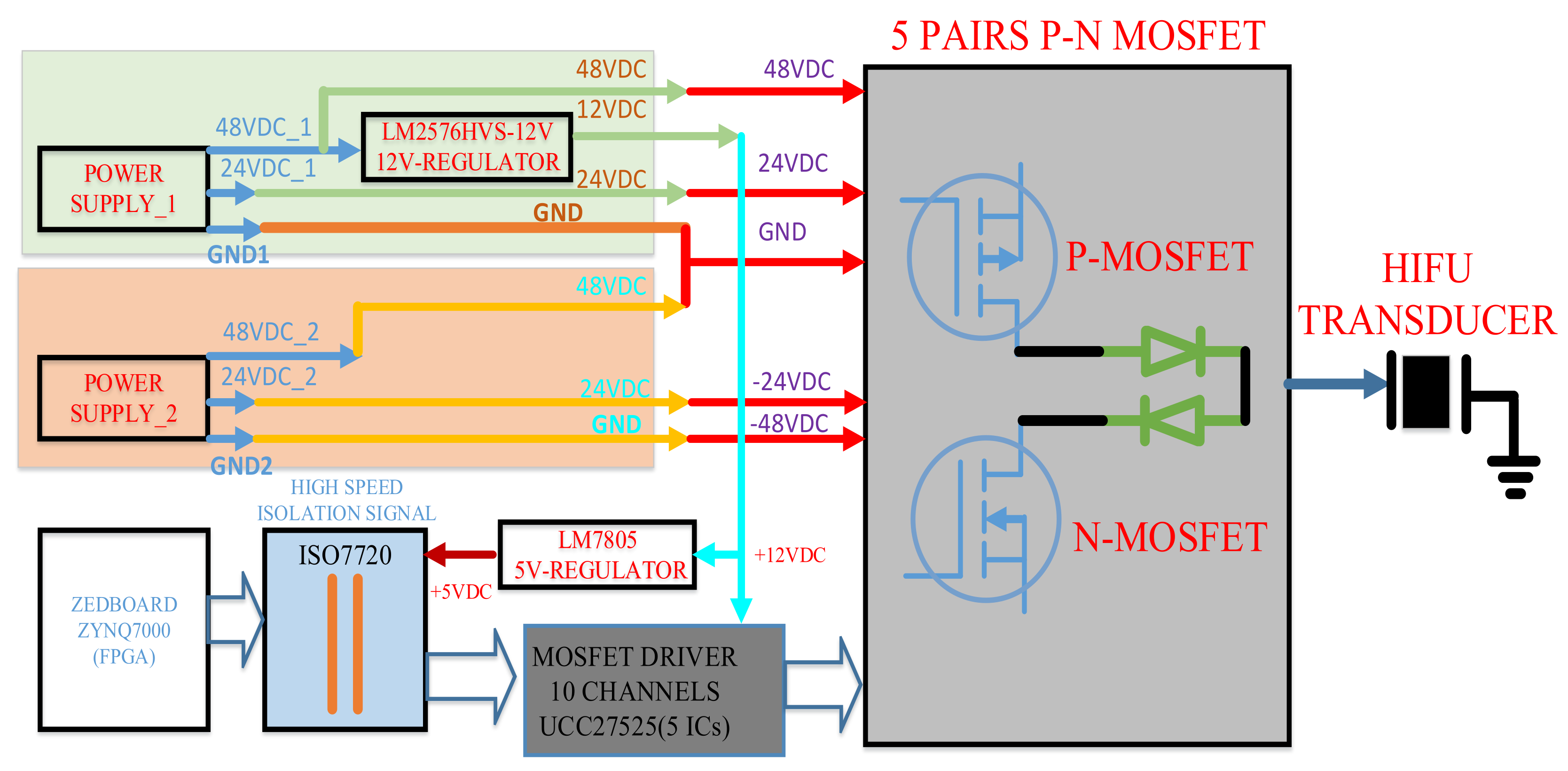
Figure 1.
Proposed HIFU controller system.
Figure 1.
Proposed HIFU controller system.
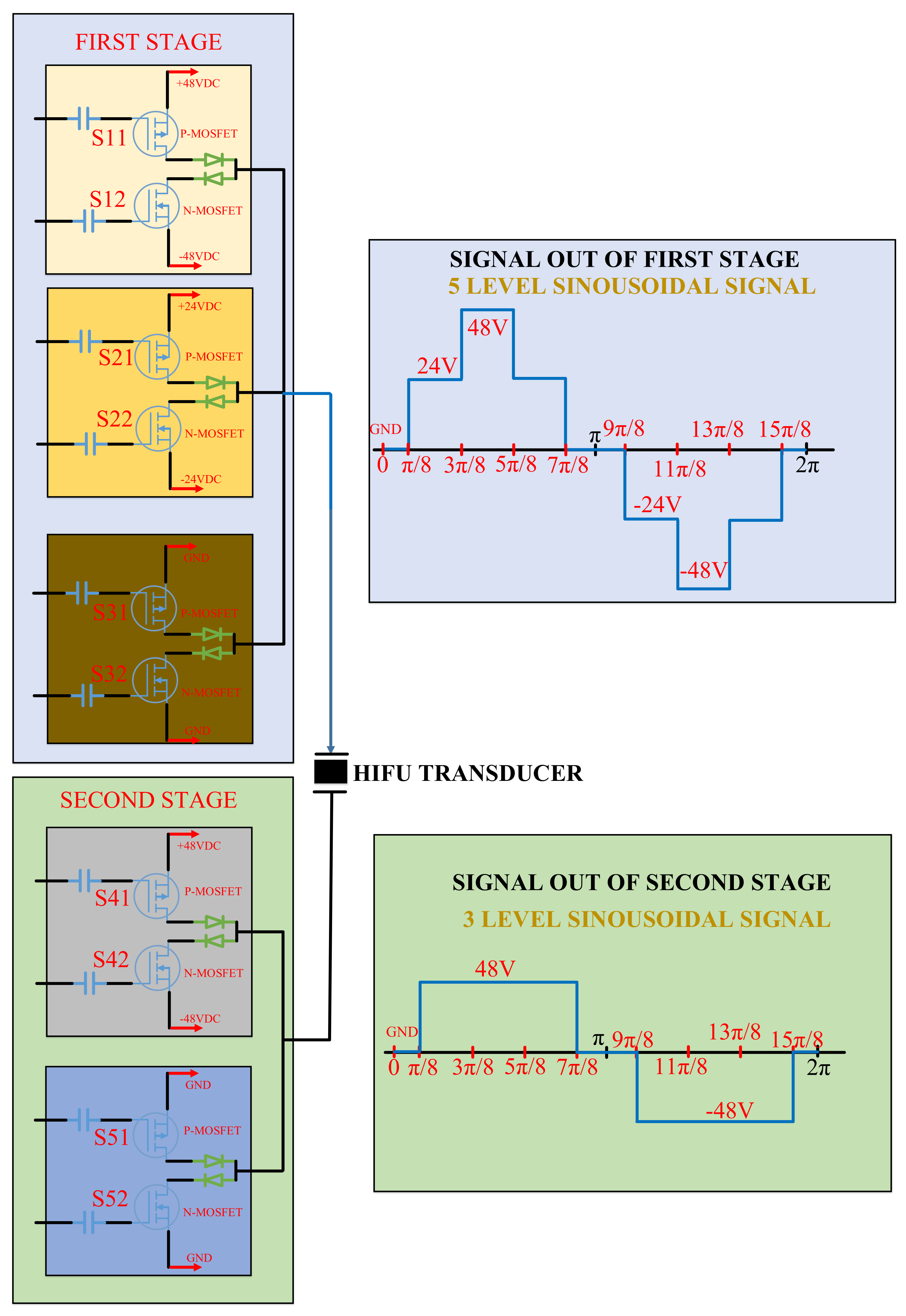
Figure 2.
Proposed HIFU signal generator method.
Figure 2.
Proposed HIFU signal generator method.
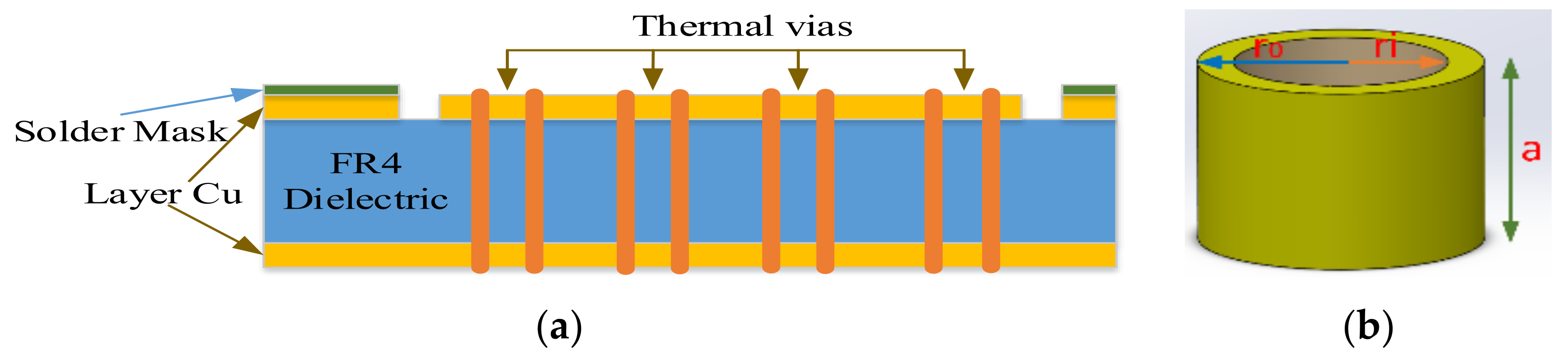
Figure 3.
(a) Structure of two-layered FR-4 PCB with thermal vias; (b) thermal vias.
Figure 3.
(a) Structure of two-layered FR-4 PCB with thermal vias; (b) thermal vias.
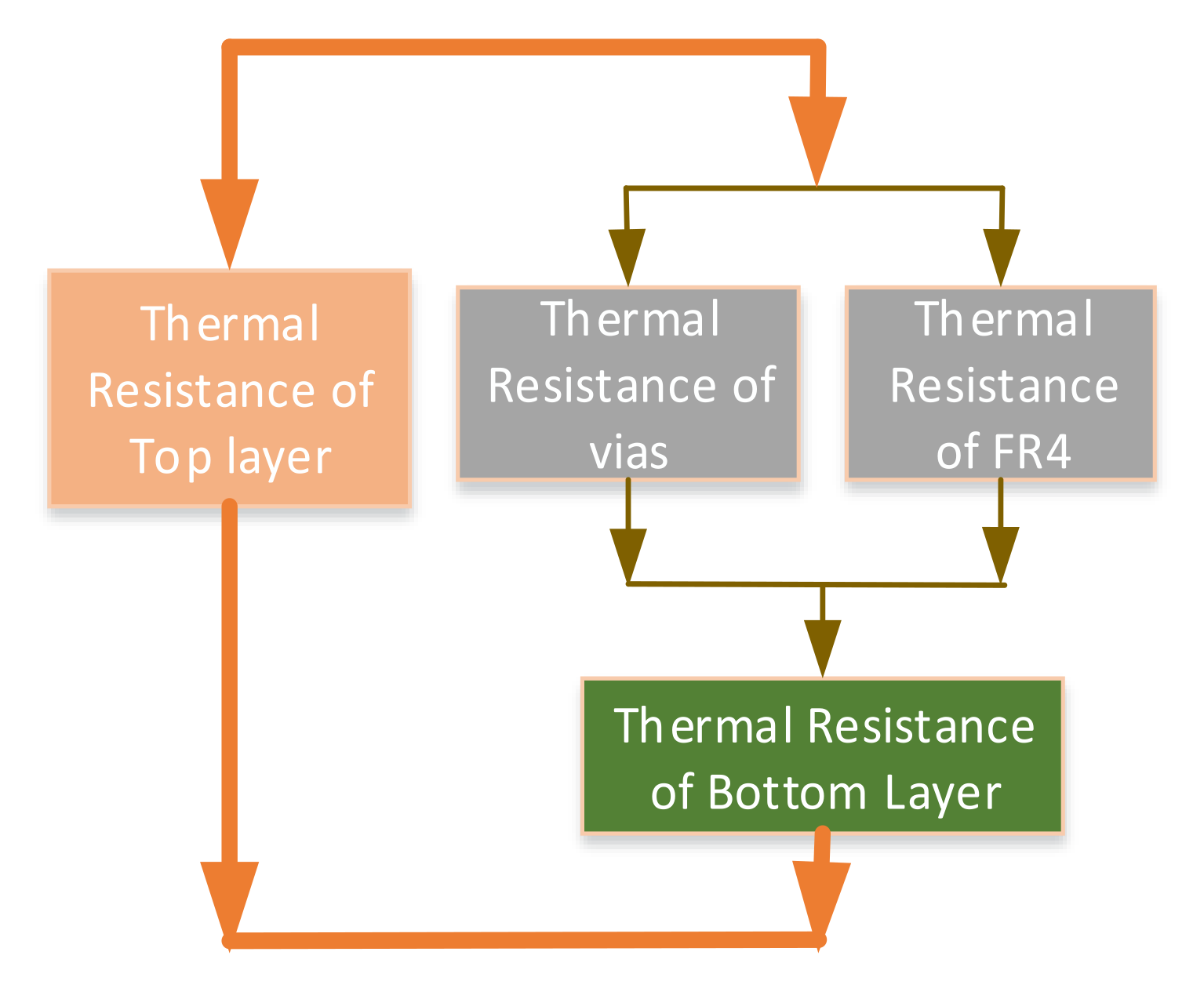
Figure 4.
Schematic thermal resistance of the two PCB layers.
Figure 4.
Schematic thermal resistance of the two PCB layers.
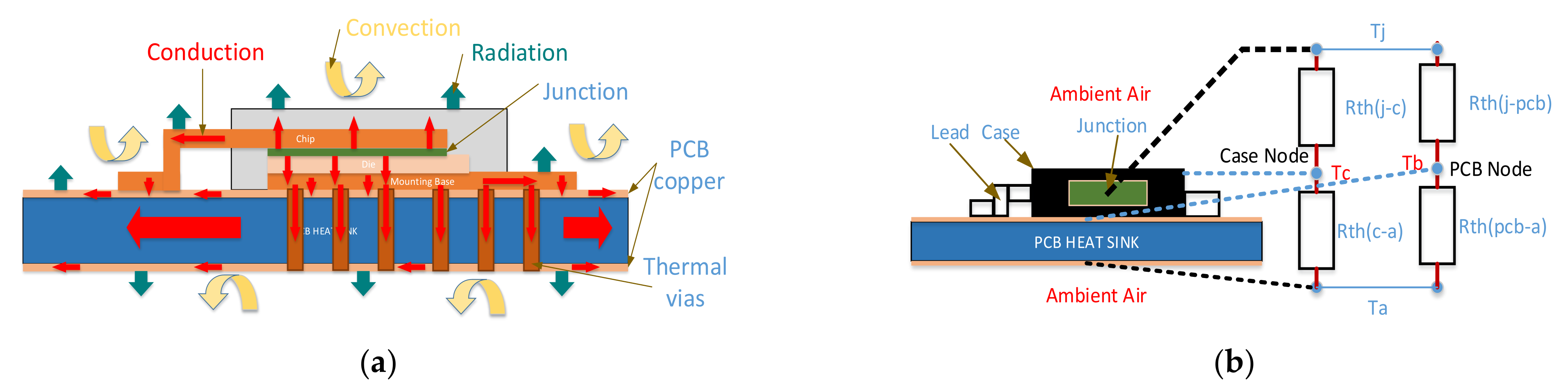
Figure 5.
(a) Heat dissipate inside IC to copper of PCB and surface of PCB to the air; (b) schematic thermal resistance of two PCB layers and the SMD component.
Figure 5.
(a) Heat dissipate inside IC to copper of PCB and surface of PCB to the air; (b) schematic thermal resistance of two PCB layers and the SMD component.
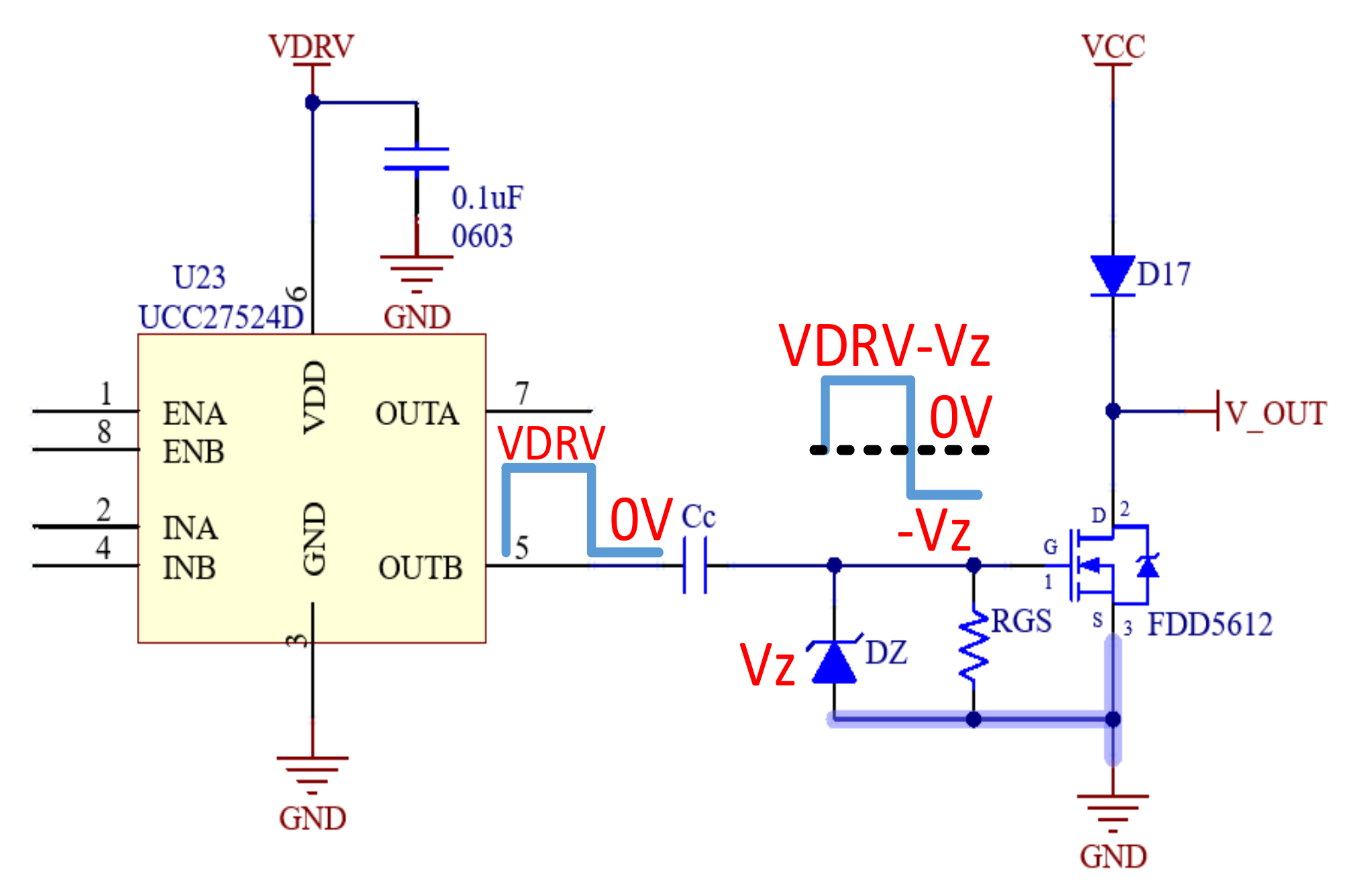
Figure 6.
Proposed MOSFET driver circuit for the HIFU system [
37].
Figure 6.
Proposed MOSFET driver circuit for the HIFU system [
37].
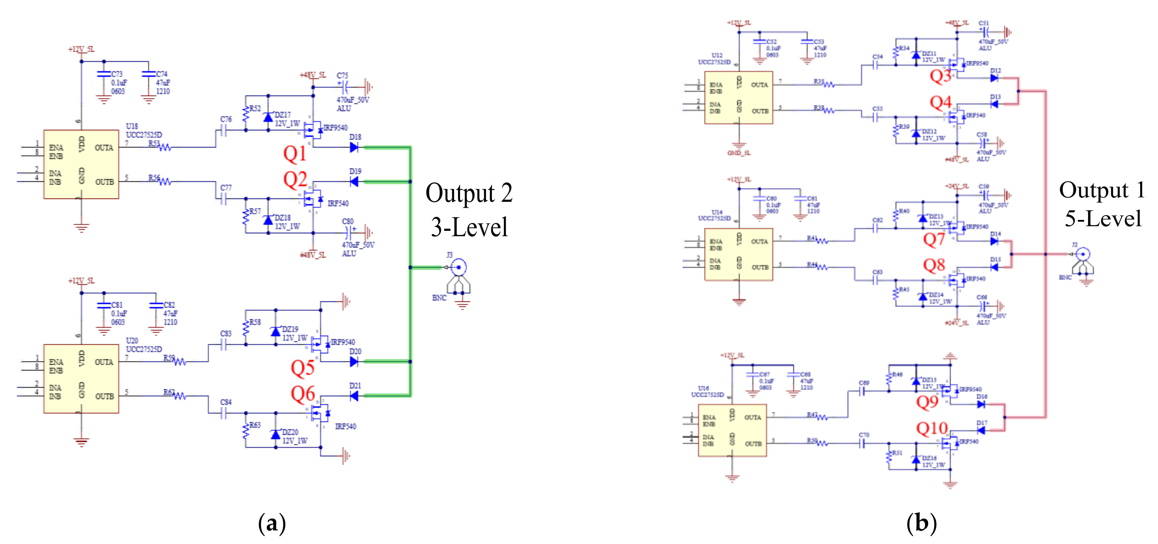
Figure 7.
Proposed HIFU high-power signal generator circuit: (a) output with 3 level, (b) output with 5 level.
Figure 7.
Proposed HIFU high-power signal generator circuit: (a) output with 3 level, (b) output with 5 level.
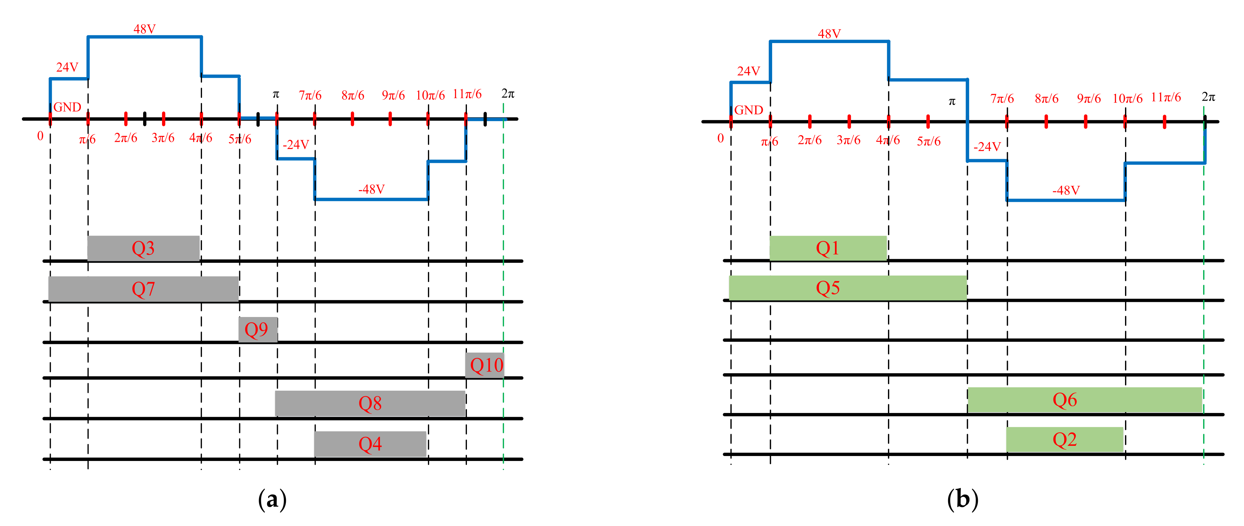
Figure 8.
Proposed sinusoidal signal generator method: (a) five-level, (b) four-level.
Figure 8.
Proposed sinusoidal signal generator method: (a) five-level, (b) four-level.
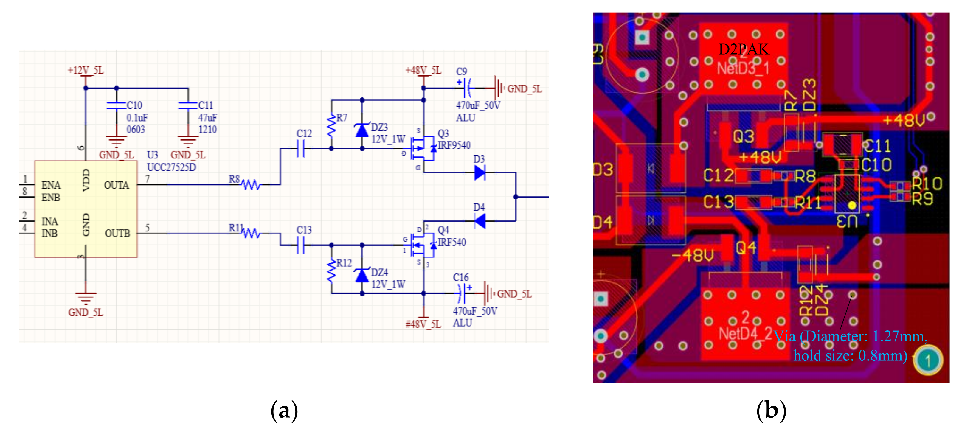
Figure 9.
Proposed MOSFET pair driver circuit for the HIFU system: (a) schematic; and (b) layout with copper thermal dissipation area and thermal vias.
Figure 9.
Proposed MOSFET pair driver circuit for the HIFU system: (a) schematic; and (b) layout with copper thermal dissipation area and thermal vias.
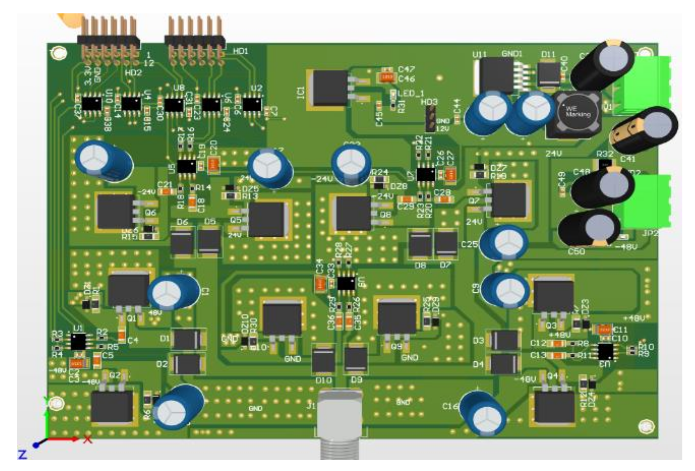
Figure 10.
3D layout of the HIFU high-power signal generator circuit.
Figure 10.
3D layout of the HIFU high-power signal generator circuit.
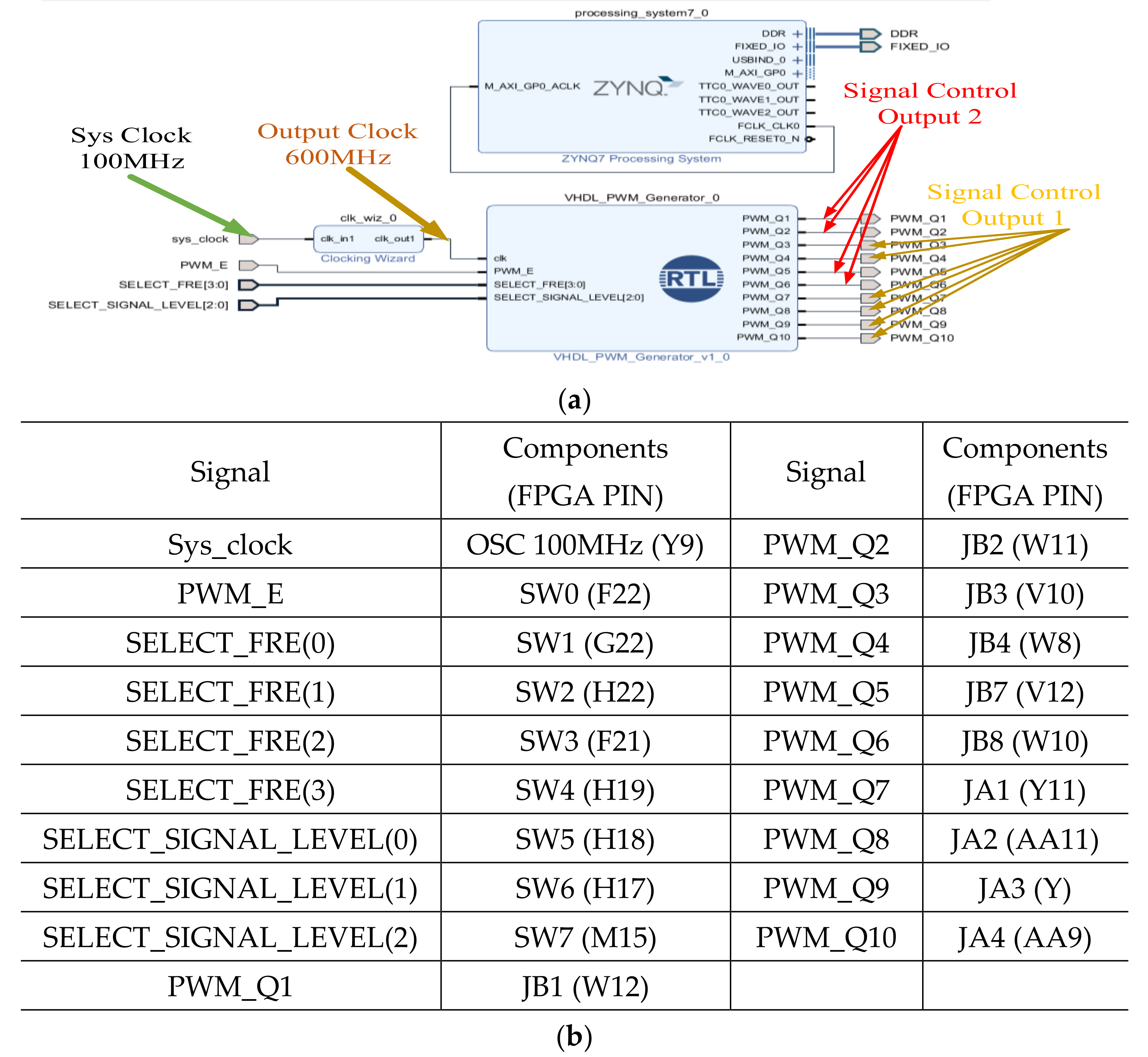
Figure 11.
Firmware (a) design block based on Vivado; (b) signal connection and control MOSFET pair from FPGA to the HIFU power board.
Figure 11.
Firmware (a) design block based on Vivado; (b) signal connection and control MOSFET pair from FPGA to the HIFU power board.
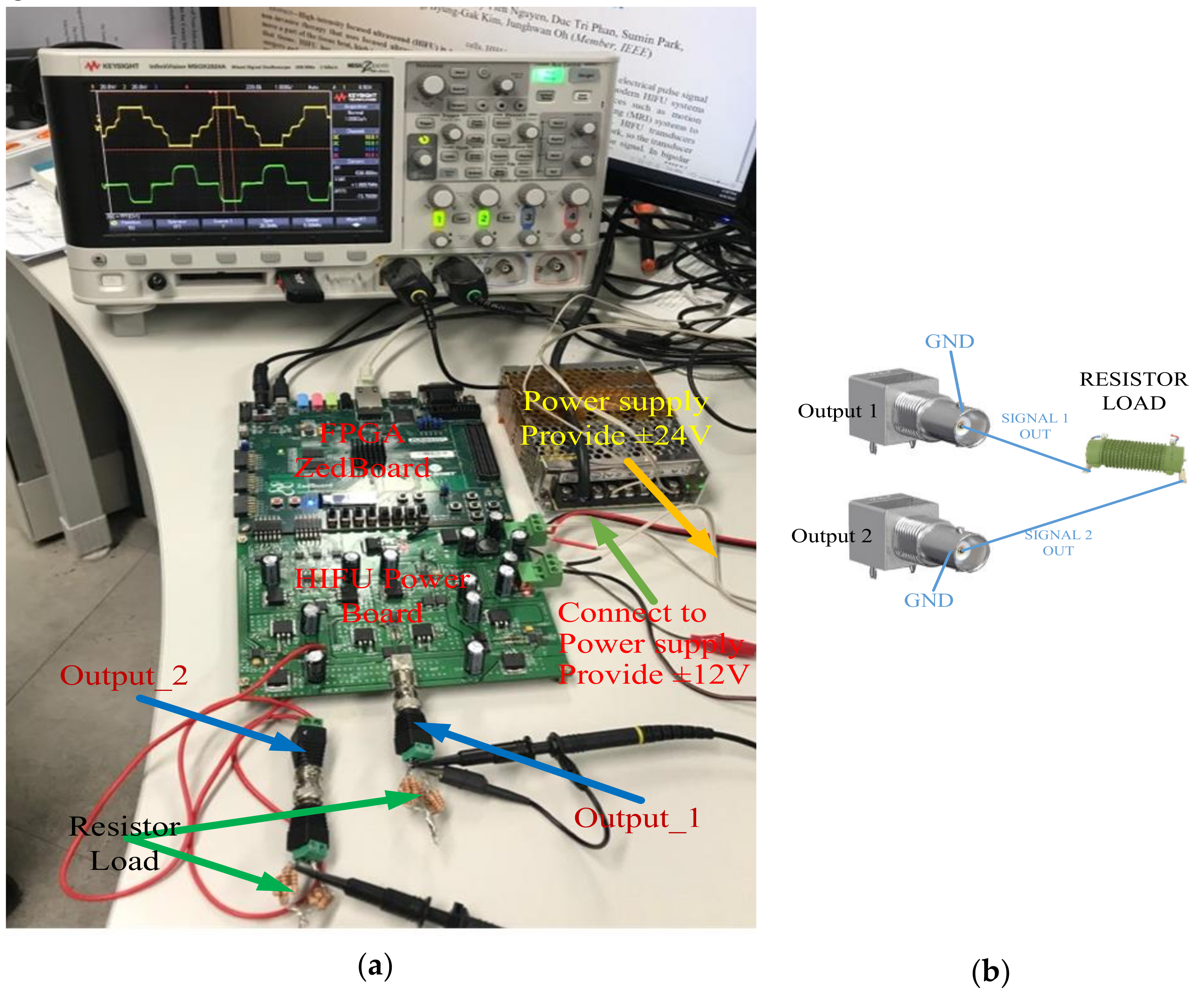
Figure 12.
(a) Setup of the HIFU system with the resistor load, (b) combination of two outputs of the HIFU signal generator circuit.
Figure 12.
(a) Setup of the HIFU system with the resistor load, (b) combination of two outputs of the HIFU signal generator circuit.
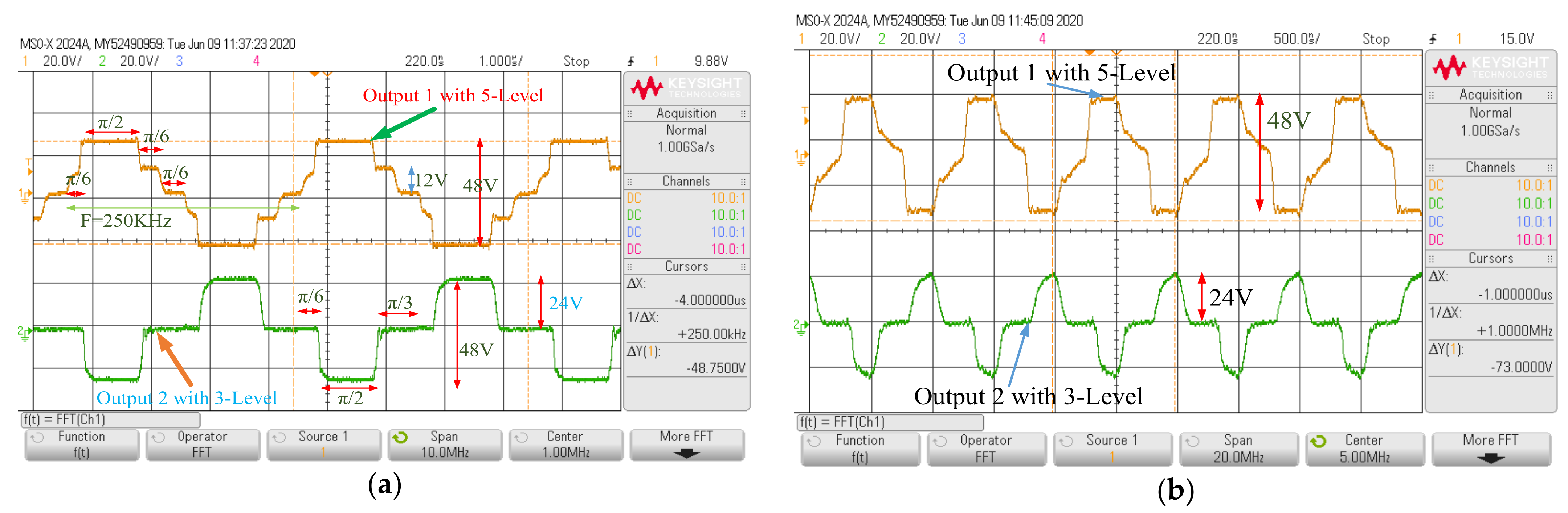
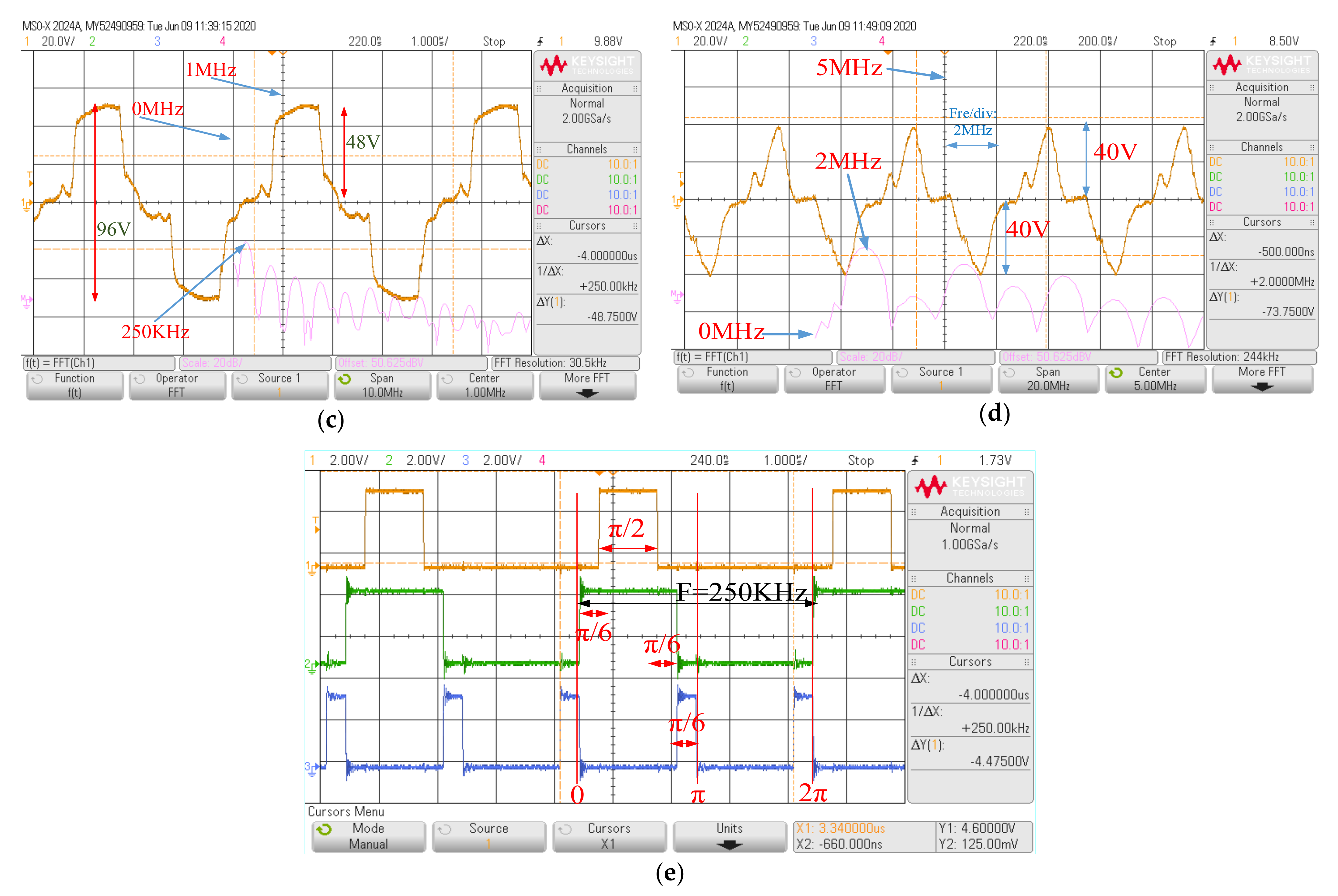
Figure 13.
The output signal of HIFU power board: single output at frequency (a) 250 kHz, (b) 1 MHz, two outputs become one output at frequency (c) 250 kHz, (d) 1 MHz, (e) signal control MOSFET pair from FPGA with a five-level signal output and a frequency at 250 kHz.
Figure 13.
The output signal of HIFU power board: single output at frequency (a) 250 kHz, (b) 1 MHz, two outputs become one output at frequency (c) 250 kHz, (d) 1 MHz, (e) signal control MOSFET pair from FPGA with a five-level signal output and a frequency at 250 kHz.
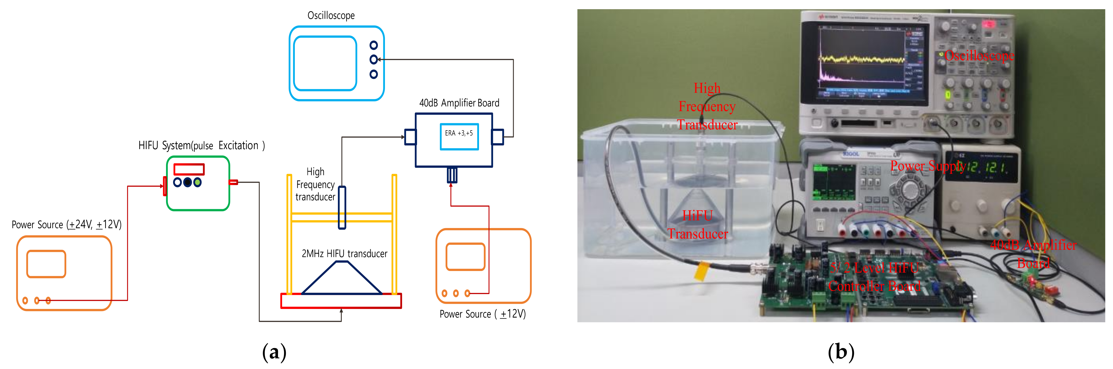
Figure 14.
(a) Block diagram of HIFU experiment system; (b) the real HIFU experiment system.
Figure 14.
(a) Block diagram of HIFU experiment system; (b) the real HIFU experiment system.
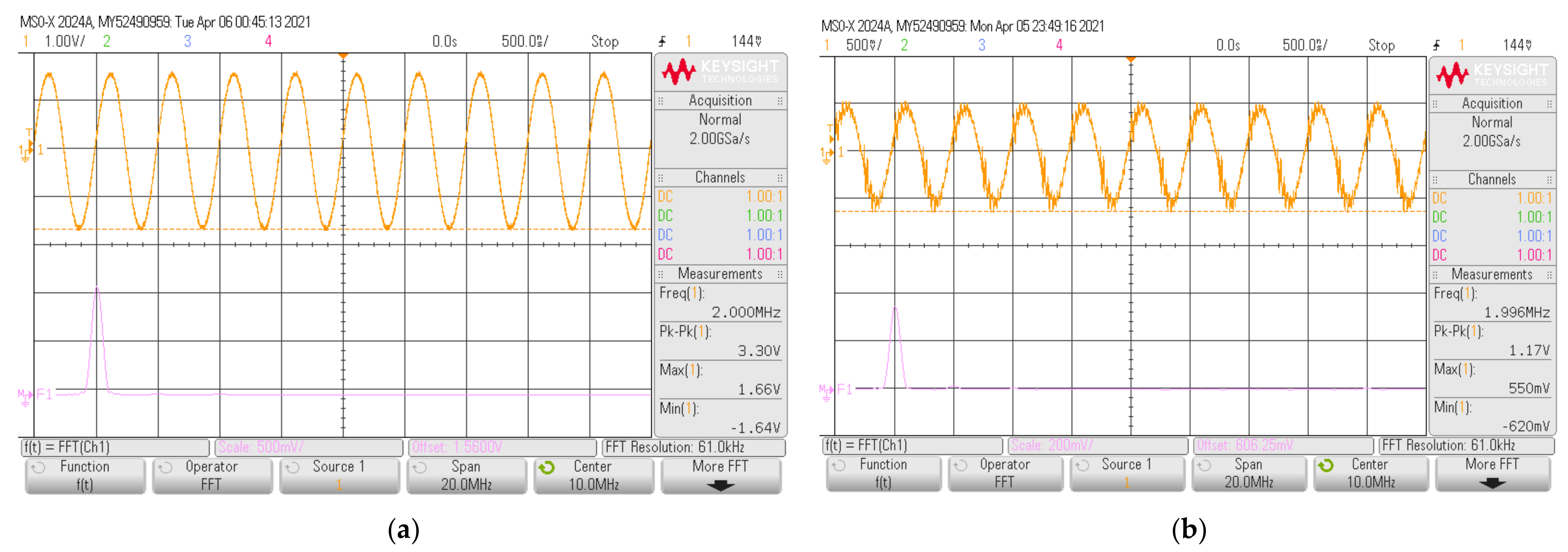
Figure 15.
Output signal from high frequency transducer with: (a) 5-level sine wave, (b) 2-level square wave for excitation 2 MHz HIFU transducer.
Figure 15.
Output signal from high frequency transducer with: (a) 5-level sine wave, (b) 2-level square wave for excitation 2 MHz HIFU transducer.
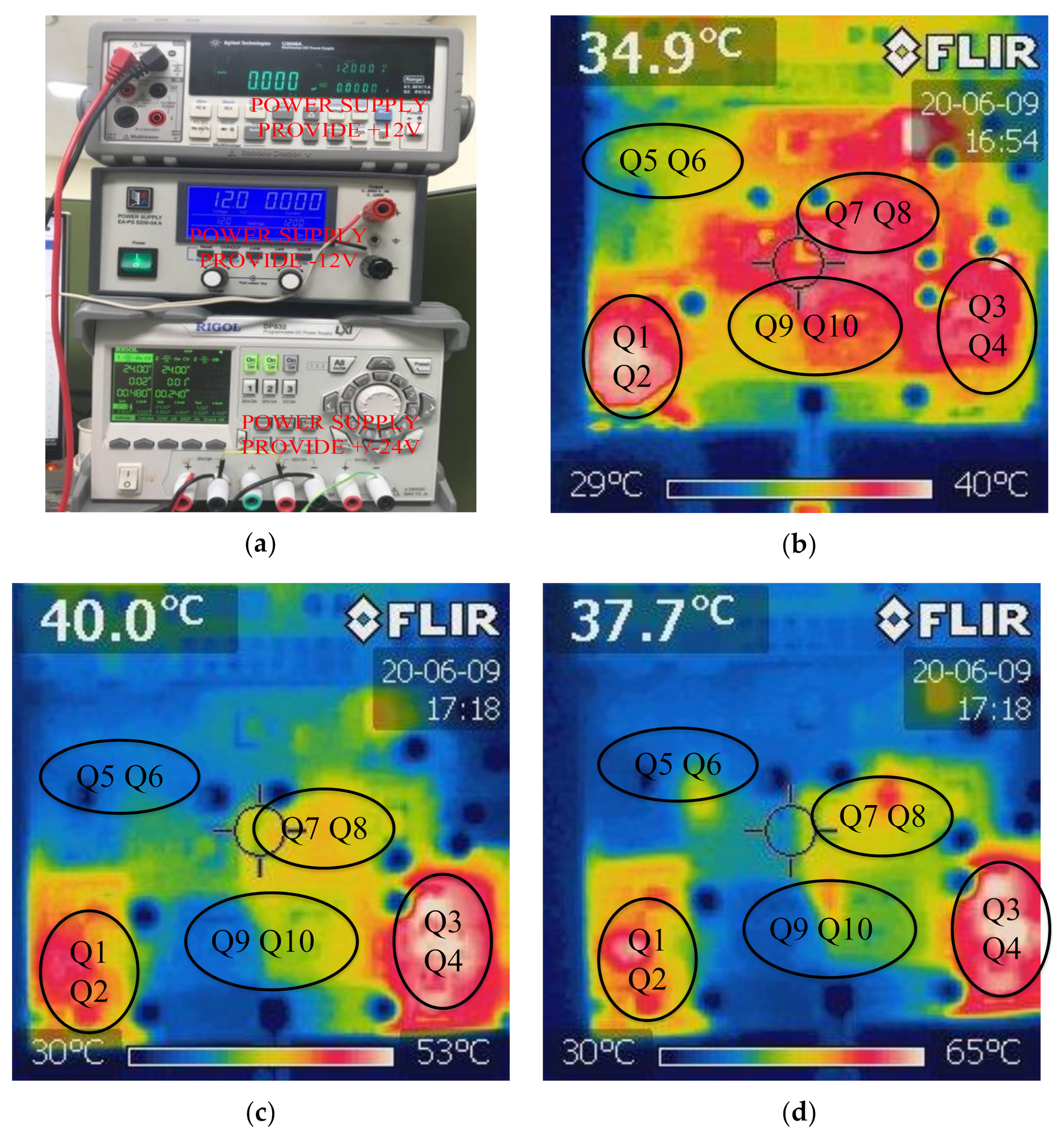
Figure 16.
Thermal dissipation of power MOSFETs on PCB with a combination of two outputs: (a) at frequency 250 kHz, (b) at frequency 1 MHz, and (c) at frequency 2 MHz, (d) at frequency 3 MHz.
Figure 16.
Thermal dissipation of power MOSFETs on PCB with a combination of two outputs: (a) at frequency 250 kHz, (b) at frequency 1 MHz, and (c) at frequency 2 MHz, (d) at frequency 3 MHz.
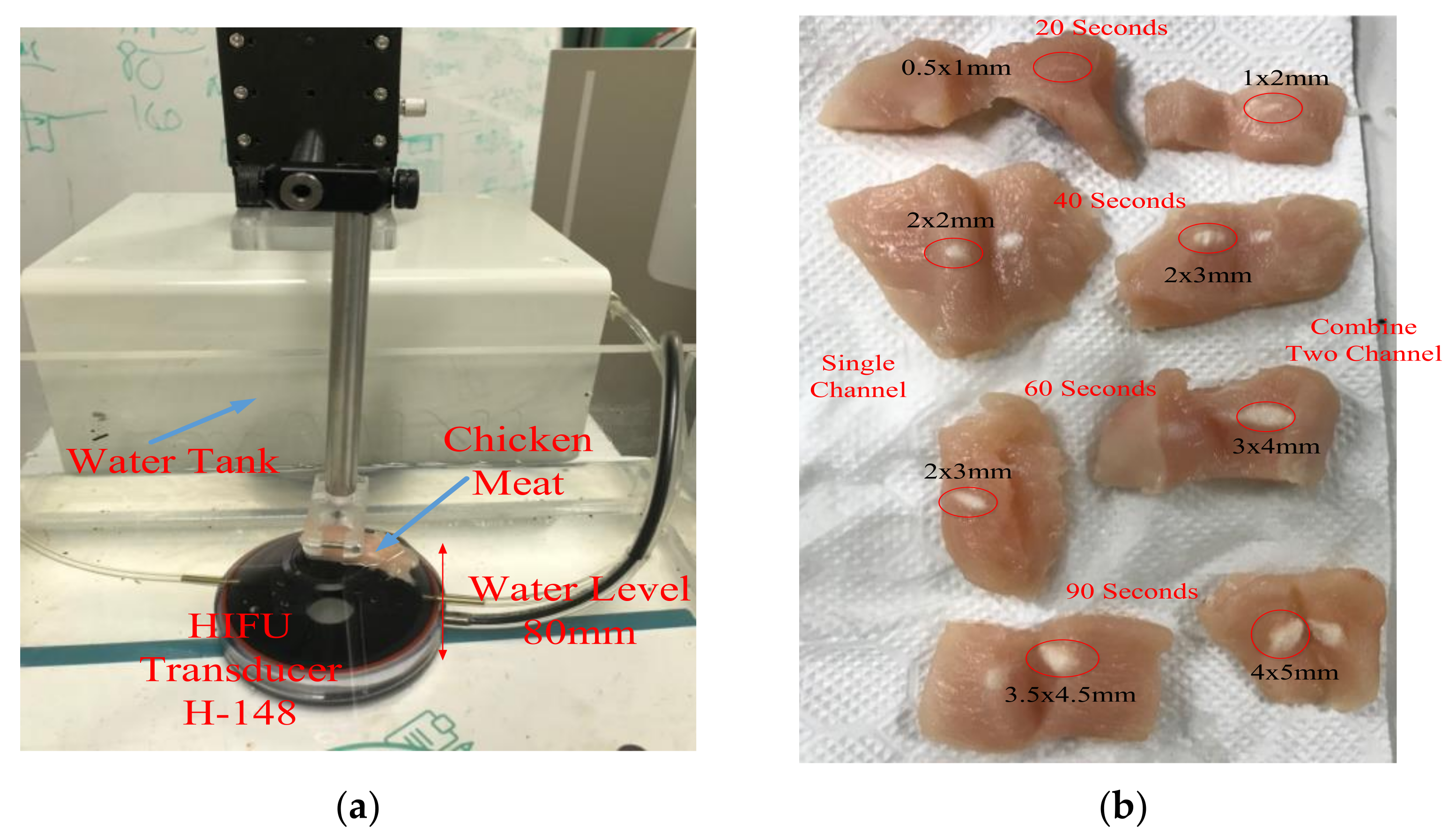
Figure 17.
(a) Setup of the HIFU transducer with chicken meat and a water tank, (b) comparison of the burned area of chicken meat, using the HIFU system with a different time between the single channel output and the combined two outputs.
Figure 17.
(a) Setup of the HIFU transducer with chicken meat and a water tank, (b) comparison of the burned area of chicken meat, using the HIFU system with a different time between the single channel output and the combined two outputs.
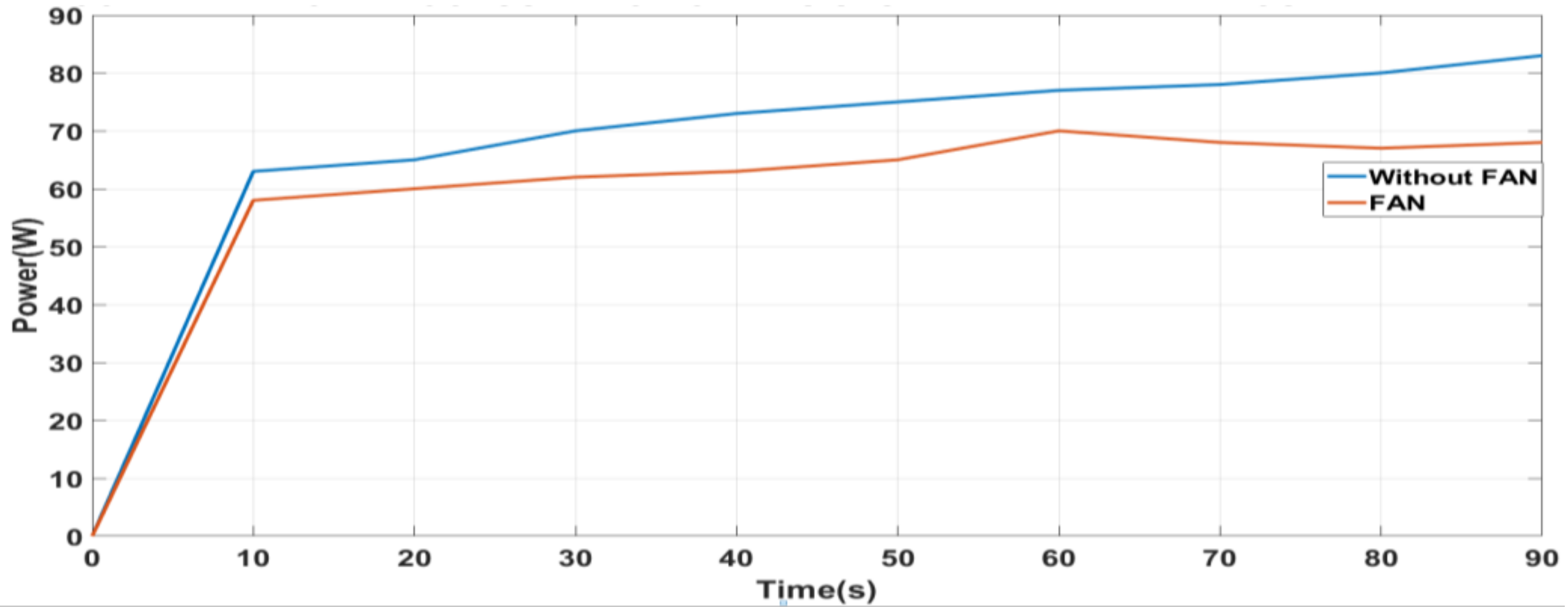
Figure 18.
Comparison of the power consumption of the HIFU system with and without the fan.
Figure 18.
Comparison of the power consumption of the HIFU system with and without the fan.
Table 1.
Typical thermal conductivities of FR-4 board layers including vias.
Table 1.
Typical thermal conductivities of FR-4 board layers including vias.
| Layer/Material | Thickness (µm) | Thermal Conductivity (W/(cm °C)) |
|---|
| Top layer copper | 35 | 3.98 |
| FR-4 | 1588 | 0.002 |
| Bottom layer copper | 35 | 3.98 |
| Solder mask | 25 | 0.002 |
Table 2.
Typical and maximum thermal resistance.
Table 2.
Typical and maximum thermal resistance.
| Package Type | Thermal Resistance (One Square Inch) |
|---|
| Typical (Rth(JA)) | Max (Rth(JA)) |
|---|
| D-Pak | 20.2 | 26.3 |
| D2-Pak | 18.8 | 23.3 |
| SO-8 | 33.5 | 50.0 |
| SOT-223 | 27.2 | 60 |
| TSSOP8 | 60.9 | 83.0 |
Table 3.
Parameters of IRF9540NS (To-263) [
35].
Table 3.
Parameters of IRF9540NS (To-263) [
35].
| Symbol | Parameter | Ratings |
|---|
| ID | Drain Current-Continuous (Max@TC = 25 °C) | −23 A |
| TJ | Operating Junction Temperature Range | −55 to 175 °C |
| RθJC | Thermal Resistance, Junction-to-Case | 1.1 °C/W |
| RDS(on) | Static Drain–Source On-Resistance (Max at TJ = 125 °C) | 117 mΩ |
| Crss | Reverse Transfer Capacitance | 240 pF |
| Qg | Total Gate Charge | 97 nC |
| VSD | Drain–Source Diode Forward Voltage | −1.6V |
Table 4.
Parameters of IRF540NS (To-263) [
36].
Table 4.
Parameters of IRF540NS (To-263) [
36].
| Symbol | Parameter | Ratings |
|---|
| ID | Drain Current-Continuous (Max@TC = 25 °C) | 33A |
| TJ | Operating Junction Temperature Range | −55 to 175 °C |
| RθJC | Thermal Resistance, Junction-to-Case | 1.15 °C/W |
| RDS(on) | Static Drain–Source On-Resistance (Max at TJ = 125 °C) | 44 mΩ |
| Crss | Reverse Transfer Capacitance | 40 pF |
| Qg | Total Gate Charge | 71 nC |
| VSD | Drain–Source Diode Forward Voltage | 1.2 V |
Table 5.
Power dissipated of IRF9540NS (TO-263).
Table 5.
Power dissipated of IRF9540NS (TO-263).
| Symbol | Ratings | PMOSFET | PDRIVER |
|---|
| ILOAD | 3 A | 10.84 W | 1.94 W |
| RDS(ON) | 117 mΩ |
| VIN | 48 V |
| FSW | 2 MHz |
| D | 0.5 |
| IGATE | 0.5 A |
| Crss | 240 pF |
| VSD | 1.6 V |
| QG | 97 nC |
Table 6.
Power dissipated of IRF540NS (TO-263).
Table 6.
Power dissipated of IRF540NS (TO-263).
| Symbol | Ratings | PMOSFET | PDRIVER |
|---|
| ILOAD | 3 A | 3.5 W | 1.42 W |
| RDS(ON) | 44 mΩ |
| VIN | 48 V |
| D | 0.5 |
| FSW | 2 MHz |
| IGATE | 0.5 A |
| Crss | 40 pF |
| D | 0.5 |
| VSD | 1.2 V |
| QG | 71 nC |
Table 7.
Copper area of PCB heat sink for TO-263.
Table 7.
Copper area of PCB heat sink for TO-263.
| Symbol | No of Vias | Top Area (cm2) | Bottom Area (cm2) |
|---|
| IRF9540NS | 20 | 3.5 | 3.5 |
| IRF540NS | 20 | 3.5 | 3.5 |
Table 8.
Copper area of PCB heat sink for TO-263 with different MOSFETs.
Table 8.
Copper area of PCB heat sink for TO-263 with different MOSFETs.
| Symbol | No. of Vias | Top Area (cm2) | Bottom Area (cm2) |
|---|
| IRF9540(Q1) | 32 | 3.84 | 4.6 |
| IRF540 (Q2) | 36 | 3.98 | 4.1 |
| IRF9540(Q3) | 21 | 3.5 | 5.4 |
| IRF540 (Q4) | 23 | 4.02 | 4.2 |
| IRF9540(Q5) | 34 | 3.63 | 5.1 |
| IRF540 (Q6) | 32 | 3.7 | 5.3 |
| IRF9540(Q7) | 18 | 2.2 | 5.7 |
| IRF540 (Q8) | 30 | 3.8 | 5.3 |
| IRF9540(Q9) | 24 | 3.39 | 4.9 |
| IRF540 (Q10) | 26 | 3.96 | 4.7 |
Table 9.
Power consumption on channel 1 with differences in voltage level.
Table 9.
Power consumption on channel 1 with differences in voltage level.
| | Power Consumption (W) |
|---|
| Frequency | +24 V | −24 V | +12 V | −12 V |
| 250 KHz | 9.5 | 8.2 | 2.8 | 1.6 |
| 1 MHz | 14.5 | 11 | 2.2 | 1.6 |
| 2 MHz | 17.5 | 13 | 1.4 | 1.3 |
| 3 MHz | 20.5 | 13.5 | 1.1 | 0.8 |
Table 10.
Combination of two-channel power consumption with differences in voltage level.
Table 10.
Combination of two-channel power consumption with differences in voltage level.
| | Power Consumption (W) |
|---|
| Frequency | +24 V | −24 V | +12 V | −12 V |
| 250 KHz | 15 | 12 | 2.8 | 1.6 |
| 1 MHz | 18 | 13 | 2.1 | 1.6 |
| 2 MHz | 21.5 | 15 | 1.2 | 1 |
| 3 MHz | 28.5 | 19 | 0.8 | 0.8 |
Table 11.
The comparison with previous research.
Table 11.
The comparison with previous research.
| | Our Design | Ref [39] | Ref [40] | Ref [9] |
|---|
| Frequency | 0.1→5 MHz | 2 MHz | 1.54 MHz | 1.1 MHz |
| Max Output Voltage (V) | ±48 | ±20 | ±12 | ± 12 |
| Max Output Power (W) | ≥100 | - | 50 | 35 |
| Shape of Ouput | Multi-level sinusoidal | Square | Square | Multi-level sinusoidal |


 ,
, 


