Article

Single Step 2-Port Device De-Embedding Algorithm for Fixture-DUT-Fixture Network Assembly

1
UAq EMC Laboratory, Department of Industrial and Information Engineering and Economics, University of L’Aquila, 64100 L’Aquila, Italy
2
Missouri S & T EMC Laboratory, Missouri University of Science and Technology, Rolla, MO 65409, USA
*
Author to whom correspondence should be addressed.
Electronics 2021, 10(11), 1275; https://doi.org/10.3390/electronics10111275
Submission received: 1 May 2021 / Revised: 18 May 2021 / Accepted: 25 May 2021 / Published: 27 May 2021

Abstract

:
The de-embedding of measurement fixtures is relevant for an accurate experimental characterization of radio frequency and digital electronic devices. The standard technique consists in removing the effects of the measurement fixtures by the calculation of the transfer scattering parameters (T-parameters) from the available measured (or simulated) global scattering parameters (S-parameters). The standard de-embedding is achieved by a multiple steps process, involving the S-to-T and subsequent T-to-S parameter conversion. In a typical measurement setup, two fixtures are usually placed before and after the device under test (DUT) allowing the connection of the device to the calibrated vector network analyzer coaxial ports. An alternative method is proposed in this paper: it is based on the newly developed multi-network cascading algorithm. The matrices involved in the fixture-DUT-fixture cascading gives rise to a non-linear set of equations that is in one step analytically solved in closed form, obtaining a unique solution. The method is shown to be effective and at least as accurate as the standard multi-step de-embedding one.

1. Introduction

The precise characterization and validation of electronics devices for radio frequency (RF) and high-speed digital applications relies on scattering parameters (S-parameters) measurements. A well-known preliminary step for an accurate measurement is the calibration of the vector network analyzer (VNA) which moves the reference planes from the VNA output ports (usually its connectors) to the end of the cables used for the VNA to the device under test (DUT) connection [1,2]. This procedure is sufficient as long as the DUT that needs to be measured can be accessed by the VNA cables through coaxial connectors that directly match the VNA cables’ impedance [3]. However, very often such coaxial access points are not directly available for complex devices, unless appropriate test fixtures are designed to make accessible the DUT through coaxial ports. This is the case concerning the characterization of on-wafer devices, integrated circuits and packages, single transistors, connectors for RF and high-speed digital applications, waveguide transitions and other complex structures [4]. In this case the de-embedding of the test fixtures (usually named “left” and “right” fixtures) need to be applied in order to extract the impact of their presence from the overall measured S-parameter. This is done knowing the S-parameter data of the single fixtures that are applied before and after the DUT [5,6,7,8,9]. Usually the well-known de-embedding process in frequency domain is based at least on three main conceptual steps: first, the conversion of the S-parameters in the transfer scattering parameters (T-parameters) [10], second the algebraic manipulation and inversion of the T-parameter matrices, and third the final T-to-S parameter transformation. It should be noted that when actually implemented each single step calls some others making the real implementation rather complex.
In this paper a sophisticated but more efficient single step de-embedding process is proposed to perform the de-embedding of both left and right fixtures of a 2-port system in only a single step through the solution of a linear system of equations, without the need for any matrix inversion involved in the aforementioned S-to-T and T-to-S parameter conversion that introduces the numerical error (typically O(N2) where N is the order of the matrix) due to the iterative process for the evaluation of the inverse [11]. Once implemented, the solution is applied directly on the raw measured S-parameters of the fixture-DUT-fixture system knowing those of each fixture without any conversion to T-parameters. The analytical solution is an extension of the algorithm developed for the cascading of two S-parameter blocks in [12]. The algorithm is expanded to the case of three blocks (or networks) representing the S-parameters of the left fixture (FL), of the DUT and of the right fixture (FR) based on the cascading of the S-parameter blocks network considered in [12]. The classical method for the cascading of two networks is here expanded to the case of three networks that are identified in the following as the left fixture (FL), the DUT, and the right fixture (FR). The direct solution of the three blocks cascading process gives rise, through few matrix-algebraic manipulations, to a set of four non-linear equations in four auxiliary unknowns that are directly and analytically related to the sought DUT S-parameters (SDUT1,1, SDUT1,2, SDUT2,1, SDUT2,2). This system of non-linear equations has a closed form solution clear of any numerical error.
It is used for building a linear set of four equations in five unknowns: the four unknowns of the DUT S-parameters (SDUT1,1, SDUT1,2, SDUT2,1, SDUT2,2) plus their combination coming out from the matrix determinant built along the cascading process. By means of a matrix-algebraic manipulation the problem is reduced to a set of four auxiliary equations in four unknowns and their solution used to find the valid and unique closed form solution of the DUT S-parameters.
The structure of the paper is the following: the S-parameter cascading of two two-port networks is briefly reviewed in Section 2, and it is expanded for the case of three two-port networks. Section 3 presents the analytical derivation of the method for the single-step fixture de-embedding. Section 4 provides some validation examples by comparing the original DUT S-parameters with those computed after applying the de-embedding developed here. Section 5 offers some concluding remarks.

2. S-Parameter Cascade of Three Networks

2.1. Review of Two-Network S-Parameter Cascading Algorithm

The two 2-port S-parameter networks FL and FR in Figure 1 are considered, whose S-parameters are defined by (1) and (2), respectively, and they are assumed to be known.
[ b F L , i b F L , o ] = [ S F L   1 , 1 S F L   1 , 2 S F L   2 , 1 S F L   2 , 2 ] [ a F L , i a F L , o ]
[ b F R , i b F R , o ] = [ S F R   1 , 1 S F R   1 , 2 S F R   2 , 1 S F R   2 , 2 ] [ a F R , i a F R , o ]
where aα,β and bα,β are the incident and reflected power waves respectively [10]. The subscript α = FL, FR denotes if the wave belongs to the FL or FR network; the subscript β = i,o identifies if the wave is at the input or output port of the network.
An overall S-parameters matrix that combines all elements of both networks can be written as:
[ b F L , i b F R , o b F L , o b F R , i ] = [ S F L   1 , 1 0 0 S F L   1 , 2 0 S F R   2 , 2 S F R   2 , 1 0 S F L   2 , 1 0 0 S F L   2 , 2 0 S F R   1 , 2 S F R   1 , 1 0 ] [ a F L , i a F R , o a F R , i a F L , o ]
A compact form of the vectors and matrix in (3) can be defined by naming external parameters (‘e’) the input waves of network FL and the output waves of networks FR, and internal parameters (‘i’) the output waves of network FL and the input waves of network FR, according to the order in which each single S-parameter is placed in the matrix in (3).
b ¯ e = [ b F L , i b F R , o   ]
b ¯ i = [ b F L , o b F R , i   ]
a ¯ e = [ a F L , i a F R , o   ]
a ¯ i = [ a F R , i a F L , o   ]
This leads us to write (3) as in (4e):
[ b ¯ e b ¯ i ] = [ S = e e S = e i S = i e S = i i ] [ a ¯ e a ¯ i ]
In (4e) and in the following the vector and matrix variables will be denoted by one ( b ¯ ) or two ( S = ) hats, respectively.
At the boundary between the two networks, the waves must be continuous. In other words, the condition (5) applies:
b ¯ i = a ¯ i
By enforcing this continuity condition, one can obtain the expression of the total scattering parameters STOT in (6) from the external end ports FLi and FRo of the cascaded FL and FR networks.
S = T O T = S = e e + S = e i ( I = d S = i i ) 1 S = i e
where I = d is the identity matrix with the same size of S = i i .

2.2. Single Step S-Parameter Cascading Algorithm for Three 2-Port Networks

The process described above in (1)–(6) is extended to the case of interest based on the three 2-port networks in Figure 2. Since this configuration is preparatory for the de-embedding technique, the three networks are identified as FL, FR and DUT placed in between.
The S-parameters associated to each of these networks are given by (1) for FL, by (2) for FR and by (7) for the DUT.
[ b D U T , i b D U T , o ] = [ S D U T   1 , 1 S D U T   1 , 2 S D U T   2 , 1 S D U T   2 , 2 ] [ a D U T , i a D U T , o ]
As done in (3) for the simple case of two networks, the S-parameters of the three networks in Figure 2 can be arranged into a single matrix. This is done in (8) where the four S-parameter elements of the three networks are arranged such that the same boundary conditions in (5) apply.
[ b F L , i b F R , o b F L , o b D U T , i b D U T , o b F R , i ] = [ S F L   1 , 1 0 0 S F L   1 , 2 0 0 0 S F R   2 , 2 0 0 S F R   2 , 1 0 S F L   2 , 1 0 0 S F L   2 , 2 0 0 0 0 S D U T   1 , 1 0 0 S D U T   1 , 2 0 0 S D U T   2 , 1 0 0 S D U T   2 , 2 0 S F R   1 , 2 0 0 S F R   1 , 1 0 ] [ a F L , i a F R , o a D U T , i a F L , o a F R , i a D U T , o ]
In order to map (8) into (4), the size of the sub-matrices defined in (4) will be the following: 2 × 2 for the S = e , e , 2 × 4 for the S = e , i , 4 × 2 for the S = i , e , and 4 × 4 for the S = i , i . This matrix arrangement will make possible a direct calculation of the cascaded S-parameters according to (6), with S = T O T   representing the S-parameters between the external end ports FLi and FRo in Figure 2.

3. Single-Step Algorithm for Device under Test (DUT) De-Embedding

The S-parameter matrix equation in (6) is written in different form as in (9):
  S ¯ ¯ T O T S ¯ ¯ e e = S ¯ ¯ e i ( I d ¯ ¯ S ¯ ¯ i i ) 1 S ¯ ¯ i e
It gives rise to a set of four non-linear equations as explicitly written in (10):
{ S T O T 1 , 1     S F L 1 , 1 + S F L 1 , 2   S F L 2 , 1 S D U T 1 , 1 + S F L 1 , 2   S F L 2 , 1 S F R 1 , 1 ( S D U T 1 , 2     S D U T 2 , 1   S D U T 1 , 1   S D U T 2 , 2 ) ( S F R 1 , 1   S D U T 2 , 2   +   S F L 2 , 2   S D U T 1 , 1 +   S F R 1 , 1 S F L 2 , 2 ( S D U T 1 , 2     S D U T 2 , 1   S D U T 1 , 1   S D U T 2 , 2 )     1 ) = 0 S T O T 1 , 2 + S F L 1 , 2 S F R 1 , 2 S D U T 1 , 2 ( S F R 1 , 1   S D U T 2 , 2   +   S F L 2 , 2   S D U T 1 , 1 +   S F R 1 , 1 S F L 2 , 2 ( S D U T 1 , 2     S D U T 2 , 1   S D U T 1 , 1   S D U T 2 , 2 )     1 ) = 0 S T O T 2 , 1 + S F L 2 , 1 S F R 2 , 1 S D U T 2 , 1 ( S F R 1 , 1   S D U T 2 , 2   +   S F L 2 , 2   S D U T 1 , 1 +   S F R 1 , 1 S F L 2 , 2 ( S D U T 1 , 2     S D U T 2 , 1   S D U T 1 , 1   S D U T 2 , 2 )     1 )     = 0 S T O T 2 , 2     S F R 2 , 2 + S F R 1 , 2 S F R 2 , 1 S D U T 2 , 2 + S F R 1 , 2 S F R 2 , 1 S F L 2 , 2 ( S D U T 1 , 2     S D U T 2 , 1   S D U T 1 , 1   S D U T 2 , 2 ) ( S F R 1 , 1   S D U T 2 , 2   +   S F L 2 , 2   S D U T 1 , 1 +   S F R 1 , 1 S F L 2 , 2 ( S D U T 1 , 2     S D U T 2 , 1   S D U T 1 , 1   S D U T 2 , 2 )     1 ) = 0
The system of equations in (10) involves the variables S D U T 1 , 1 , S D U T 1 , 2 , S D U T 2 , 1 S D U T 2 , 2 that represent the target unknown S-parameters of the DUT that should be computed. For the sake of convenience, the following equalities can be adopted:
Y ( 1 ) = S D U T 1 , 1
Y ( 2 ) = S D U T 1 , 2
Y ( 3 ) = S D U T 2 , 1
Y ( 4 ) = S D U T 2 , 2
C = S D U T 1 , 2     S D U T 2 , 1   S D U T 1 , 1   S D U T 2 , 2
Using these notations, the system in (10) becomes equal to the non-linear system in (12):
{ S T O T 1 , 1     S F L 1 , 1 + S F L 1 , 2   S F L 2 , 1 Y ( 1 ) + S F L 1 , 2   S F L 2 , 1 S F R 1 , 1 C ( S F R 1 , 1   Y ( 4 ) +   S F L 2 , 2   Y ( 1 ) +   S F R 1 , 1 S F L 2 , 2 C     1 ) = 0 S T O T 1 , 2 + S F L 1 , 2 S F R 1 , 2 Y ( 2 ) ( S F R 1 , 1   Y ( 4 ) +   S F L 2 , 2   Y ( 1 ) +   S F R 1 , 1 S F L 2 , 2 C     1 ) = 0 S T O T 2 , 1 + S F L 2 , 1 S F R 2 , 1 Y ( 3 ) ( S F R 1 , 1   Y ( 4 ) +   S F L 2 , 2   Y ( 1 ) +   S F R 1 , 1 S F L 2 , 2 C     1 )     = 0 S T O T 2 , 2     S F R 2 , 2 + S F R 1 , 2 S F R 2 , 1 Y ( 4 ) + S F R 1 , 2 S F R 2 , 1 S F L 2 , 2 C ( S F R 1 , 1   Y ( 4 ) +   S F L 2 , 2   Y ( 1 ) +   S F R 1 , 1 S F L 2 , 2 C     1 ) = 0
Finally, posing S S 1 = S T O T 1 , 1     S F L 1 , 1 and S S 2 = S T O T 2 , 2     S F R 2 , 2 , (12) can be rewritten as:
[ S S 1   S F L 2 , 2 + S F L 1 , 2   S F L 2 , 1 0 0 S S 1   S F R 1 , 1 S F L 2 , 2   S T O T 2 , 1 S F L 1 , 2 S F R 1 , 2 0 S F R 1 , 1   S T O T 2 , 1 S F L 2 , 2 S T O T 1 , 2 0 S F L 2 , 1 S F R 2 , 1 S F R 1 , 1 S T O T 1 , 2 S S 2   S F L 2 , 2 0 0 S S 2 S F R 1 , 1   + S F R 1 , 2 S F R 2 , 1 ] [ Y ( 1 ) Y ( 2 ) Y ( 3 ) Y ( 4 ) ] = [ (     S S 1   S F R 1 , 1 S F L 2 , 2 + S F L 1 , 2   S F L 2 , 1   S F R 1 , 1 ) C +   S S 1 S F R 1 , 1 S F L 2 , 2 S T O T 2 , 1 C +   S T O T 2 , 1   S F R 1 , 1 S F L 2 , 2 S T O T 1 , 2 C   +   S T O T 1 , 2 (   S S 2 S F R 1 , 1 S F L 2 , 2   +   S F R 1 , 2 S F R 2 , 1 S F L 2 , 2 ) C +   S S 2 ]
That in compact form is equivalent to (14):
A Y = B
All components of the solution are linearly dependent on C . The solution of the non-linear equation system in (13) can be achieved by a two step process: first, the linear system (13) can be solved first as function of the parameter C , and then the non-linear equation in (11e) can be solved. By assuming that the matrix A is not singular, the unique solution of the linear system depending on C is given by (15):
Y ¯ = S F L 1 , 2 S F R 1 , 2 S F L 2 , 1 S F R 2 , 1 d e t ( A ) · [ ( ( S F R 1 , 1 2 S F L 1 , 2 S F L 2 , 1 S T O T 2 , 2 S F R 1 , 1 2 S F L 1 , 2 S F L 2 , 1 S F R 2 , 2 +   S F R 1 , 1 S F L 1 , 2 S F R 1 , 2 S F L 2 , 1 S F R 2 , 1 ) C   ( S F L 1 , 1 S F R 1 , 2 S F R 2 , 1   S F R 1 , 2 S F R 2 , 1 S T O T 1 , 1 ) ) S F L 2 , 1 S F R 2 , 1 S T O T 1 , 2 ( S F R 1 , 1 S F L 2 , 2 C + 1 ) S F L 1 , 2 S F R 1 , 2 S T O T 2 , 1 ( S F R 1 , 1 S F L 2 , 2 C +   1 ) ( ( S F L 1 , 1 2 S F R 1 , 2 S F R 2 , 1 S T O T 1 , 1 S F L 2 , 2 2 S F R 1 , 2 S F R 2 , 1 S F L 1 , 1 +   S F L 1 , 2 S F R 1 , 2 S F L 2 , 1 S F R 2 , 1 S F L 2 , 2 ) C   ( S F L 1 , 1 S F L 1 , 2 S F R 2 , 2   S F L 1 , 2 S F L 2 , 1 S T O T 2 , 2 ) ) ]
where d e t ( A ) is the determinant of the matrix A in (14) given by:
d e t ( A ) = S F L 2 , 1 S F R 2 , 1 S F L 1 , 2 S F R 1 , 2 · [ ( S S 1   S F L 2 , 2 + S F L 1 , 2   S F L 2 , 1 ) ( S S 2 S F R 1 , 1   + S F R 1 , 2 S F R 2 , 1 ) S S 1   S S 2   S F R 1 , 1 S F L 2 , 2 ]
By replacing the solutions (15) into (11e) a second degree equation is obtained, whose roots are given by:
{ λ 1 = 1 S F R 1 , 1 S F L 2 , 2 λ 2 = S F L 1 , 1 S T O T 2 , 2   S F L 1 , 1 S F R 2 , 2 +   S F R 2 , 2 S T O T 1 , 1   S T O T 1 , 1 S T O T 2 , 2 +   S T O T 1 , 2 S T O T 2 , 1 A A
A A = ( S F L 1 , 1 S F L 2 , 2   S F L 1 , 2 S F L 2 , 1   S F L 2 , 2 S T O T 1 , 1 ) · ( S F R 1 , 1 S F R 2 , 2   S F R 1 , 2 S F R 2 , 1 S F R 1 , 1 S T O T 2 , 2 )   S F L 2 , 2 S F R 1 , 1 S T O T 1 , 2 S T O T 2 , 1
According to (17) two separate solutions of the non-linear system (12) should be found, Y ¯ 1 and Y ¯ 2 coming from λ 1 and λ 2 in (17), respectively. However, the solution Y 1 is not acceptable since the determinant of the matrix to be inverted in (9) is always zero, as in (19).
d e t ( I S D U T ) = ( S F R 1 , 1 Y 1 ( 4 ) +   S F L 2 , 2 Y 1 ( 1 ) +   S F R 1 , 1 S F L 2 , 2 λ 1   1 ) = 0
Therefore, the only and unique solution to the problem in (12) is given by Y 2 in (20),
Y ¯ 2   = 1 A A [ ( S T O T 1 , 1 S F L 1 , 1 ) ( S F R 1 , 2 S F R 2 , 1   S F R 1 , 1 S F R 2 , 2 +   S F R 1 , 1 S T O T 2 , 2 )   S F R 1 , 1 S T O T 1 , 2 S T O T 2 , 1 S F L 2 , 1 S F R 2 , 1 S T O T 1 , 2 S F L 1 , 2 S F R 1 , 2 S T O T 2 , 1 ( S T O T 2 , 2 S F R 2 , 2 ) ( S F L 1 , 2 S F L 2 , 1 S F L 2 , 2 S F L 1 , 1 +   S F L 2 , 2 S T O T 1 , 1 )   S F L 2 , 2 S T O T 1 , 2 S T O T 2 , 1 ]    
where the scalar variable AA in the denominator of (20) is given by the expression in (18). Y ¯ 2 is a vector containing the elements from (11a)–(11d), that is to say, the wanted S-parameters of the DUT that need to be computed at the end of the de-embedding process. Please note as the entries of Y ¯ 2 are the basic algebraic operations applied to the scattering parameters of the total system (feature-DUT-feature) and of the left and right feature.

4. Validation of the Proposed Single-Step De-Embedding

The single step de-embedding process described in Section 3 is implemented and validated in this Section based on a practical example of a multi-pin connector model suitable for a non-return to zero (NRZ) bit-rate up to 56 Gbps. The NRZ coding is often used for data signaling in telecommunications.
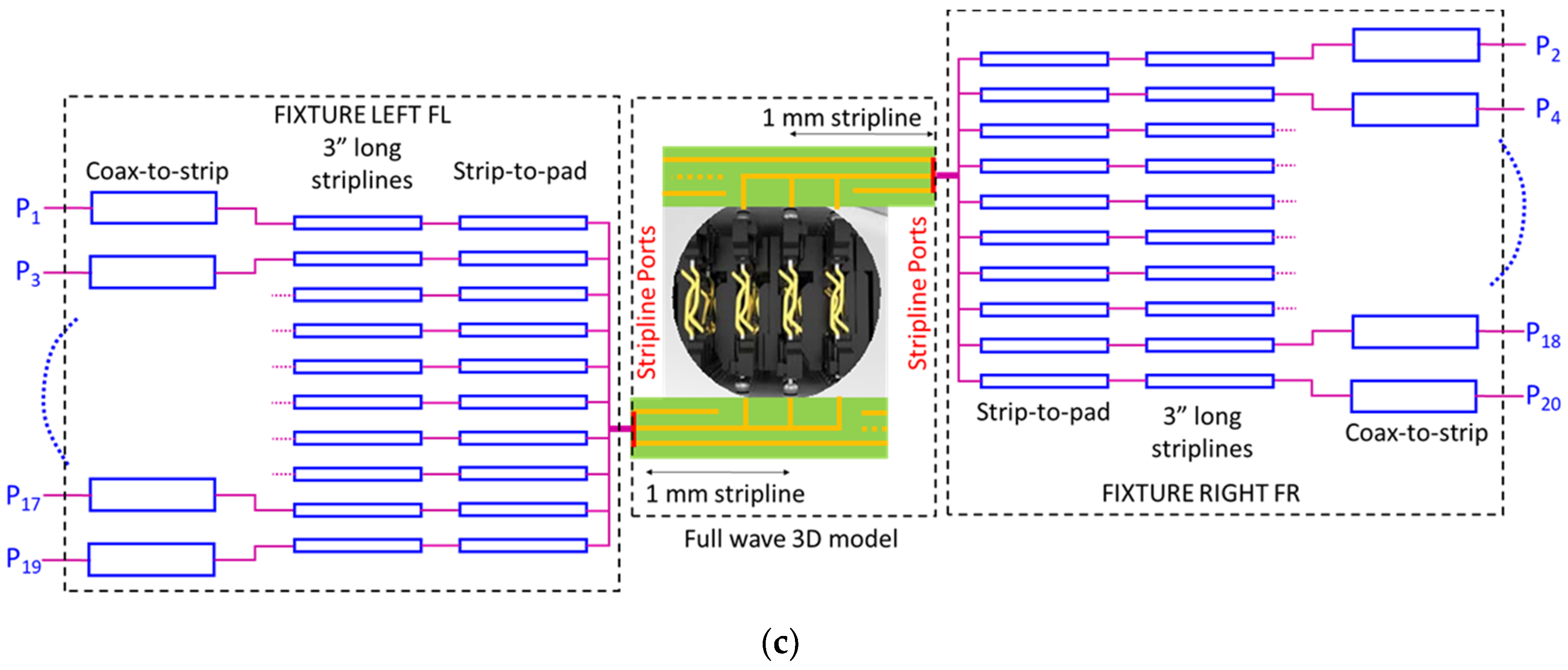
The connector itself, the DUT in Figure 3a,b, is described in [13], developed in the form of a full wave three-dimensional model by SAMTEC [14], and its S-parameters evaluated up to 50 GHz. The S-parameters and the equivalent circuit of the left (FL) and right (FR) fixtures in Figure 3b,c. have been derived in [15]. Based on [15], a single-ended line of the stand-alone connector model is extracted from the multiport S-parameters, and it is embedded in between the corresponding single-ended circuit models of the fixture according to Figure 3a. A more detailed description of the FL and FR fixtures is provided in Figure 3b,c. The S-parameters STOT from Port 1 to Port 2 in Figure 3a have been measured in [15] up to 50 GHz. All the four blocks of S-parameters (for the original DUT, for the two fixtures and for the entire system from Port 1 to Port 2) in this work have been considered as input data for this work.
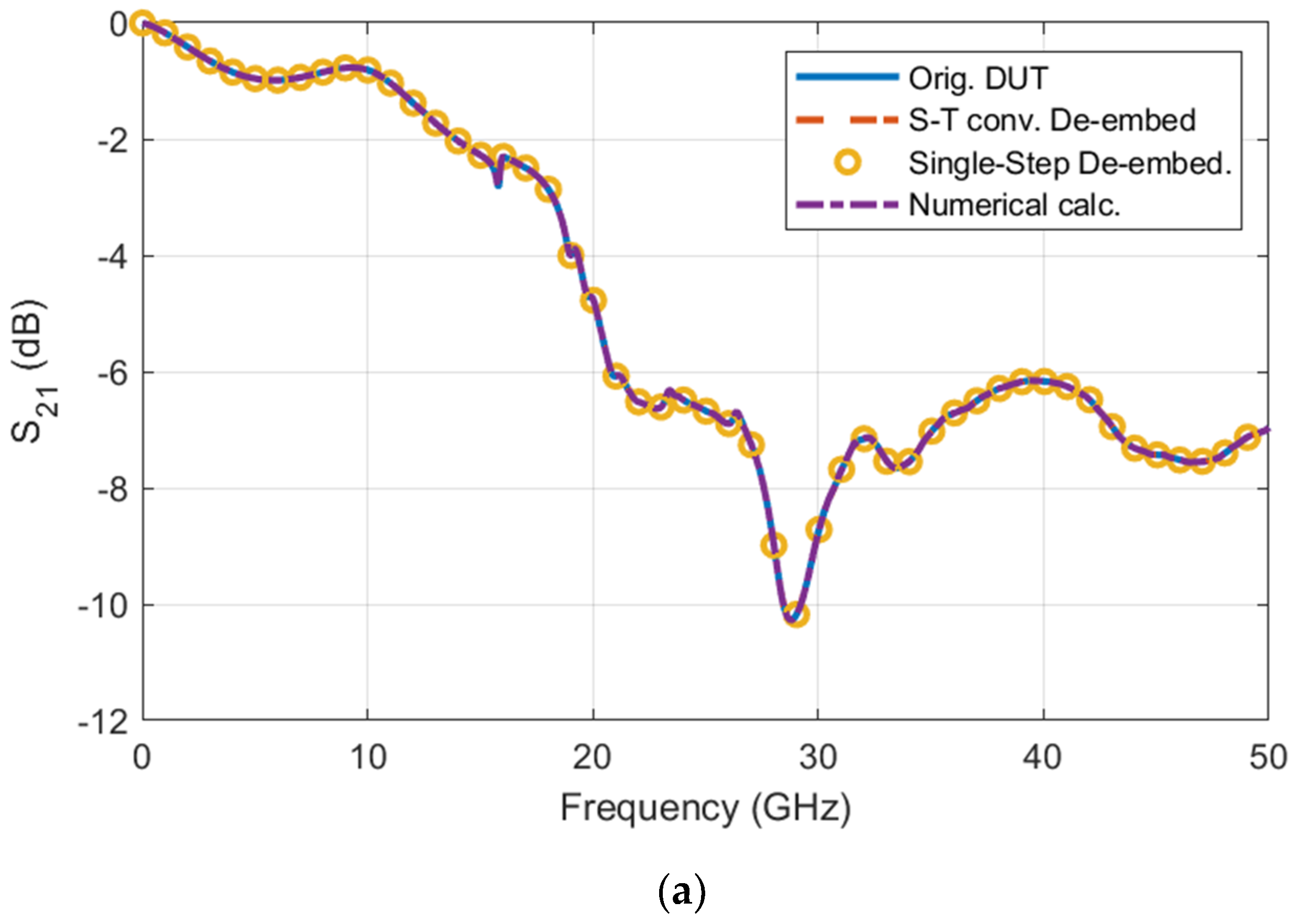
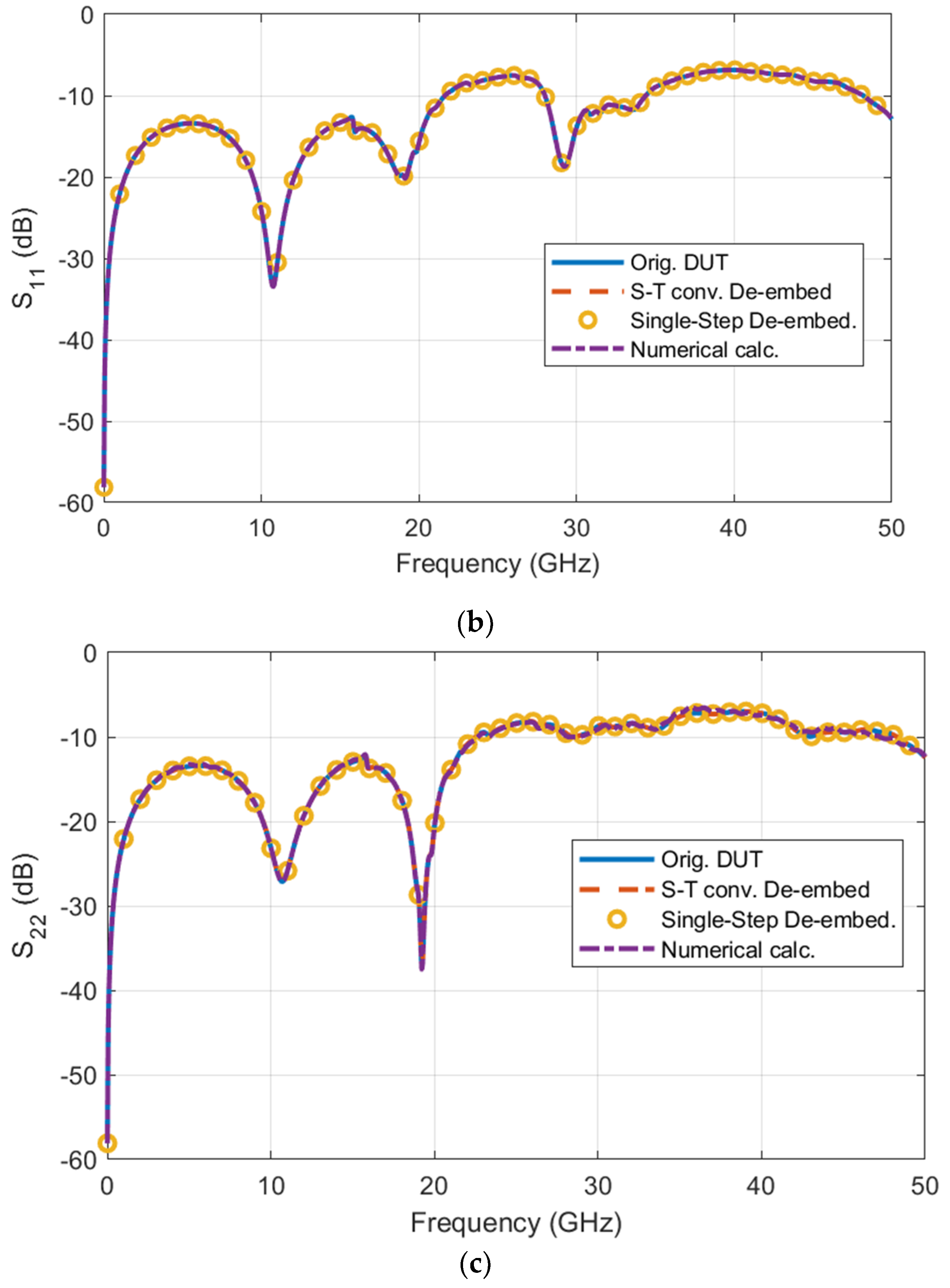
The validation of the single-step procedure consists in finding the S parameters of the DUT (the vector Y2 from (20)) from the knowledge of STOT (from Port 1 to Port 2 in Figure 3a) and comparing them with other independent solutions. The de-embedded DUT S-parameters from (20) (named “Single-Step De-Embed.” in Figure 4) are compared:
  • to those of the standalone original DUT known by measurement and modeling as shown in [15] and considered as reference result. They are named “Orig. DUT” in Figure 4;
  • to those obtained by applying the classic standard two-step S-to-T and T-to-S parameter conversion named “S-T conv. De-embedding” in Figure 4;
  • to those computed by applying a numerical iterative solution to the non-linear set of equations in (13) based on the MATLAB built in function fsolve [16] named “Numerical calc.” in Figure 4.
The overall comparisons of the obtained DUT S-parameters S21, S11, and S22 are reported in Figure 4.
By starting with a simple visual inspection of Figure 4 it is evident that the accuracy of the solution in (20) is good. In order to better quantify the differences of the S-parameters of the DUT obtained after de-embedding by the different approaches with respect to those of the standalone original DUT considered as reference, Table 1 and Table 2 have been compiled. In Table 1 each entry of the Table represents the maximum value of the magnitude of the difference (or maximum absolute error) between the Sij by each method and the same S-parameter of the standalone original DUT.
In Table 2 each entry of the Table represents the root mean squared difference between the Sij by each method and the same S-parameter of the standalone original DUT.
The results in Table 1 and Table 2 confirm the high level of accuracy of the single-step de-embedding procedure and show some weakness on the direct numerical solution of the non-linear system (13) especially for the S22 parameter whose error, although small, is not acceptable, since it is only one order of magnitude smaller than its absolute value. Both tables also intend to show that, from the accuracy point of view, the single step method is as accurate as the standard one performed in multiple steps. The main advantages of the new algorithm can be summarized as: (1) it uses a closed form solution without any approximation or inherent numerical error; (2) it is performed in one step so it is about 3× faster than the classic one: given the normalized execution time of the classic standard de-embedding procedure is 1, the normalized execution time of the single step procedure is 0.333 on the same hardware platform. This latter feature is very important when the de-embedding procedure should be repeated several times, as there are many frequencies of the spectrum of the sought DUT scattering parameters (usually several thousands).

5. Conclusions

A complete closed form method is proposed in this paper to de-embed the side fixtures within the three network fixture-DUT-fixture system typically encountered in the experimental setups for RF and digital device characterization. The method can be readily implemented and provides the DUT S-parameters in a single calculation step, without relying on the S-to-T parameter conversion typical of the classic de-embedding procedure. Furthermore, this standard procedure is applied in three steps, to remove the effect of left and right fixtures separately.
The method is instead a single-step process in which the final results are obtained just calculating the entries of the vector Y ¯ 2 in (20); it is developed based on the direct solution in closed form of a non-linear system of equations in which it is identified as the valid and unique solution. The proposed de-embedding technique is demonstrated as accurate as the standard de-embedding, more accurate of the numerical solution attempted on the original non-linear system mentioned above, and faster than the standard one. Equation (3) is scalable, and can be extended not only to more blocks but also to blocks with a higher number of input and output ports. This is the aim of future research actions.
The proposed method can be further extended to the more general cases of higher port count rather than the simple two-port network systems.

Author Contributions

Conceptualization, E.P., F.d.P., J.D., A.O.; methodology, S.S., F.d.P., C.O., A.O.; software, S.S., F.d.P.; validation, S.S., F.d.P.; writing—original draft preparation, F.d.P.; writing—review and editing, A.O. All authors have read and agreed to the published version of the manuscript.

Funding

This research received no external funding.

Acknowledgments

The authors would like to thank Matthew Burns and Richard Mellitz at Samtec for providing the NovaRay Evaluation kit and the connector S-parameters from the full-wave model simulation, and Mike Resso, O.J. Danzy, and Tim Wang-Lee at Keysight Technologies for their insightful discussions.

Conflicts of Interest

The authors declare no conflict of interest.

References

  1. Stenarson, J.; Yhland, K. An overview of VNA calibration and uncertainty evaluation techniques. Ger. Microw. Conf. 2008, 1, 1–4. [Google Scholar]
  2. Stumper, U. Uncertainties of VNA S-Parameter Measurements Applying the TAN Self-Calibration Method. IEEE Trans. Instrum. Meas. 2007, 56, 597–600. [Google Scholar] [CrossRef]
  3. Liu, Y.; Yong, S.; Gao, H.; Hinaga, S.; Padilla, D.; Yanagawa, D.; Drewniak, J.L.; Khilkevich, V. S-Parameter De-Embedding Error Estimation Based on the Statistical Circuit Models of Fixtures. IEEE Trans. Electromagn. Compat. 2020, 62, 1459–1467. [Google Scholar] [CrossRef]
  4. De Paulis, F.; Piersanti, S.; Wang, Q.; Cho, J.; Erickson, N.; Achkir, B.; Fan, J.; Drewniak, J.; Orlandi, A. TEM-Like Launch Geometries and Simplified De-embedding for Accurate Through Silicon Via Characterization. IEEE Trans. Instrum. Meas. 2017, 66, 792–801. [Google Scholar] [CrossRef]
  5. Resso, M.; Bogatin, E.; Vatsyayan, A. A new method to verify the accuracy of de-embedding algorithms. In Proceedings of the 2016 IEEE MTT-S Latin America Microwave Conference (LAMC), Puerto Vallarta, Mexico, 12–14 December 2016. [Google Scholar]
  6. Salnikov, A.S.; Dobush, I.M.; Bilevich, D.V.; Popov, A.A.; Kalentyev, A.A.; Goryainov, A.E. A Study of Connectors and Feed Lines De-Embedding Techniques for PCB Microwave Components S-Parameters Measurements Up To 50 Ghz. In Proceedings of the 2020 Dynamics of Systems, Mechanisms and Machines (Dynamics), Omsk, Russia, 10–12 November 2020. [Google Scholar]
  7. Chen, B.; Ye, X.; Samaras, B.; Fan, J. A novel de-embedding method suitable for transmission-line measurement. In Proceedings of the 2015 Asia-Pacific Symposium on Electromagnetic Compatibility (APEMC), Taipei, Taiwan, 25–29 May2015. [Google Scholar]
  8. Barnes, H.; Bogatin, E.; Moreira, J. Development of a PCB kit for s-parameter de-embedding algorithms verification. In Proceedings of the 2017 IEEE International Symposium on Electromagnetic Compatibility & Signal/Power Integrity (EMCSI), Washington, DC, USA, 7–11 August 2017. [Google Scholar]
  9. Cho, H.; Burk, D. A three-step method for the de-embedding of high-frequency S-parameter measurements. IEEE Trans. Electron Devices 1991, 38, 1371–1375. [Google Scholar] [CrossRef]
  10. Mavaddat, R. Network Scattering Parameters; World Scientific: Jefferson, NJ, USA, 1996. [Google Scholar]
  11. Sadiku, M.N.O. Numerical Techniques in Electromagnetics, 2nd ed.; CRC: New York, NY, USA, 2000. [Google Scholar]
  12. De Paulis, F.; Zhang, Y.-J.; Fan, J. Signal/Power Integrity Analysis for Multilayer Printed Circuit Boards Using Cascaded S-Parameters. IEEE Trans. Electromagn. Compat. 2010, 52, 1008–1018. [Google Scholar] [CrossRef]
  13. De Paulis, F.; Wang-Lee, T.; Mellitz, R.; Resso, M.; Rabinovich, R.; Danzy, O.J. Backplane channel design exploration at 112 Gbps using channel operating margin (COM). In Proceedings of the 2020 IEEE International Symposium on Electromagnetic Compatibility & Signal/Power Integrity (EMCSI), Reno, NJ, USA, 28 July–28 August 2020. [Google Scholar]
  14. SAMTEC. Available online: https://www.samtec.com/connectors/high-speed-board-to-board/high-density-arrays/novaray (accessed on 18 May 2021).
  15. De Paulis, F.; Wang-Lee, T.; Resso, M.; Mellitz, R.; Rabinovich, R.; Danzy, O. Validation and Performance Evaluation of High Speed Connector Model for Channel Design at 56 Gbps and Above. In Proceedings of the 2020 IEEE 24th Workshop on Signal and Power Integrity (SPI), Cologne, Germany, 17–20 May 2020. [Google Scholar]
  16. Mathworks. Matlab User Manual. Available online: https://it.mathworks.com/help/optim/ug/fsolve.html (accessed on 1 May 2021).
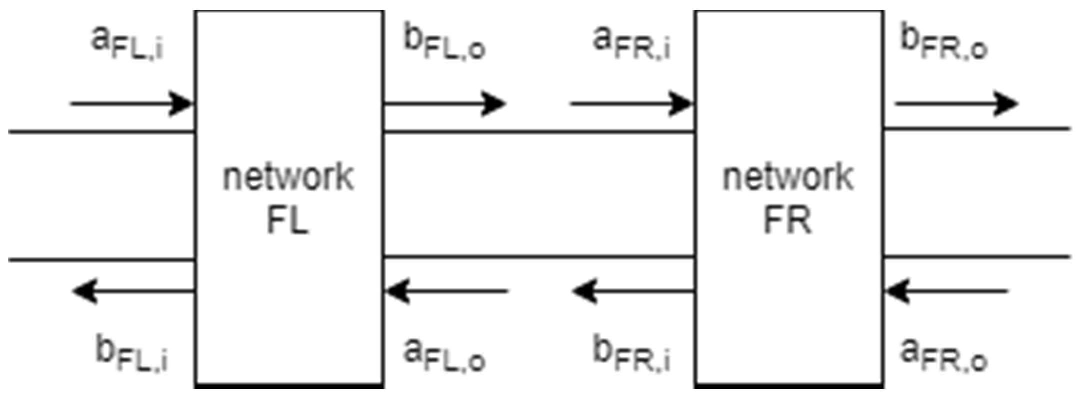
Figure 1. Cascade of two 2-port S-parameter networks: “FL” stands for left feature network and “FR” stands for right feature network.
Electronics 10 01275 g001
Figure 2. System of three 2-port S-parameter networks to be cascaded.
Electronics 10 01275 g002
Figure 3. (a) Overview of the full de-embedding setup, (b) details of the FL and FR fixtures, (c) complete fixtures from the original multiport model.
Electronics 10 01275 g003aElectronics 10 01275 g003b
Figure 4. Comparison of the S-parameters obtained by: 1. the standalone original device under test (DUT) considered as reference (continuous line “Orig. DUT”), 2. the classic standard two-steps S-to-T and T-to-S parameter conversion (dashed line “S-T conv. De-embed”), 3. the single-step procedure (circles “Single-Step De-embed.”) and 4.by the numerical iterative solution (dash-dot line “Numerical calc.”). (a) S21, (b) S11, (c) S22.
Electronics 10 01275 g004aElectronics 10 01275 g004b
Table 1. Maximum absolute error for the de-embedding methods considered.
MethodS11S22S21
Classic standard three-step (S-T conv. De-embedding)6.15 × 10⁻⁹ + j × 1.08 × 10−81.09 × 10−9 + j × 3.9 × 10−92.04 × 10−8 + j × 3.8 × 10⁻⁹
Proposed
single step (Single-Step De-embed.)
6.15 × 10⁻⁹ + j × 1.08 × 10−81.09 × 10−9 + j × 3.9 × 10−92.04 × 10−8 + j × 3.8 × 10⁻⁹
Numerical solution (Numerical calc.)1.08 × 10⁻⁵ + j × 1.4 × 10−50.03 + j × 0.0251.30 × 10−4 + j × 7.33 × 10⁻⁴
Table 2. Root mean squared difference for the considered de-embedding methods.
MethodS11S22S21
Classic standard three-step (S-T conv. De-embedding)9.26 × 10⁻¹⁸ 7.76 × 10⁻¹⁸ 2.09 × 10⁻¹⁷
Proposed single step (Single-Step De-embed.) 9.26 × 10⁻¹⁸ 7.76 × 10⁻¹⁸ 2.09 × 10⁻¹⁷
Numerical solution (Numerical calc.)3.29 × 10⁻¹¹ 2.20 × 10⁻⁴ 6.51 × 10⁻⁸
Publisher’s Note: MDPI stays neutral with regard to jurisdictional claims in published maps and institutional affiliations.