Article

Compact and Low-Profile On-Chip Antenna Using Underside Electromagnetic Coupling Mechanism for Terahertz Front-End Transceivers

by
Mohammad Alibakhshikenari
1,*,
Bal S. Virdee
2,
Ayman A. Althuwayb
3,*,
Dion Mariyanayagam
2 and
Ernesto Limiti
1
1
Electronic Engineering Department, University of Rome “Tor Vergata”, Via del Politecnico 1, 00133 Rome, Italy
2
Center for Communications Technology & Mathematics, School of Computing & Digital Media, London Metropolitan University, London N7 8DB, UK
3
Department of Electrical Engineering, Jouf University, Sakaka 72388, Saudi Arabia
*
Authors to whom correspondence should be addressed.
Electronics 2021, 10(11), 1264; https://doi.org/10.3390/electronics10111264
Submission received: 17 April 2021 / Revised: 16 May 2021 / Accepted: 24 May 2021 / Published: 25 May 2021
(This article belongs to the Special Issue Advances in System-on-Chip Design)

Abstract

:
The results presented in this paper show that by employing a combination of metasurface and substrate integrated waveguide (SIW) technologies, we can realize a compact and low-profile antenna that overcomes the drawbacks of narrow-bandwidth and low-radiation properties encountered by terahertz antennas on-chip (AoC). In addition, an effective RF cross-shaped feed structure is used to excite the antenna from its underside by coupling, electromagnetically, RF energy through the multi-layered antenna structure. The feed mechanism facilitates integration with the integrated circuits. The proposed antenna is constructed from five stacked layers, comprising metal–silicon–metal–silicon–metal. The dimensions of the AoC are 1 × 1 × 0.265 mm3. The AoC is shown to have an impedance match, radiation gain and efficiency of ≤ −15 dB, 8.5 dBi and 67.5%, respectively, over a frequency range of 0.20–0.22 THz. The results show that the proposed AoC design is viable for terahertz front-end applications.

1. Introduction

The interest in terahertz (THz) bands (0.1–10 THz) is steadily growing, as this band enables several important applications, such as biomedical imaging, ultrafast wireless communication, remote non-destructive inspection of packaged goods, security screening, and medical drug applications [1,2]. The current terahertz systems are of low power and low sensitivity. This necessitates the development of terahertz antennas for on-chip applications [3]. Several complementary metal–oxide–semiconductor (CMOS) on-chip antennas have been studied and manufactured to meet the demand of terahertz radio, on-chip, front-end circuit systems [4]. However, most of the terahertz on-chip antennas have problems of low radiation efficiency and narrow bandwidths, which are caused by increased losses from substrate and conductors and the very thin thickness of the substrate between the antenna and ground-plane [5,6]. Standard rectangular CMOS on-chip patch antennas have shown fractional bandwidths and radiation efficiencies of less than 10% [7,8].
In this paper, metasurface and substrate integrated waveguide (SIW) technologies are used to overcome the restrictive bandwidth, radiation gain and efficiency limitations for small antennas [9,10,11]. A combination of these two technologies is used to design a compact, low-profile, high-performance terahertz integrated-circuit antenna for on-chip applications. The mechanism used to excite the proposed antenna on-chip uses a cross-shaped feeding structure that is located on the underside of the multi-layered antenna through electromagnetic radio frequency (RF) coupling. The benefits derived from the proposed approach are the reduced substrate loss, suppressed surface-waves, and the enlargement of the antenna’s effective aperture. As the results below reveal, the consequence of this is the widening of the impedance bandwidth and the increased radiation performance with no compromise in the total form factor of the antenna.

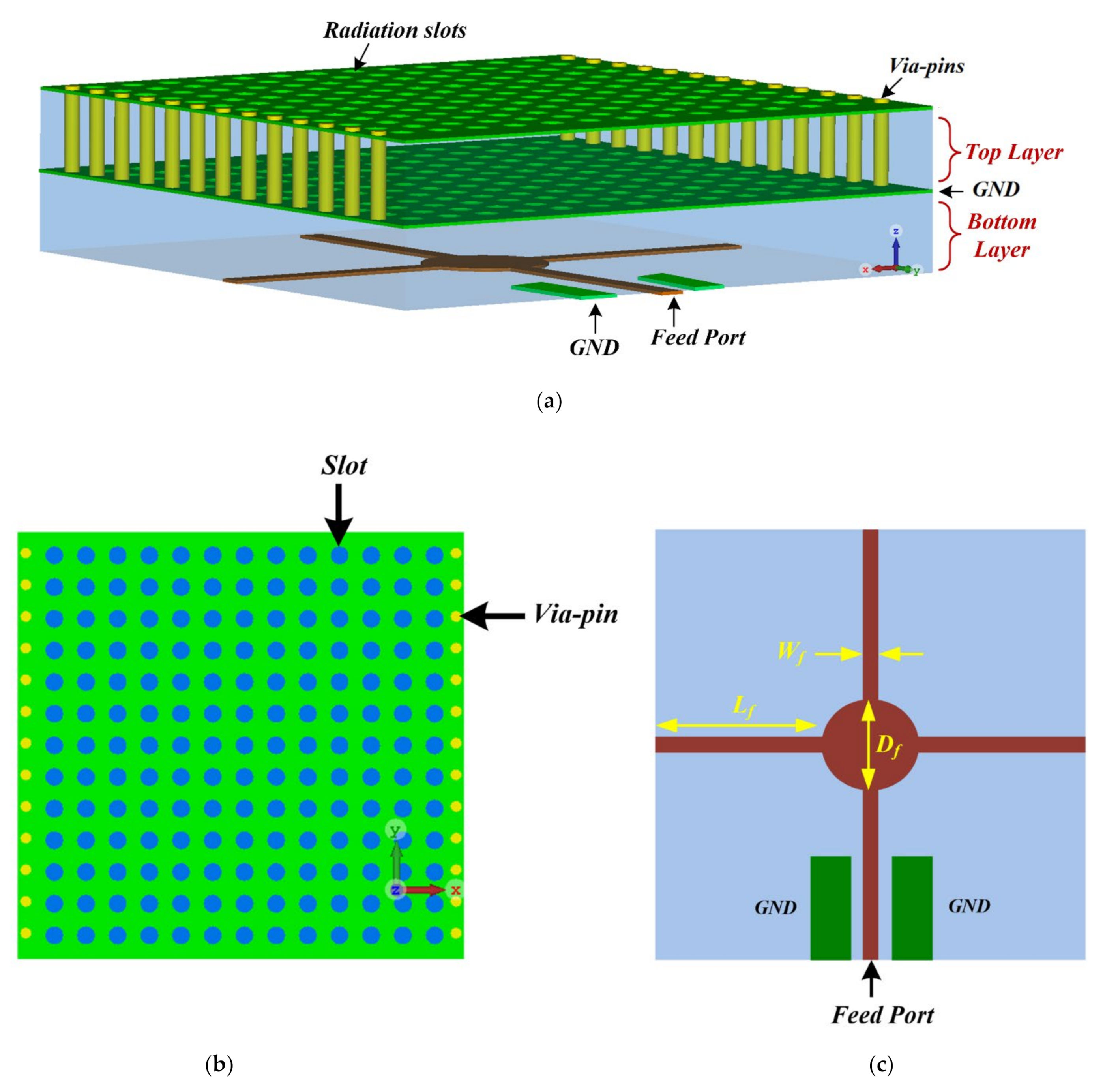
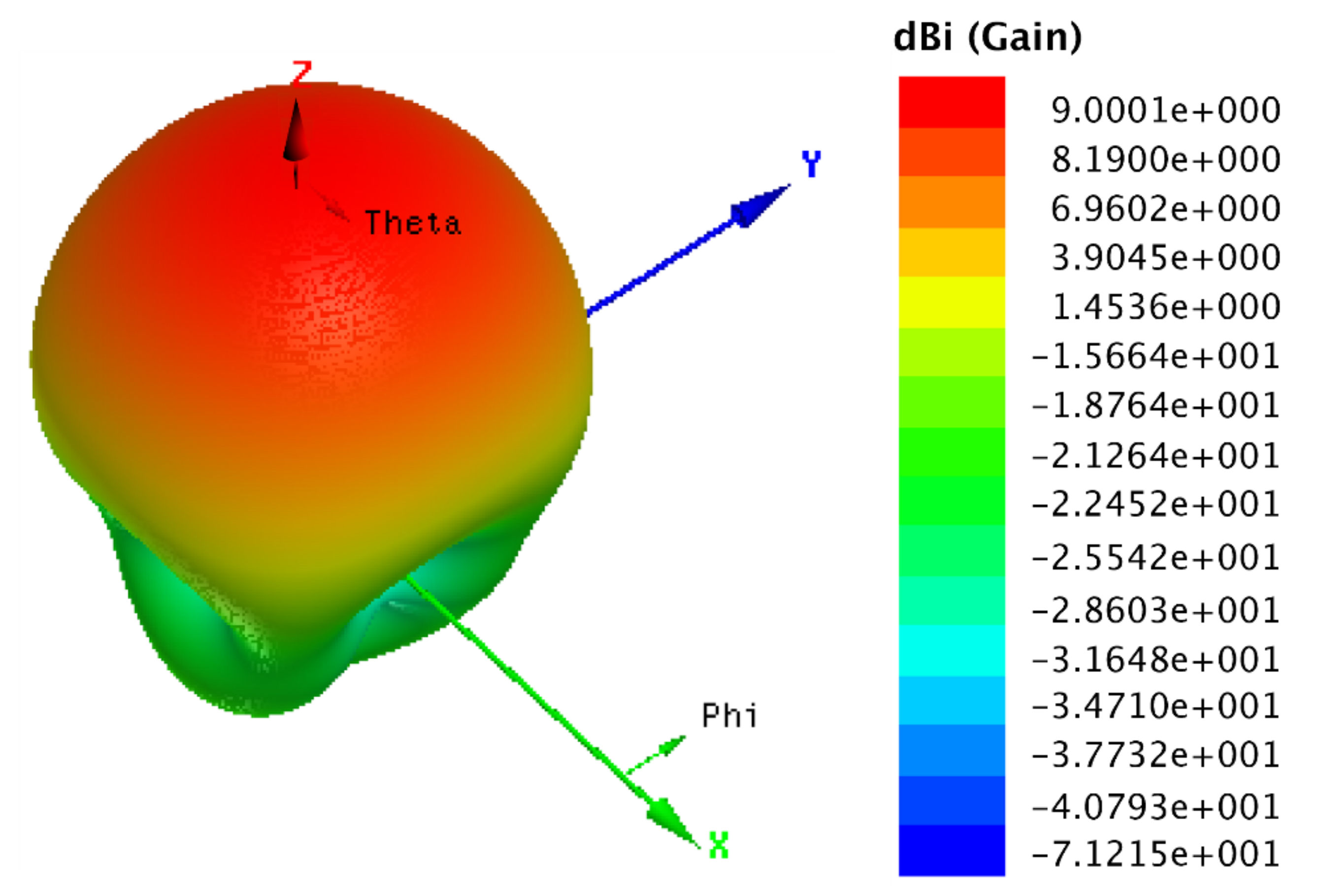
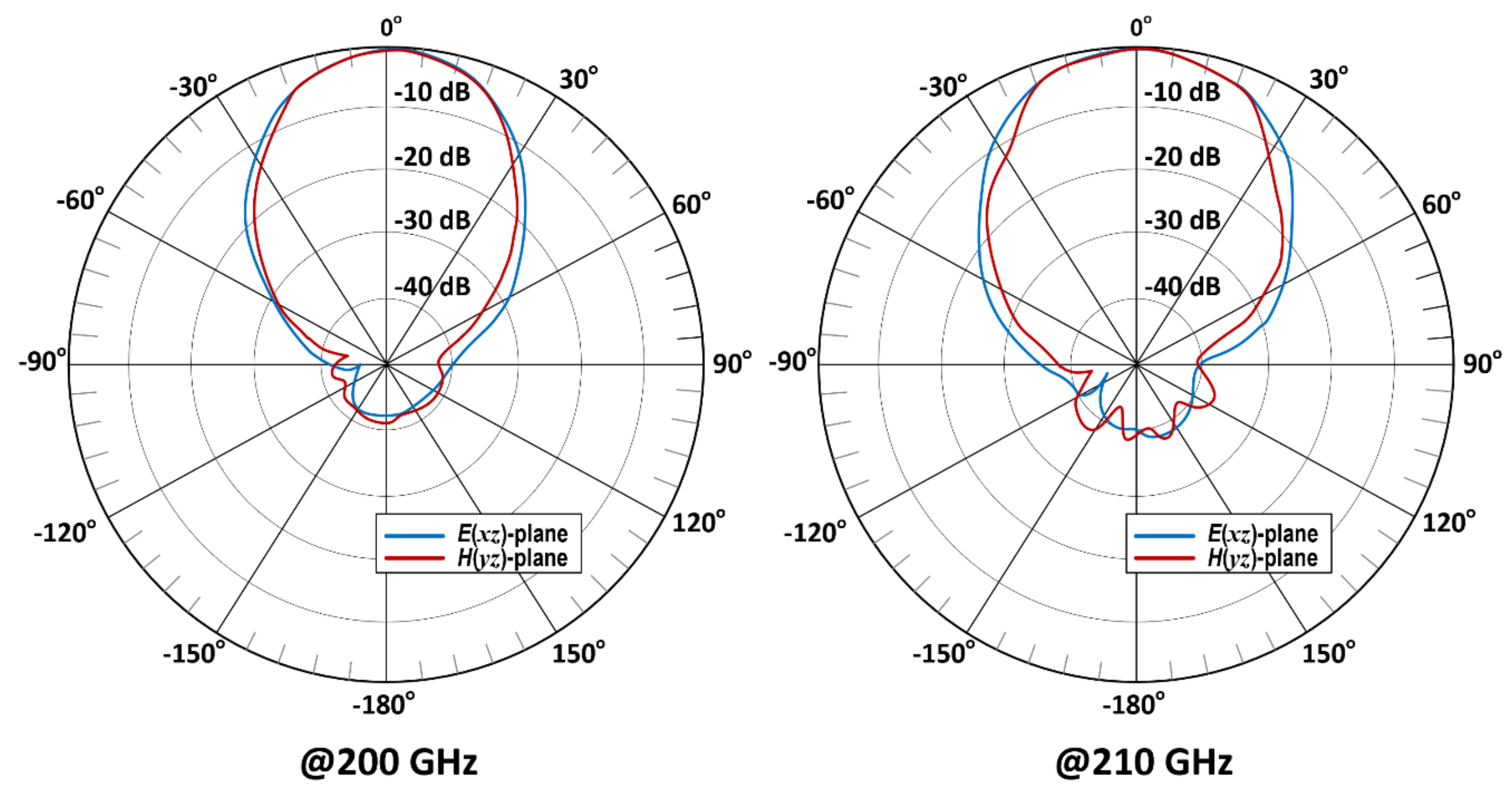
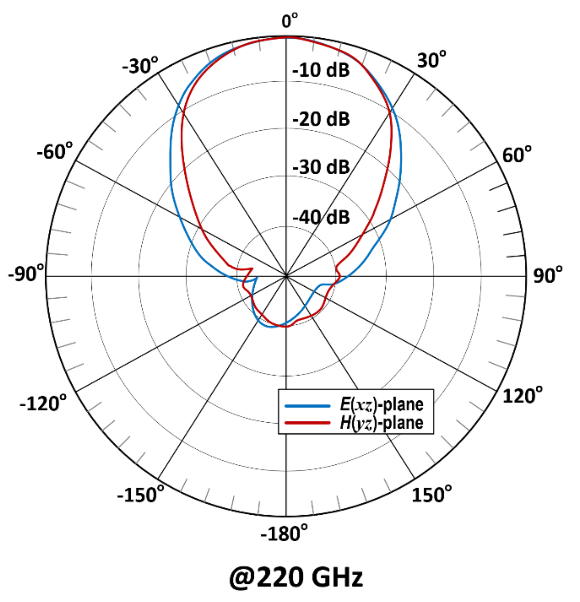
2. High Performance Antenna On-Chip

The realization of a high-performance antenna in terms of frequency range, radiation gain and efficiency for on-chip implementation is a highly challenging endeavor, due to the small effective aperture area of the chip as well as the adverse effects of the surface waves and substrate loss. To overcome these issues, we employed metasurface and substrate integrated waveguide (SIW) technologies.
The proposed compact on-chip antenna is fabricated on a stack of five layers comprising metal—silicon—metal—silicon—metal. The top silicon layer is sandwiched with two very thin metal layers made of aluminum. The parallel metal layers sandwiching the silicon layer are perforated with a periodic arrangement of circular slot holes, and the two outer edges of the metal layers are connected to each other with metal pins through the silicon layer to create the SIW structure, as shown in Figure 1a,b. The cavity created by the SIW structure only supports the transverse electric (TE) mode because of the gaps between the metallic pins on the side walls of the cavity. The thickness of the silicon substrate is carefully chosen so that the dominant cavity mode is outside the frequency range of interest. The diameter and spacing of the circular slot holes on the extremely thin metal layers are chosen such that the circular slot holes are of subwavelength diameter and the periodicity of the slots is small in comparison to the wavelength of operation [12]. Configuring the metal layers in this fashion causes them to manipulate the electromagnetic (EM) waves that impinge upon them in such a way that is characteristic of metasurfaces, which are a two-dimensional counterpart of metamaterials. This structure has an effect of enhancing the effective aperture area of the antenna [13]. The proposed SIW structure reduces substrate loss, radiation leakage and the adverse effects of surface wave propagation, the consequence of which is enhancement in the radiation gain and efficiency of the antenna. In addition, the slots also improve the impedance match and bandwidth of the antenna.
The mechanism used to excite the antenna is electromagnetically coupling RF energy from a cross-shaped microstrip-line structure that is fabricated on the bottom side of the second silicon layer, as shown in Figure 1. One of the ports is used as the feed port and the other three ports of the cross-shaped feed structure are open-circuited ends. At the junction of the cross is a circular patch whose diameter facilitates the matching of the feedline to the antenna. The antenna is excited through a coplanar waveguide (CPW) feedline, which is realized by being located at the loss proximity to the feedline at the ground-plane. This structure confines the electromagnetic energy within the dielectric and enables the feedline to be implemented on a single plane. Electromagnetic energy from the CPW port excites the feeding structure’s three tentacles that couple the RF energy through the two silicon layers and the circulars slots. The ground-plane (GND) metal layers have a thickness of 5 μm. The silicon layers of 125 μm thickness have a dielectric constant of 11.9 and loss tangent of Tan( δ ) = 0.00025. The dimensions of the structural parameters of the AoC are given in Table 1.
Two different 3D full-wave electromagnetic computational techniques, i.e., CST-Microwave Studio and HFSS Designer, are used to validate the proposed antenna’s characteristics, namely, the reflection coefficient (S11), radiation gain and efficiency response. CST is based upon the Finite Integration Technique (FIT) and HFSS is based on the Finite Element Method (FEM). The reflection coefficient, radiation gain and efficiency performance across the antenna’s operating frequency range are shown in Figure 2. There is excellent correlation between the two computational techniques. It is evident from Figure 2a that the proposed antenna operates from 0.2 THz to 0.22 THz for S11 better than −15 dB. The antenna’s radiation gain and efficiency across its operating frequency vary between 8.15 dBi and 9 dBi, and 60% and 72.5%. The average radiation gain and efficiency are 8.7 dBi and 67.50%, respectively. The optimum gain and efficiency are noted at 210 GHz.
The three-dimensional radiation pattern of the on-chip antenna at 210 GHz in Figure 3 shows a simulated gain of +9 dBi with boresight pointed toward the z-axis. Co-polarization radiation patterns at the E(xz)-plane and H(yz)-plane at the lower, middle, and top end of its operating frequency are plotted in Figure 4. Stable broadside radiation and almost symmetrical EH-plane patterns are also observed over a wide frequency band. The front-to-back ratio is about 10 dB mainly due to the residual leakage. No side-lobes are observed from the antenna.
The above results confirm that the proposed multilayer antenna structure, implemented with metasurface and SIW technologies, can yield a compact and low-profile antenna for on-chip application that operates across a wide frequency range from 200 GHz to 220 GHz for a reflection coefficient better than −15 dB. Moreover, it is capable of a radiation gain of 9 dBi and an efficiency of 72.5%. The antenna structure is suitable for applications in terahertz, RF, on-chip, front-end wireless systems.

3. Conclusions

The feasibility of a novel antenna on-chip design is presented for wideband, high-gain and high-efficiency for terahertz integrated-circuit applications. The antenna design combines metasurface and substrate integrated waveguide technologies implemented on a multi-layered silicon substrate. The coplanar waveguide port of a cross-shaped microstrip line was used the excite the antenna from the underside of the bottom silicon substrate. The antenna’s radiation pattern was stable over its operating frequency range. This was achieved by coupling EM energy through the silicon layers to the circular slots implemented on the metallized silicon layers. The results confirm that the proposed antenna is compatible for fully integrated terahertz transceiver systems.

Author Contributions

Conceptualization, M.A., B.S.V., and E.L.; methodology, M.A., B.S.V., and E.L.; software, M.A., B.S.V., and D.M.; validation, M.A., B.S.V., A.A.A., D.M., and E.L.; formal analysis, M.A., and B.S.V.; investigation, M.A., B.S.V., and E.L.; resources, M.A., B.S.V., A.A.A., D.M., and E.L.; data curation, M.A., B.S.V., A.A.A., D.M., and E.L.; writing—original draft preparation, M.A.; writing—review and editing, M.A., B.S.V., A.A.A., D.M., and E.L.; visualization, M.A., and B.S.V.; supervision, M.A., and E.L.; project administration, M.A., and E.L.; funding acquisition, M.A., and E.L. All authors have read and agreed to the published version of the manuscript.

Funding

This research received no external funding.

Data Availability Statement

Data are contained within the article.

Conflicts of Interest

The authors declare no conflict of interest.

References

  1. Woolard, D.L.; Brown, R.; Pepper, M.; Kemp, M. Terahertz Frequency Sensing and Imaging: A Time of Reckoning Future Applications? Proc. IEEE 2005, 93, 1722–1743. [Google Scholar] [CrossRef]
  2. Pawar, A.Y.; Sonawane, D.D.; Erande, K.B.; Derle, D.V. Terahertz Technology and its Applications. Drug Inven. Today 2013, 5, 157–163. [Google Scholar] [CrossRef]
  3. Alibakhshikenari, M.; Virdee, B.S.; Khalily, M.; See, C.H.; Abd-Alhameed, R.; Falcone, F.; Denidni, T.A.; Limiti, E. High-Gain On-Chip Antenna Design on Silicon Layer With Aperture Excitation for Terahertz Applications. IEEE Antennas Wirel. Propag. Lett. 2020, 19, 1576–1580. [Google Scholar] [CrossRef]
  4. Sankaran, S.; Mao, C.; Seok, E.; Shim, D.; Cao, C.; Han, R.; Arenas, D.J.; Tanner, D.B.; Hill, S.; Hung, C.-M.; et al. Towards Terahertz Operation of CMOS. In Proceedings of the 2009 IEEE International Solid-State Circuits Conference-Digest of Technical Papers, San Francisco, CA, USA, 8–12 February 2009; pp. 202–203. [Google Scholar] [CrossRef]
  5. Cavallo, D.; Syed, W.H.; Neto, A. Efficiency and Bandwidth Enhancement of on-Chip Antennas by Using Connected Arrays and Artificial Dielectrics. In Proceedings of the 2016 41st International Conference on Infrared, Millimeter, and Terahertz waves (IRMMW-THz), Copenhagen, Denmark, 25–30 September 2016; pp. 1–2. [Google Scholar]
  6. Syed, W.H.; Fiorentino, G.; Cavallo, D.; Spirito, M.; Sarro, P.M.; Neto, A. Design, Fabrication, and Measurements of a 0.3 THz On-Chip Double Slot Antenna Enhanced by Artificial Dielectrics. IEEE Trans. Terahertz Sci. Technol. 2015, 5, 288–298. [Google Scholar] [CrossRef] [Green Version]
  7. Zhu, H.; Li, N.; Zeng, J.; Li, X.; Ai, B. A Novel 0.22-THz On-Chip Antenna Based AMCs. In Proceedings of the Asia-Pacific Microwave Conference, Sendai, Japan, 4–7 November 2014; pp. 366–368. [Google Scholar]
  8. Abdellatif, A.S.; Taeb, A.; Safavi-Naeini, S.; Schmalz, K. A Terahertz High-Efficiency On-Chip Antenna. In Proceedings of the 2014 IEEE Antennas and Propagation Society International Symposium (APSURSI), Memphis, TN, USA, 6–11 July 2014; pp. 1485–1486. [Google Scholar]
  9. Caloz, C.; Itoh, T. Electromagnetic Metamaterials: Transmission Line Theory and Microwave Applications; John Wiley & Sons, Inc.: New York, NY, USA, 2005; Volume 7, pp. 316–322. [Google Scholar] [CrossRef]
  10. Alibakhshikenari, M.; Virdee, B.S.; Ali, A.; Limiti, E. Extended Aperture Miniature Antenna Based on CRLH Metamaterials for Wireless Communication Systems Operating Over UHF to C-Band. Radio Sci. 2018, 53, 154–165. [Google Scholar] [CrossRef]
  11. Wu, K.; Cheng, Y.J.; Djerafi, T.; Hong, W. Substrate-Integrated Millimeter-Wave and Terahertz Antenna Technology. Proc. IEEE 2012, 100, 2219–2232. [Google Scholar] [CrossRef]
  12. Bozzi, M.; Pasian, M.; Perregrini, L.; Wu, K. On the Losses in Substrate-Integrated Waveguides and Cavities. Int. J. Microw. Wirel. Technol. 2009, 1, 395–401. [Google Scholar] [CrossRef]
  13. Jiang, Z.H.; Yun, S.; Lin, L.; Bossard, J.A.; Werner, D.H.; Mayer, T.S. Tailoring Dispersion for Broadband Low-loss Optical Metamaterials Using Deep-Subwavelength INCLUSIONS. Sci. Rep. 2013, 3, 1571. [Google Scholar] [CrossRef] [PubMed] [Green Version]
Figure 1. Geometric structure of the proposed AoC, implemented using metasurface and SIW technologies, (a) isometric view, (b) top metallic layer embedded with circular slot holes of sub-wavelength diameter and periodicity of the slots is smaller than the wavelength of operation, and (c) cross-shaped microstrip feedline structure implemented on the bottom-side of the lower silicon layer.
Electronics 10 01264 g001
Figure 2. Performance of the proposed AoC, (a) reflection-coefficient response, (b) radiation gain, and (c) radiation efficiency.
Electronics 10 01264 g002
Figure 3. The full three-dimensional radiation pattern of the on-chip antenna at 210 GHz.
Electronics 10 01264 g003
Figure 4. Simulated normalized radiation patterns of the proposed antenna at 200 GHz, 210 GHz, and 220 GHz in the xz- and yz-planes.
Electronics 10 01264 g004aElectronics 10 01264 g004b
Table 1. Geometrical design parameters.
ParameterDimensions
Thickness of silicon layers125 μm
Thickness of metal layers5 μm
Radius of slots20 μm
Gap between slots30 μm
Radius of via-pins12 μm
Height of via-pins135 μm
Gap between via-pins46 μm
Lf (see Figure 1)400 μm
Wf (see Figure 1)40 μm
Df (see Figure 1)200 μm
Surface area of AoC1000 × 1000 μm2
GND plane1000 × 1000 μm2
Publisher’s Note: MDPI stays neutral with regard to jurisdictional claims in published maps and institutional affiliations.

