1. Introduction
With the advent of Internet of Things (IoT) and wearable devices, connectivity and portability became core features for numerous embedded systems. Connectivity and system integration led to an explosion of the amount and complexity of functionalities that can be potentially supported, while portability often implies stringent constraints on power consumption, which need to be tackled since the first design steps to be met. Cyber-Physical Systems (CPS) era brought sensors and actuators within embedded and IoT systems in many different markets [
1], making them interactive with physical processes, environment, and humans, as well as reactive to their status/requirements [
2,
3]. Application Specific Integrated Circuits (ASICs) constitute one of the best options to tackle CPS performance constraints as area reduction, energy consumption minimization and speed maximization, but they generally lack in flexibility/adaptivity. Latest Field Programmable Gate Arrays (FPGAs) constitute a valuable alternative, embedding on the same chip flexible general purpose processing resources and efficient programmable logic. In any case, to meet the adaptivity needs of CPS, heterogeneous and flexible platforms where different kinds of processing elements, interconnects and memories can be exploited, became the preferred choice. However, from the designer perspective, heterogeneity does not come for free and multiple complementary competencies, ranging from hardware (HW) to software (SW) skills, are required to develop such systems.
On the application side there is also an increasing demand for execution efficiency. In video technology, resolution is constantly augmenting, for example, going from 4 K to 8 K format required 24.9 M more pixels (+300%), with common rates that go from 60 to 120 fps. The information growth and the stringent time constraints are translated into an increased complexity for video algorithms, for example, video codecs. Dedicated HW has become an appealing solution for such issues, where computation intensive applications lie under strict constraints. Thus, heterogeneous adaptive CPS often involve dedicated HW accelerators to efficiently tackle onerous and constrained tasks within applications. However, designing dedicated HW requires advanced digital design skills and longer development time with respect to the standard SW design flow, and it is even harder when reconfigurable computing is adopted within HW accelerators to achieve the adaptivity required by CPS.
Design automation has been conceived to simplify the design process when complexity and time are raised up, and High Level Synthesis (HLS) has become very popular in the last years—starting from a high level description of a functionality, HLS tools derive HW specifications, usually in terms of Hardware Description Language (HDL), ready to be processed by digital design tools for FPGA or ASIC design. The increased need for HW acceleration pushed the main FPGA and ASIC stakeholders to put huge effort in HLS tools [
4,
5], and the number of HLS solutions has growth in the last years also on the academical side [
6]. It is true though that HLS-derived solutions are not as good as manually optimized ones, neither in terms of timing performance nor in terms of consumed power. Often, designers are required to make code refactoring or to use specific pragmas in the input high level specification to get better solutions. Moreover, the adopted HLS tool has a great impact on the resulting HW specification in terms of adopted resources and performance, and it is strictly related to the targeted technology.
HLS usually does not provide any support for adaptivity/reconfiguration, nor for system-level low power management. Power consumption is managed at physical level, through the power management features provided by digital design tools. Moreover, in HW design it is not possible to know the optimal trade-off among different metrics a priori, and design iterations in the implementation steps might be necessary to meet the desired performance. System-level power management would help when a low power accelerator is needed, but it requires to be aware of the effectiveness of the applied technique, which in turn may depend on the adopted HLS tool. Some works tried to address the power management at system-level [
7,
8,
9] and in some cases they also tackled design automation for HW acceleration and adaptivity [
10,
11]. However, to the best of our knowledge, there are no works in the literature that study the mutual impact of the chosen HLS and the adopted the power management strategy.
Within this context, focusing on reconfigurable accelerators, the main contributions of this work are:
the analysis of the effectiveness of several HLS tools in the implementation of low-power HW accelerators for heterogeneous and adaptive systems;
the exploration of the mutual impact between different HLS strategies and a simple low power technique, clock gating, applied at various levels. As far as we know, this is the first time that a similar study, investigating HLS and clock gating peculiarities together, is proposed in literature. Traditionally, clock gating is either applied at region or actor level, as it will be better explained in
Section 3. Nevertheless, to cover a wider range of possibilities, in this paper we also propose a novel
multi level clock gating approach for dataflow based reconfigurable HW accelerators;
the assessment and comparison of the different clock gating solutions, including the new one, on a video coding use case while adopting multiple HLS tools and target technologies;
the derivation of hints and guidelines for an optimal application of clock gating and for its future integration on an automatic design flow for dataflow based HW accelerators.
The main objective of this work is to understand the relationships between HLS tools and CG application at different levels considering dataflow based reconfigurable accelerators. In particular, on one hand peculiarities related to HLS tools are considered, like implemented models of computation, hardware communication protocols, latency of the generated hardware, while on the other CG related aspects, such as level of application and target technology, are considered. The conducted study is intended as a preliminary work under the view of a future design automation for the addressed devices, so that hints and guidelines for driving the process in order to achieve an optimal behavior under different metrics, namely resource occupancy, maximum frequency and power, are investigated and highlighted.
From the conducted study and experiments it will be clear as the new proposed multi level clock gating technique ensures optimal performance in ASIC independently from the adopted HLS tool. However, when resources are strictly constrained, other techniques, such as region level clock gating, could be better solutions since they trade resources at the price of higher power consumption. In FPGA actor level clock gating is instead outperforming the other techniques for most of the cases. Nevertheless, in this case the adopted HLS tool is important, since results may change depending on the generated code complexity and on the activity percentage of the design. Generally speaking, HLS and its user driven aspects (pragmas and code shaping) determine differences in implementation which bias clock gating effectiveness and, thus, should be taken into consideration when applying the same clock gating techniques.
The rest of the paper is organised as follows—
Section 2 describes the background of the proposed work.
Section 3 shows the details of the conducted study including the new proposed clock gating solution.
Section 4 extensively analyses the obtained experimental results, deriving hints and guidelines for future design automation.
Section 5 concludes the work with some final remarks.
3. Materials & Methods
The current literature does not offer a completely automated support for reconfigurable HW accelerators where optimal power management is provided on the basis of the adopted HLS tool. In this work we explore, on the one hand, the correlation between the adopted HLS tool and CG effectiveness. At this purpose, in
Section 3.1 different HLS tools are considered and analyzed, trying to highlight all the peculiarities which may play a role when CG is applied on top of them, such as target technology, latency, implemented communication protocol or the adopted model of computation. While, on the other hand, the mutual impact between HLS tools and different CG strategies (
Section 3.2), applied at different levels. In this case, the peculiarities of the HLS tools are reflected to the specific considered CG strategy, discussing if they have an impact or not. Being the
region level and the
actor level already know, we will introduce also a novel
multi level solution, to cover all the possible ranges of application.
3.1. HLS Tools
The HLS tools may differ for several aspects. A first difference lays on the adopted input specifications, which can be mainly classified as imperative or functional languages/ frameworks. Imperative specifications describe functionalities as a sequence of instructions, such as in a C program. They are very common, especially in commercial HLS, since imperative languages are extremely diffused, thus can reach a wider public. Functional specifications refer to modular descriptions where modules describe operations, while connections define the data communication between modules. Functional HLS, like dataflow based ones, already revealed to be more suitable for generating reconfigurable HW [
13]. Nevertheless, imperative HLS tools can still be exploited within functional based designs to selectively generate the HDL corresponding to the actors, while leaving to the functional specification the connections description. On top of that, imperative HLS tools make user control points (i.e., preferences for HLS flow or pragmas to be inserted within the original input specification) available to the developer, to optimize the generated HW. Being compliant also with imperative HLS tools, we target functional, dataflow based designs.
Another difference among HLS tools is related to the target technology: there are target-agnostic and vendor-specific HLS tools. These latter are usually capable of generating efficient HDL specifications for the targets they are conceived for. From the implementation point of view, a different internal description of the actors is translated in different communication protocols and latency. At last, the generated HDL could be easily readable or not. When it is, designers could attempt further optimizations after the HLS generation process.
According to their features, different HLS tools may have a different impact on the effectiveness of CG. To provide a representative exploration we consider three different HLS tools:
CAPH [
6], an academic HLS tool based on dataflow specifications, to be provided in CAPH language, and capable of generating generic target-agnostic HDL code;
STRATUS [
5], the Cadence official HLS engine based on classical imperative C code specifications, generating target-agnostic HDL code for dataflow actors;
VIVADO [
4], or more precisely Vivado HLS, Xilinx official HLS engine based on classical imperative C specifications, generating vendor-specific HDL code for dataflow actors to be implemented over Xilinx FPGAs boards.
By considering three different ways of generating actors (see
Table 1 for a summary of the HLS tools features) we ensure a robust assessment of the studied approach. All the actors generated with the considered HLS tools implement FIFO based communication protocols, which differ for the kind of signals and handshake implemented on the interface between actors and FIFOs. In particular, CAPH and VIVADO provide classical
empty/full signals on the FIFO side and
write/read signals on the actor side. STRATUS, instead, adopts a protocol based on
valid and
busy signals present either on actors and FIFOs, depending on the interface (input or output), and performing data transmission when
valid is asserted and
busy is not asserted. Dealing with actor latency, CAPH and VIVADO generate actors that perform actions in one single clock cycle, while STRATUS actors may require more than one clock cycle (a
busy signal is used to indicate that the processing is still ongoing).
3.2. Clock Gating Application Levels
CG acts on the dynamic power performing a logic
AND between an enable signal and the clock signal in order to shut it off when the driven logic is unused. To avoid glitches on the resulting gated clock, the enable signal goes throughout a clock falling edge sensitive
FF before driving the AND gate [
32]. So that, one single two-input AND gate and one FF are sufficient to implement CG. Here comes the simplicity of such kind of low power technique.
Dataflow based HW accelerators have a data driven execution, meaning that action firing depends on tokens availability in the incoming FIFOs and on free slots availability, to store the produced data, in the outgoing FIFOs. According to this, it is straightforward to define the first possible level for the application of CG: the
actor level one. CG at actor level can be performed by considering as enable signals the complementary of
empty and
full status flags of the incoming and outgoing FIFOs. This is the kind of approach already used in the works of Bezati et al. [
11] and Fanni et al. [
27]. A higher level CG can be applied at the
region level.
LRs can be defined as sets of processing elements in a digital design that are always active/inactive at the same time, and could be enabled/disabled to optimize power consumption. Such kind of approach has been already successfully adopted in the work of Palumbo et al. [
10]. In this paper we consider both
actor level and
region level CG to investigate the impact of the specific adopted HLS on it. Moreover, a novel CG technique, named below as
multi level, is presented.
One of the objectives of the proposed work is gathering hints and guidelines for a perspective design automation of CG within the considered context. In References [
10,
11] design automation for
actor level and
region level CG has already proven to be feasible. Thus, once a strategy for obtaining optimal CG efficiency according to the chosen HLS tool and target technology will be defined, the design automation of its application is straightforward. This is true also considering
multi level CG, since it is basically a combination of
actor level and
region level CG, so that its support in design automation, which will be performed in future works, should be feasible as well.
3.2.1. Actor Level
Actor level CG operates over actors, switching them off to avoid useless refresh of internal registers. More precisely, when an actor is inactive, then also the read logic of the incoming FIFOs and the write logic of the outgoing FIFOs are inactive. For this exploration we consider designs in which the FIFOs, based on the ones presented in Reference [
11], are implemented as asynchronous FIFOs, with disjointed clock ports for the read and write logic, so that they can be gated together with the corresponding actor.
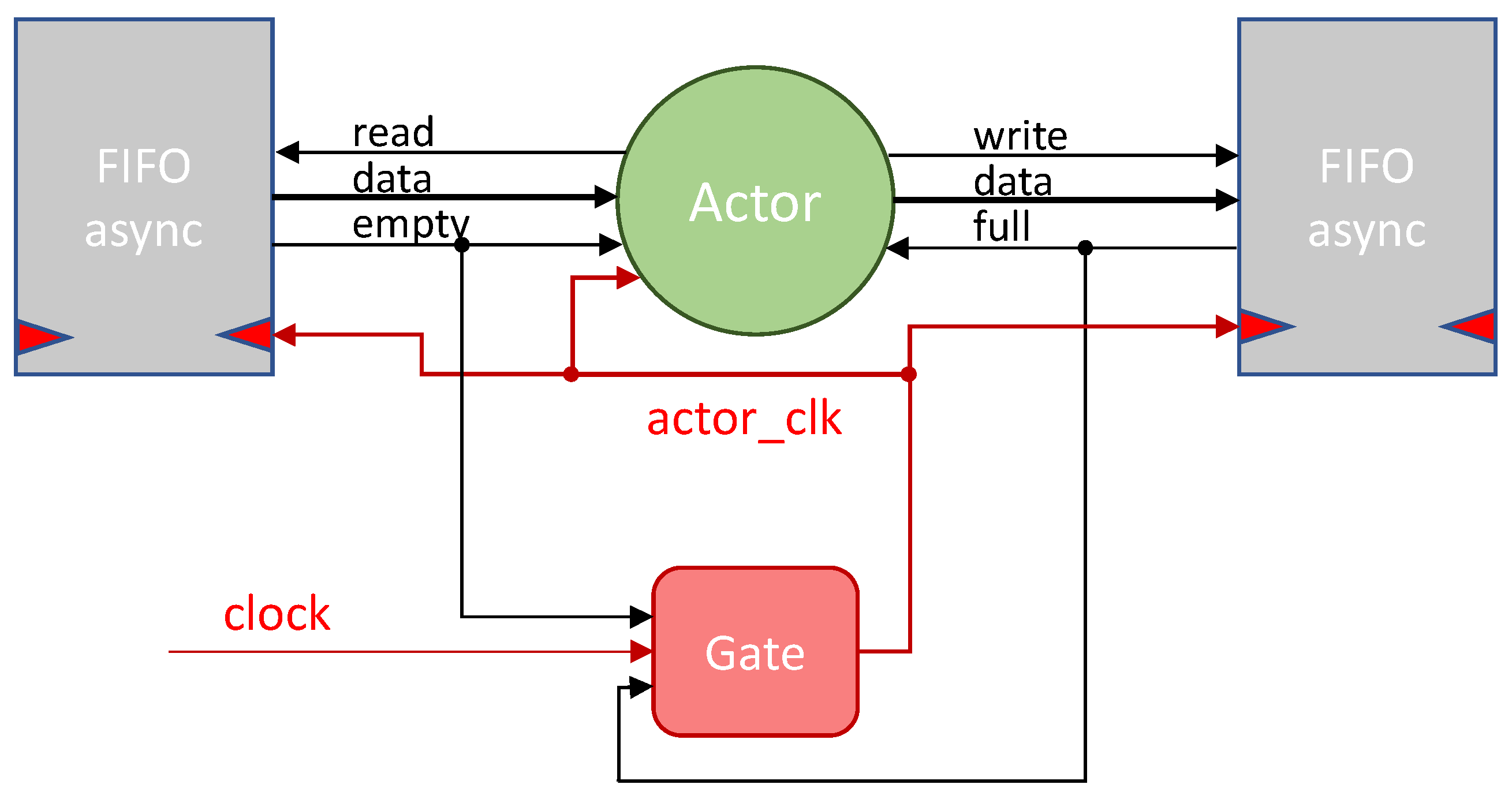
Figure 2 shows the main scheme of the
actor level CG implemented in this work. The clock signal actor_clk, driving the actor, the incoming FIFOs and the outgoing FIFOs, is provided by the gate module that derives it by performing the logic
AND between the main clock source, clock, and an enable obtained as the
NOR between
empty and
full flags of the involved FIFO buffers. The adopted HLS tool may impact on different aspects of such CG application level:
Communication Protocol: the communication protocol among actors of the chosen HLS can play a role in the way gating is performed. If the actor and/or the FIFOs need more than one clock cycle to check the firing conditions, read data and finalize transmission, such delay has to be taken into consideration when gating the logic. In this case, a state machine is necessary inside the gate module to properly manage the gating process [
11]. For instance, if a communication protocol takes different clock cycles to read a token (check the conditions, read the data, and acknowledge the reception), then the gate module has to wait for the completion of the reading operation before shutting down the clock.
Dataflow MoC: the adopted dataflow MoC impacts on which FIFO flags have to be considered to provide the enable signal for the gate module. In deterministic MoCs, the token production and consumption rates are constant, and it is simple to derive the clock enable, thus the logic necessary to implement it can be smaller. For instance, if an actor always reads one token from port A and then one from port B, the gating logic can be built taking into consideration subsequently and disjointedly the empty signals of port A and port B.
Actions Latency: the time required by actors to fire actions and process data impacts on the gate module. A busy condition due to ongoing actions has to be generated and considered to avoid switching off an actor while computing. For instance, an actor taking 5 clock cycles to produce one output token after consuming one input token should be kept on for all the 5 cycles, even if the input FIFO goes empty after the token consumption.
In this work we adopt communication protocols that always require one single clock cycle for data transfer, so that the state machine inside the gate module of Bezati et al. [
11] is no longer necessary and simple gates performing a logic
AND between the clock signal and a registered enable are employed. The adopted MoC is Cyclo Static DataFlow [
33], meaning that the consumption/production rates of the actors on the surrounding FIFOs change cyclically among a finite set of possibilities. However, for the sake of simplicity, all the FIFOs are always taken into consideration and the corresponding
empty and
full signals are used to derive the CG enable. In particular, all
empty and
full signals related to each actor are put in
AND together and then negated to derive the clock enable. So that, as long as data/free space are present in at least one FIFO around the actor, the clock will be kept valid and the computation will not be corrupted. In some of the considered designs, the enable also depends on actions latency, since certain actors take more than one clock cycle to process data and to finalize firings. In such cases,
empty and
full signals are combined with a
busy signal, coming from the actor, to generate the CG enable. In particular,
busy signal, when present, is put in
OR with the negated
AND of
empty and
full signals of FIFOs surrounding the actor.
3.2.2. Region Level
LRs, as already introduced, contain sets of processing elements that can be enabled/ disabled together. These
LRs are highly common in coarse-grained reconfigurable systems, in which different functionalities share common resources. The kind of adopted reconfiguration is virtual, since functionalities are enabled by multiplexing resources over time. For this peculiarity, they can be implemented on different technologies (FPGA and ASIC), thus allowing for a certain degree of flexibility, limited by the functionalities specified at design time.
LRs not involved in the current computation can be switched off. To guarantee a high presence of
LRs and a wider case study with respect to the one of Reference [
28], in which reconfiguration was not tackled, we select coarse-grained reconfigurable systems, leveraging also on the availability of the open source MDC tool that automatically implements such kind of systems, and that is already capable of identifying the
LRs and implementing CG on top of them [
10].
Each
LR is driven by a gated clock whose enable is derived directly by the current configuration of the system.
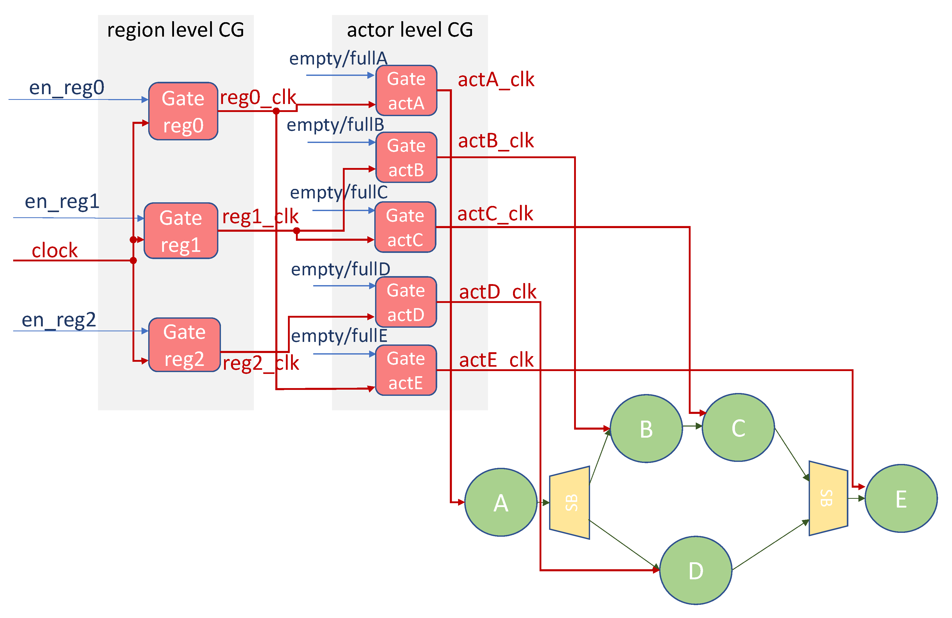
Figure 3 depicts an example of
region level CG implementation for dataflow based reconfigurable accelerators. The system is composed by five actors,
A,
B,
C,
D and
E, and two different functionalities can be performed (
Func1 and
Func2): actors
A,
B,
C and
E are used by
Func1, while actors
A,
D and
E by
Func2. According to this composition of the system, three
LRs can be identified:
reg0 shared between the two functionalities (actors
A and
E);
reg1 involving actors adopted only by
Func1 (
B and
C); and
reg2 involving actors adopted only by
Func2 (
D). As a result, three gates are necessary to apply
region level CG in such a system. The enable signals of such gates are derived by a
Clock Configurator module according to the currently executed functionality: for
Func1,
reg0 and
reg1 are enabled, while for
Func2,
reg0 and
reg2 are enabled. Please, notice that
reg0 is always on when one of the two functionalities is enabled. However, it can be gated when the accelerator is in idle, for example, when a full SW part of the application is executed.
Differently from actor level CG, region level CG is not influenced by the chosen HLS, nor by the adopted dataflow MoC. Indeed, in this case CG is applied at a higher level of abstraction, far from implementation details such as the FIFOs signals or actors communication protocol.
3.2.3. Multi Level
Region level CG can save the power consumed by those LRs not involved in the current computation, which means that if a LR is necessary for the selected operation, its actors are active for the whole computation regardless of their actual activity. On the other hand, actor level CG, taking into consideration the individual activity condition of each actor (empty, full and, optionally, busy signals), is capable of saving power in any part of the system and in each moment of the execution. In fact, if a certain actor is involved in the current computation, but it has not received tokens yet, it can be switched off to save power. Actor level CG has a higher resource overhead since it requires one different gate for each actor within the system, while region level CG requires one gate per LR, which are normally less than the number of actors, plus the Clock Configurator that is a quite simple module. A combination of these two CG levels could potentially bring additional benefits by switching off the LRs not involved in the current functionality and, at the same time, by switching on/off the individual actors of the active regions according to their actual activity.
Starting from the
region level CG example of
Figure 3,
Figure 4 illustrates the combination of
actor level and
region level CG. A hierarchy of gate modules is needed. The outer clock gates derive a clock for each identified
LR (
reg0_clk, reg1_clk, reg2_clk). These clock signals, instead of directly driving the logic within their respective
LRs, drive the second level of clock gates connected to each actor and related FIFOs. In this way, when
Func2 is enabled,
reg1 is disabled since the beginning of the execution through
region level CG, while the rest of the actors is enabled/disabled according to their activity, by means of
actor level CG. The same occurs for
reg2 and the rest of the actors when
Func1 is enabled.
Being multi level CG a combination of actor and region level CG, it inherits their dependencies from the selected HLS and dataflow MoC. In particular, the same HLS aspects impacting on actor level CG are valid here too. Moreover, of course, it will consume more resources than the single strategies applied in a standalone manner.
4. Results
For the proposed analysis we adopted a video processing application (
Section 4.1). As already said, the aim is to investigate the mutual impact between different HLS tools and the CG technique applied at different levels, and then derive some guidelines for perspective automation of power management in coarse-grained reconfigurable accelerators, enabling the selection of the optimal CG approach given the selected target and HLS flow. Besides three different HLS tools (CAPH, STRATUS and VIVADO), we also explored two different technologies: ASIC (
Section 4.2) and FPGA (
Section 4.3).
Besides a comparison between the different HLS tools and CG application levels, in the FPGA case a deep dive into HLS user knobs, specifically pragmas and code refactoring, their consequences on generated code and, in turn, their impact on the CG effectiveness is also proposed. Please note that CG in such technologies implies extremely different aspects: while in ASIC it is possible to build from scratch the entire clock tree, in FPGA the clock tree is already there, and it is recommended to modify it only through dedicated resources, that is, the clock buffers (BUFG) for Xilinx devices. Moreover, as explained in
Section 2.2, modern FPGAs have already available resources with clock enables for safe and efficient CG application, avoiding common issues related to clock slack and synchronization. These CG compliant resources are considered in the proposed study (more details are provided in
Section 4.3).
For an easier reading of the main findings related to the conducted analysis, a summary with hints for future design automation, highlighted through a square containing the text, is provided for each subsection.
4.1. Designs Under Test
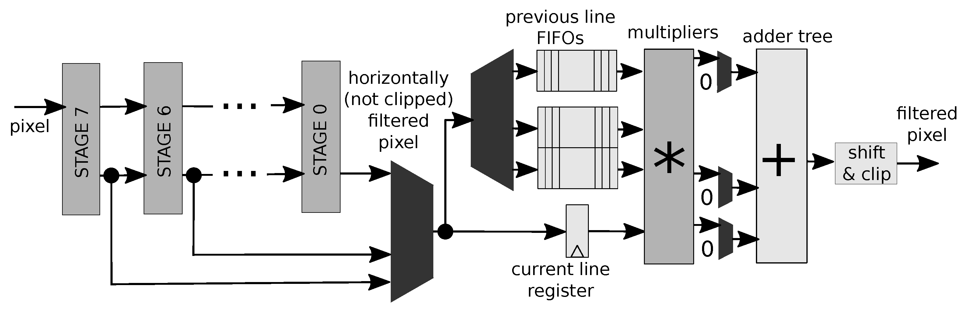
As test case for the proposed analysis we adopted a video coding application: an interpolation filter for luma color components adopted in the motion estimation/compensation of the High Efficiency Video Coding (HEVC) standard [
34]. The effect of the filtering is basically a two dimensional FIR filter performing a shift of the input image block by fractional pixel positions. A HW accelerator capable of adapting the interpolation quality and energy consumption has been developed. Dataflow models of the interpolator with 8, 5 and 3 tap FIR filters have been combined together using the MDC tool, so that the generated reconfigurable accelerator can change its configuration among the different configurations (8, 5 and 3 tap), executing them one at a time (see
Figure 5). HDL code corresponding to the dataflow actors has been derived through the three considered HLS tools. Trade-offs are there: processing is more precise but more energy consuming with 8 taps, and less precise but less energy consuming with 3 taps, while 5 taps provides intermediate behavior for both metrics. Such a reconfigurable HW interpolator constitutes an example of an adaptable component for heterogeneous CPS.
Table 2 depicts the composition of the dataflow models corresponding to the available interpolator configurations. Five different
LRs have been identified, partitioning the set of 61 involved actors. As expected, the most precise and power hungry configuration, 8 tap, is also the one employing more actors, 51. On the contrary, the less precise and consuming configuration, 3 tap, is using only roughly one third of the available actors, 21.
Four designs have been developed for each adopted HLS engine:
In summary, 16 designs will be considered in the following: 4 per each HLS, 3 HLS tools overall, one of them adopted twice (STRATUS and STRATUSr) to provide a focus on some implementation details which can play an important role within the presented analysis (see
Section 4.4).
Table 3 provides a complete overview of the designs under test, showing also how they cover the two considered target technologies (only CAPH and STRATUS designs target also ASIC). The table adopts the just defined labels (
base is the design without CG,
actor with actor level CG,
region with region level CG, and
multi with multi level CG) to concisely present the designs developed for each considered HLS and target technology.
CG at different levels has been applied by hand on the reconigurable HW interpolators provided by MDC and involving actors HW specifications generated by the different HLS tools. In all the considered cases, the manual nature work does not causes subjective biases on the obtained design, meaning that having done it automatically would have led to the same result. This is because, once the CG logic and the CG application levels are defined, they can be implemented in a unique way for the considered context.
For the assessment phase, and in particular dealing with power numbers which consider real switching activity gathered during post-synthesis simulations, the same testbench has been adopted for all the designs. The interpolator elaborates a 16 × 16 monochromatic image surrounded by a zero padding frame to allow the computation of border pixels, since the output image has the same size of the input one. Data are provided in the input FIFOs one per clock-cycle (according to FIFOs full condition), so that each design elaborates inputs at its maximum achievable rate.
4.2. Assessment on ASIC
Assessment on ASIC has been performed on a CMOS 45 nm technology library (Cadence 45 nm generic standard cell database, GSCLIB045), for the CAPH and STRATUS derived designs, while VIVADO is not usable in the ASIC flow. Since memories in the design are limited and, as it will be clearer in
Section 4.4, concurrent read and write accesses are required in some actors, specific memory library and compilers have not been adopted but all the sequential logic is implemented through FFs. Resource occupancy, frequency and power estimation data (see
Table 4) refer to post-synthesis designs and have been obtained with the Cadence Genus Synthesis Solution. For accurate power estimation, real post-synthesis switching activity has been retrieved using Cadence Xcelium Parallel Logic Simulation. Resource and power numbers are gathered at 100 MHz for all the designs to provide a fair comparison with FPGA ones, whose maximum frequency is slightly above 100 MHz. Applying different CG strategies resulted in a negligible resource overhead, always below 0.25%. Please note that in the
region case it is more than one order of magnitude lower than the others. When STRATUS is used to generate the actors, due to additional
busy signals and logic in the
actor level gates (see
Section 3.2.1),
actor and
multi CG require more resources.
Table 4 shows also that CG never impacts on the maximum achievable frequency for both the considered HLS, independently from the entity of such frequency. Indeed, STRATUS designs are twice faster than CAPH ones: shorter critical paths are there since STRATUS actors require several clock cycles to fire, thus involving less combinatorial logic within sequential one. In particular, STRATUS designs have the combinatorial datapath broken by registers, resulting in slower execution (it requires more than one clock cycle) but at a higher maximum achievable frequency.
Power data reveal the benefits of applying CG strategies on such kind of systems. As expected, since every CG strategy is acting on the number of unused resources, the more the number of taps are, the larger the used resources and power consumption are. Comparing the different CG strategies, we can notice how region CG designs are almost always the less efficient ones, since they are capable of acting only on the inactive LRs of the system. Actor and multi CG designs, instead, are capable of saving power also in the active LRs, where they act basically in the same way. The multi CG approach seems to be the best choice for both CAPH and STRATUS. This means that the application of the region CG on top of the actor one makes it possible to save more power due to the clock tree, and it is mostly due to the inactive LRs where multi and actor behave differently. In general, the bigger the inactive LR is, the higher the power saving is with both actor and multi solutions. Actor CG approach acts on the inactive actors and related FIFOs, thus shutting down entire inactive LRs since all the FIFOs are empty there. While multi CG gates the whole region clock tree, which is wider for bigger LRs.
We can notice as the benefits of multi CG approach with respect to the actor one depend on the considered HLS engine. While for STRATUS the benefit is almost tangible for all the configurations, this is not in the CAPH case. This fact comes from the higher complexity of the gate modules adopted for STRATUS designs (that have to consider the busy signal too) with respect to the ones used for CAPH ones. In fact, shutting off also the gate modules results in a larger saving when they are more complex.
Summary and Hints
When an ASIC technology is targeted, multi level CG is always the most effective choice to optimize power, even if the resulting additional saving with respect to a simpler actor level CG strategy is not always appreciable. Nevertheless, going from actor to multi, the resource overhead increment is extremely low and there is no frequency drop, thus multi level CG should always be applied. Considering a future automation of the optimal CG application, the multi shall be to be considered in all cases, but when the area occupancy is critical, meaning that by looking at the base design the area is already close to the constraint. In this last case a trade-off which leads to sub-optimal power efficiency but with smaller area overhead (actor or region CG) could be preferable.
Considering different HLS engines and, in turn, different HDL descriptions for actors and gates, simpler combinatorial actors, such as in CAPH case, lead to smaller savings when actor level CG (actor or multi designs) is adopted. On the contrary, region level CG is more effective with such kind of HLS tools. Moreover, region level CG can reach similar savings than other solutions but employing less resources when most of the design is often inactive (as in the 3 tap case), if a CAPH-like HLS is adopted. If a STRATUS-like HLS is used, instead, actor or multi solutions are always significantly better options than the simple region one, regardless the configurations usage frequency.
4.3. Assessment on FPGA
FPGA assessment has been conducted on all the three considered HLS tools (CAPH, STRATUS and VIVADO) targeting an Artix-7 XC7A50TCSG324 28 nm device. Resource occupancy data have been gathered by means of Vivado and refer to post-synthesis (out of context) designs. Frequency data are instead obtained through complete implementation of the designs with Vivado, using different timing constraints. Power data have been extracted with Vivado Power Estimator, using real post-synthesis switching activity (Vivado Simulator has been used for simulations). Resource and power numbers are gathered at 100 MHz, which is a bit lower than the minimum among the maximum achievable frequencies of the FPGA designs.
As we said, in the latest FPGA devices, FFs and BRAMs provide dedicated clock enable inputs for performing CG. To exploit such features, it is necessary to let synthesis tools know which are the gated clocks, so that they can use the gating logic to drive the clock enable inputs, instead of acting directly on the clock in a less efficient manner. In the proposed exploration, this option has been enabled according to the process described by the considered FPGA and synthesis tool vendor in Reference [
35]. According to this process, by properly setting the
gated_clock_conversion Vivado synthesis parameter and by accordingly introduce
gated_clock attributes for the clocks to be gated in the HDL descriptions, Vivado identifies the gating logic to drive the FFs and BRAMs clock enables.
In
Table 5 it is observable the same trend of ASIC assessment in terms of resources utilization. CG requires a very low overhead, up to 6.2% of LUTs and up to 1.3% of FFs overall. DSPs and BRAMs, employed only for complex arithmetical operations and big data storing, are not affected by CG. It is possible to notice that STRATUS designs experience a larger resource overhead due to CG than other HLS tools. While in the ASIC case this behaviour was simply caused by the more complex gating logic that involves also the actors state in the
actor and
multi designs, in FPGA this is not the only reason. In fact, the larger overhead is appreciable in the
region designs too, where the CG strategy does not consider the actor state. The premise we made on how the synthesizer uses the clock enable ports can explain this different behaviour. Since every CG strategy acts on the clock enable port, which is also used in
base designs for automatic CG synthesis by Vivado, the combination of automatic and explicit CG leads to a different resource overhead with respect to the expected one.
In terms of frequency, CG can cause a drop due to additional delays coming from the overhead logic. This drop is always present in the multi designs and it is maximum using STRATUS HLS (−6.3% with respect to base), since it is the one with the biggest LUT overhead overall. The actor designs do not present any additional frequency drop since the added gating logic is driven by signals close to the gated sequential resources. Differently, in region and multi designs, the gating modules consider top level signals, far from the gated resources.
Power results, reported in
Table 6, show as the effectiveness of the considered CG strategies varies depending on the interpolator configuration and on the used HLS tool. Indeed, CAPH and STRATUS designs are not able to save any power for the 8 tap configuration, that has the highest amount of active resources. In such cases, the
region CG strategy is the one behaving worst, since the saving depends on the inactive logic (minimal in this case). On the contrary, VIVADO CG designs save up to 6.3% of power with respect to the
base one, for all the considered CG strategies. Considering the 5 and 3 tap configurations, CG designs are always capable of saving power. As in ASIC, the larger the inactive region is, the higher the saving is. This means that going from 84% to 54% active actors (see
Table 2), that means going from 16% to 46% inactive actors, all the CG strategies for all HLS cases start saving power. For all the considered HLS engines the lowest consuming design is a CG solution running the 3 tap configuration, whose range of saving goes from the 8% in CAPH to the 18.3% in STRATUS. Differently from ASIC results, the
multi solution is not the best option, apart from the STRATUS case in 3 tap configuration. In all the other cases,
actor CG achieves always the highest power saving. Such trend is due to the flattening of the CG logic hierarchy operated by the synthesizer to optimize the resulting logic used to drive clock enable ports. Thus, the
multi advantages, due to clock tree and inactivity of actors within regions, are often nullified by the synthesizer optimization. To better understand these results, both
base resource utilization and resource overhead due to CG have to be considered. In particular, STRATUS designs behave worse than the others in the 8 tap configuration, but better in the 3 tap configuration. The negative behavior in the 8 tap case can be attributed to the larger resource overhead with respect to other HLS engines, which prevent any power saving when most of the logic is on. On the other hand, as will be extensively discussed in
Section 4.4, most of the STRATUS power saving is obtained from BRAMs, which are not used in the other designs. Since this saving happened to be significant, it leads to a greater effectiveness of CG strategies in the 3 tap case, but is nullified in the 8 tap, when all the BRAMs are active (since they are used by
line_buffer actors, which are all active in this case).
Summary and Hints
In summary, actor level CG is almost always the best choice on FPGA, guaranteeing the best power saving with limited resource overhead and without frequency drop. However, when actors take more than one clock cycle to fire and additional busy signals are necessary, multi CG could outperform actor CG in terms of power if most of the design is inactive (such as for STRATUS in 3 tap configuration). More studies on these aspects are necessary to model and automate CG application, due to the additional impact of the FPGA synthesizer choices/options.
4.4. Impact of Implementation Choices: The STRATUS HLS Case
STRATUS designs seem to behave differently from the others in the FPGA assessment. As described in
Section 4.1, such HLS generates actors employing more than one clock cycle to fire and demanding a
busy signal to drive the clock. In addition to the larger number of clock-cycles to fire, STRATUS presents another relevant difference with respect to the other HLS engines: by default, it considers only single port RAMs in the HLS process. In the evaluated test case, the
line_buffer actor, that is in charge of storing one row of the horizontally interpolated image, writes a new element in its memory while reading the old one during each action-firing. Concurrent write/read accesses imply that if a RAM resource is adopted, then it should be double port. To overcome this issue, two possibilities have been explored:
Both the possibilities require to act on the HLS with pragmas or code refactoring. Data reported in
Table 5 and
Table 6 labeled as STRATUS refer to the second possibility, the one employing two single port RAM resources. For this reason the STRATUS trend in FPGA is different from the other HLS tools, and a deeper investigation of implementation aspects was needed to analyze the impact of the possible choices.
The following discussion compares the solution which uses two single-port RAMs (STRATUS in
Table 5) with the register bank solution (STRATUSr in
Table 7). In the STRATUSr
base design, LUTs and FFs are almost doubled with respect to the STRATUS ones, meaning that implementation moved from coarser-grain storing (BRAMs) and computing (DSPs) resources to finer-grain ones (FFs and LUTs respectively). It is interesting what happens in the CG STRATUSr solutions: the amount of LUTs explodes, so that the resulting designs exceed the available resources on the target device. When registers are gated, each of them is driven by a separated clock enable coming from dedicated gating logic. When BRAMs, instead of FFs, are employed for implementing the memories (STRATUS design), less LUTs are necessary to gate them, since more than one register and more than one bit is fitting in one single BRAM resource, thus requiring less gating logic. Due to the target device fitting issue, the frequency analysis for the STRATUSr designs has been carried out only in the
base case. The achievable frequency is 111.1 MHz, as in the STRATUS
base design.
The huge amount of LUTs necessary to gate the equally large number of sequential resources is reflected directly on power performance as shown in
Table 8. From the STRATUSr 8, 5 and 3 tap total entries, none of the proposed CG solutions is capable of providing power saving. Rather, every CG solution is consuming more power than the
base one, from +30% of the
actor CG design in the 3 tap configuration, to the +54% of the
multi one in the 8 tap configuration. Looking more in detail at the different contributions of the dynamic power consumption in the STRATUSr designs, it is possible to observe a saving in terms of clock related power, that is the contribution due to clock buffers and sequential logic. Thus, the desired saving is present also in STRATUSr, since clock related power is always decreased in CG designs with respect to the
base one. However, such saving is not visible on the total dynamic power amount due to power overheads in other contributions. A power overhead is present in signal and logic terms, which are related to signal propagation and logic resources within slices (including LUTs) respectively. Signal and logic terms for
actor,
region and
multi CG designs have a considerable increase from a minimum of +39% for signal in the 3 tap configuration to a maximum of +153% for logic in the 8 tap one. Please, notice that, even if it is not visible in
Table 8, the increase is due to the higher number of signal and resources, not to an increase on the power consumption of each of them. In summary, the observed behavior is directly connected to the specific implementation of CG STRATUSr designs, where a big number of FFs requires a big number of gating signals and logic. Taking a look at STRATUS 8, 5 and 3 tap entries of
Table 8 it is possible to appreciate how, also in this case, CG designs have an overhead in terms of signal and logic contributions, since additional logic and signals are present with respect to the
base design. However, in the STRATUS case, the overheads are lower (up to +7% in the logic 8 tap case) and do not overcome the benefits obtained by other contributions. These latter are clock, as for STRATUSr designs, and BRAM, not present before.
Summary and Hints
From the provided focus on implementation aspects it is clear how the behaviour of the applied CG strategy is strongly related to the specific implementation. This latter not only depends on the adopted HLS engine, despite all the examples in this section are focused on the usage of the STRATUS HLS engine, but also on code refactoring and pragmas employed for code generation. Both functional aspects, that is, number of clock-cycles required for actor firings, and non-functional aspects, that is, target technology resources employed to realize actors, are important. To model these aspects and take them into account when applying CG automatically, back annotated synthesis data could be considered, that is, the target resources employed to realize actors.
5. Conclusions
Embedded electronics has entered in the era of cyber physical systems and internet of things. Adaptivity and heterogeneity turned out to be useful to cope with such an extremely challenging context. At the same time, power optimization and design effort minimization are crucial, and should be both met, to speed-up time to market without compromising performance. Dataflow based reconfigurable HW accelerators constitute a suitable solution for the addressed scenario, delivering heterogeneity and adaptivity, while being supported by tools to relieve designers from low level details definition.
In this work we investigated the mutual impact between different clock gating strategies and some high level synthesis tools that can be adopted to derive the HW specifications, under the perspective of future automation of the optimal clock gating for the chosen target and design environment. The investigated clock gating strategies involve literature solutions and a new proposed one, each of them acting at a different level, while the considered high level synthesis engines come from both industry and academia, and evaluated targets are both ASIC and FPGA. The final aim of the conducted study is to understand if useful hints for future design automation, optimally applying CG on the addressed devices, can be retrieved by the proposed preliminary work. Results show that, for ASIC target technologies the new proposed multi level clock gating seems to be always the best choice, but when resources are critical. In case of FPGAs, instead, actor level clock gating seems to be preferable, but for complex actors and when most of the design is inactive. However, as deeply discussed, high level synthesis knobs produce implementation differences, which have an impact on the clock gating effectiveness, thus the back annotation of implementation details could be useful to pursue optimal automated system generation.
Future studies will be directed towards a deeper characterization of the implemented actors and the definition of models to automate the process and support designers in the definition of the proper clock gating strategy to be selected, according to the addressed targeted technology, the chosen high level synthesis flow and the application configurations usage frequency. In particular, the plan is to implement an initial automated strategy from the outcomes of the proposed work, to test it on a wider set of applications, and to validate and refine the same strategy in order to achieve the optimal performance.


