1. Introduction
The development of electron microscopy methods required for the comprehensive study and control of the phase composition and surface structure of composite materials is necessary to carry out quantitative analysis of small-scale areas with nanometer spatial resolution. The solution to this problem lies in the field of the development of various methods and techniques for increasing the brightness of an electron gun by using cathodes of various geometries (for example, sharp-tip field emitter arrays (FEA) [
1]), as well as creating new materials [
2,
3]. As an example, one could mention the gradual replacement of wire-type hot emitters based on thoriated tungsten filaments with cathodes made of lanthanum hexaboride and similar materials [
4].
One of the most effective electron microscopy methods is the electron energy loss spectroscopy technique (EELS), which is based on the possibility of analyzing and using different behaviors of elastically and inelastically scattered electrons. Elastically scattered electrons are not taken into account in the EELS method, while electrons experiencing inelastic losses practically do not change the direction of their trajectory. The collection of electrons occurs from a local area, comparable in size with the diameter of the electron beam. With the development of field emitters, it became possible to conduct a quantitative analysis in nanoregions, rather than microregions, which, however, required solving a number of problems, including the necessity to enhance the stability of incident electrons in terms of energy, to implement energy discriminators with a narrow window, and to increase the electron flux density. As a result, only those electrons are selected that have undergone one-time collisions (i.e., one-time characteristic energy losses), while the receiver detects the electrons that were not deflected and separates them according to their energy.
It should be noted that in the case of modern field emission cathodes, the current density values can reach 108 A/m2, by several orders of magnitude exceeding the achievable values for classical Richardson–Schottky field enhanced thermionic emitters.
Thus, the problem of increasing the current density of electron sources is relevant, both from a purely scientific perspective and the practical point of view, as a technique that can be successfully utilized to solve technical problems of electron microscopy methods for the analysis of grain boundaries in nanophase materials, which is extremely important for metal and mineral sciences [
4,
5].
Modern studies [
6,
7,
8] have indicated that the use of the low-macroscopic field emission phenomenon as a means to reduce the threshold electric field strength magnitudes applied to the cathode makes it possible to obtain comparable current density values in much lower fields (in the range between 1 V·μm
−1 and 40 V·μm
−1) than those for which cold field emission (5 V·nm
−1) is usually observed [
9], thus leading to a further increase in the efficiency of this class of devices. For example, the authors of [
8] investigated the field emission properties of cathode prototypes based on amorphous nanoporous carbon (NPC). It is assumed that for this structure, the existence of a low-macroscopic field emission phenomenon is due to the presence of conducting nanoparticles, which contribute to the concentration of electric field at their internal boundaries. The authors note that such an effect is preferable from the practical implementation standpoint for a wide range of devices, since, unlike the already mentioned sharp-tip field emitters, the field amplification area is protected from external impacts, such as, for example, ion bombardment. The NPC structures in consideration demonstrated emission properties at threshold field strength values of 2 V/μm to 3 V/μm.
We chose porous silicon (PS) as a base material for our prototype low-macroscopic field emission cathode due to the prospect of creating a regular PS matrix characterized by a highly specific surface area [
10,
11,
12], which facilitates its further functionalization [
10] as well as the introduction of nanoscale coatings [
12,
13], quantum objects [
14], and thin layers [
15] for a wide range of distinctive fields of application, including optoelectronics [
16], targeted drug delivery [
10], and gas sensing [
10]. In addition, earlier studies demonstrated successfully synthesized porous silicon of various spatial configurations and morphology, as well as composite nanostructures based on it [
17,
18].
It should be noted that while treating the experimental data, many authors have used simplified interpretations of various subjects related to the emission of electrons from composite and amorphous structures. Insufficient attention has been paid towards quantum-size phenomena (for example, the formation of two-electron (2e) and two-hole (2h) centers with negative correlation energy). This fact is all the more important since the analysis of the solutions to optimization problems of modern instrumentation and material processing [
19,
20], namely the design, manufacture, implementation of devices and prototypes [
21], diagnostics (including the development of local micro- and nanodiagnostic systems) [
22], as well as control and infocommunication systems [
23], indicates the existence of uncertainty and only the relative possibility of its reduction based on reliable quantitative optimizing information in the form of physical models [
24,
25,
26] describing the relationship between the recorded signals and the interaction processes of various physical fields with matter.
Despite a fairly large number of existing attempts to theoretically describe the process of low-macroscopic field emission, including Latham’s model of low-threshold emission [
27], Forbes’s model of internal field amplification [
28], as well as the model of field emission from semiconductor structures with negative electron affinity [
29], the mechanisms of this phenomenon still remain unclear.
Thus, the potential of low-macroscopic field cathodes, characterized by a high electron flux density, as well as a simultaneous decrease in the threshold field strength values for creating electron sources has been widely discussed in literature [
30,
31,
32].
During our studies, both field emission properties and the structure of novel cathode prototypes predicated on porous silicon functionalized with silver-doped fullerene (C60)—based structures were studied. A low-macroscopic field emission effect model based on the formation of two-electron (2e) centers with negative correlation energy was proposed.
2. Materials and Methods
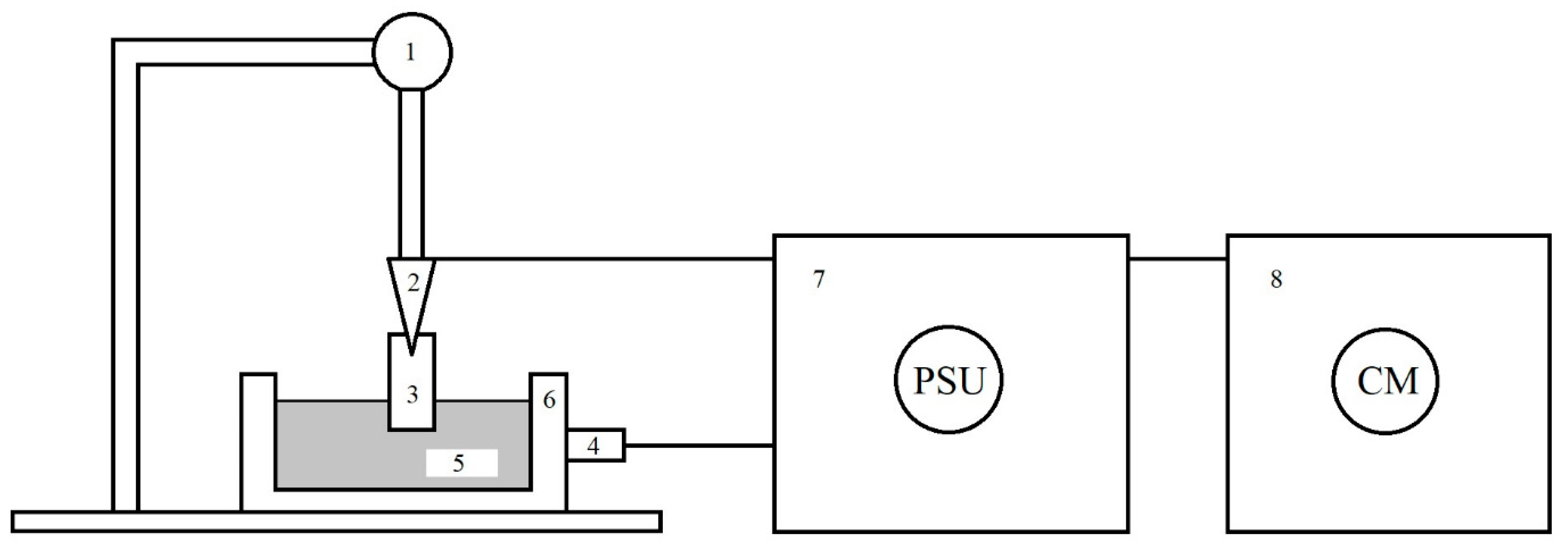
To obtain a matrix of porous silicon, we used the method of electrochemical anodic etching. Monocrystalline p-type silicon with (100) crystallographic orientation of KDB-12 brand was used as a starting material. At the preparatory stage of the synthesis process, the silicon surface was prepared by three-stage ultrasonic cleaning (in distilled water, acetone, and isopropyl alcohol, respectively). The etching process in an electrolyte based on an aqueous-alcoholic solution of hydrofluoric acid (HF) was carried out using a setup developed at ETU “LETI”, the diagram of which is shown in
Figure 1 [
10,
18]. The device included an electrochemical bath, electrodes, an electrolyte, an adjustable sample mounting system, a power supply unit (PSU), and a control module (CM). The sample acted as a working electrode (anode) and was fixed in place with a conductive clamp. The control and change of the etching parameters (namely, the duration and anodizing current density) were carried out using a control module. The porous silicon matrix was synthesized using an etching time of 10 min; the value of the anodizing current density was chosen equal to 20 mA/cm
2.
Scanning electron microscopy of the porous silicon matrix surface and the cathode prototypes, as well as the recording of energy dispersive X-ray spectra, was carried out using a FIB-SEM TESCAN S9251G double-beam scanning electron-ion microscope (4th gen).
In order to realize cathode prototypes, the functionalization of porous silicon substrates was carried out. The deposition of silver-doped fullerene C
60—based carbon structures on PS matrix surface was carried out from an aqueous solution using the chemical immersion method. The features and specific parameters of this technology are comprehensively discussed in the distinct research paper of ours [
10].
The measurements of the emission characteristics were also carried out. The schematic diagram of the installation is shown in
Figure 2 [
6]. The device includes a signal generator, a high-voltage power supply unit, a digital oscilloscope, and a vacuum chamber containing an electrode structure.
The presented installation allows heating the samples to a temperature of 600 °C. It is possible to perform the measurements of emission characteristics under vacuum conditions with a residual gas pressure of up to 10−9 Torr. The interelectrode gap is adjustable in the range from 0.2 mm to 1 mm. The stage as well as the cylindrical anode are made of tantalum (Ta). The anode potential is controlled by applying a positive voltage to it in the range from 0 to 4.5 kV.
The emission characteristics were measured at room temperature, the number of cycles was increased (up to at least 5 cycles per measurement) to achieve better accuracy.
In order to remove the residual organic contaminants, each of the samples were briefly heated to a temperature of 200 °C. This procedure contributed to the correction and adjustment of both the emission threshold field magnitudes and the emission current values.
The emission characteristics were measured under high vacuum conditions (10−7 Torr) using a digital oscilloscope from Velleman Instruments. Observation and recording were carried out using a standard software package in the “transient recorder” mode, allowing the output to be a text file representing a sequence of currents and voltages.
The control of the positive sawtooth signal with a frequency of 12 MHz (the voltage rise and fall times both equaled 35 s) supplied to the anode was carried out using a signal generator connected to a high-voltage source.
3. Results
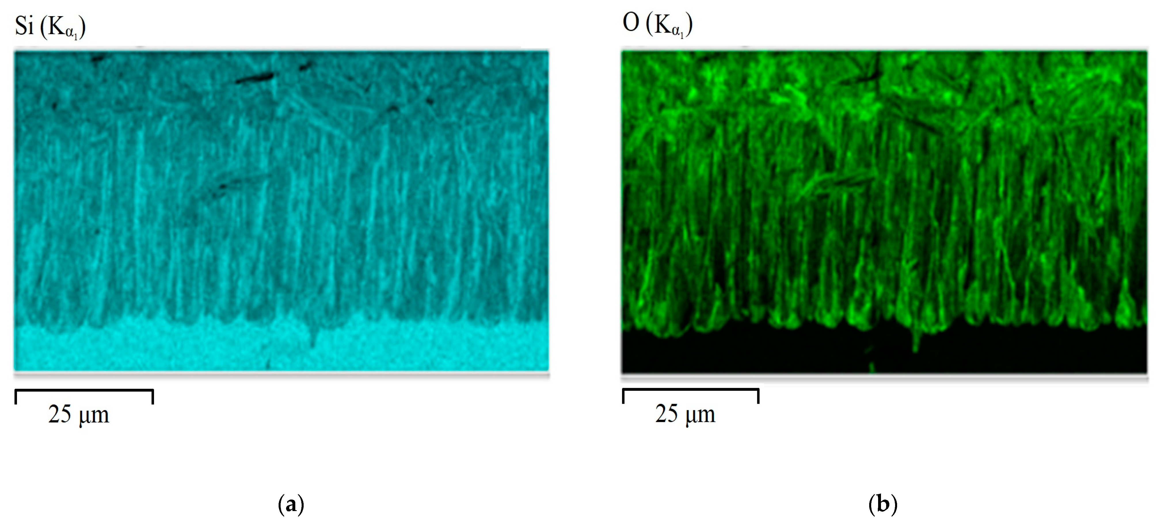
During the implementation of the first synthesis stage, a matrix of porous silicon was obtained. The results of studying the matrix by means of energy dispersive X-ray spectroscopy (EDS) and scanning electron microscopy are presented in
Figure 3 and
Figure 4, respectively.
According to the data shown in
Figure 3, a ~50 μm porous layer is formed on the silicon wafer surface. The resulting porous matrix is covered with a thin oxide layer. From the presented SEM images, the structure of the layer formed directly on the matrix of porous silicon is not visible, however, from our earlier studies [
10,
11] it is known that the surface of porous silicon immediately after the completion of the synthesis stage is covered with a high-resistivity surface thin oxide layer (also known as the “skin layer”), the existence of which is further supported by the results of energy dispersive X-ray spectroscopy investigation of the initial porous silicon matrix.
The thickness of the porous layer, characterized by a regular structure (
Figure 4b), reaches 50 μm, while the pores themselves are separated from each other by thin (no more than 200 nm) walls. The resulting structure, which is essentially an array of sharp tip field-emission cathodes, exhibits a high aspect ratio (no less than 100), which promotes effective enhancement of the electric field in the near-surface layer.
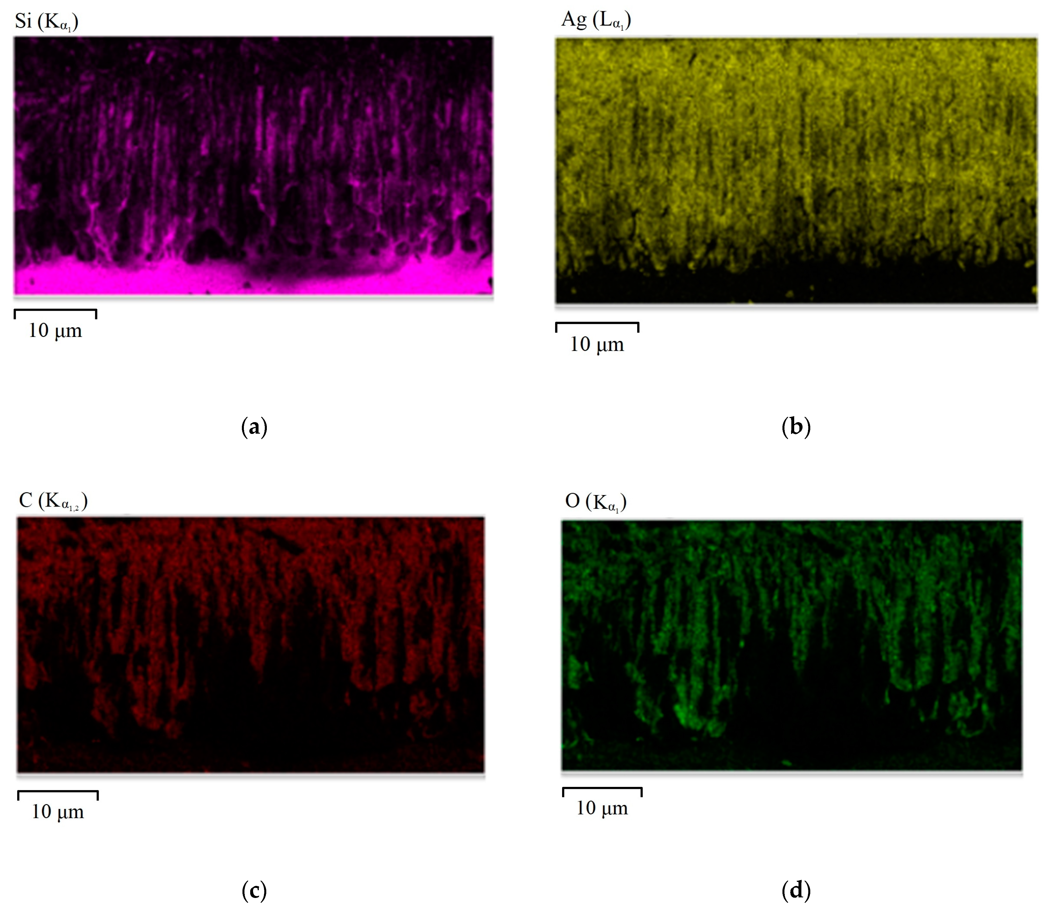
Figure 5 contains SEM images and EDS-obtained elemental distribution maps of the prototype cathode (porous silicon, functionalized with silver-doped carbon structures based on C
60) surface, obtained after the functionalization process occurred during the second stage of synthesis.
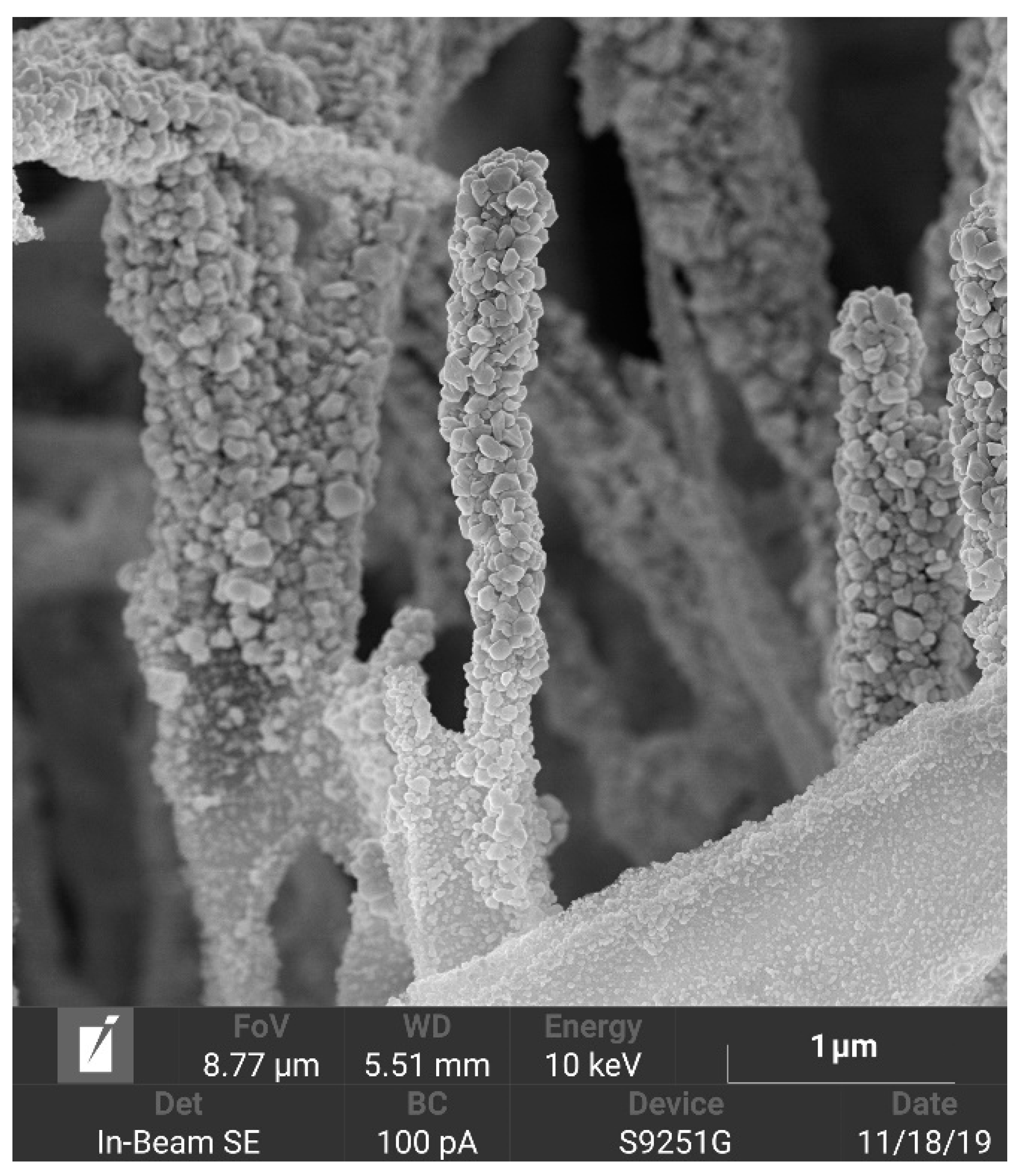
Figure 6 contains an SEM image of the prototype cathode cross-section at high magnification. As one can see from the figure, the initial PS surface at this stage is covered with a layer of C
60-based Ag-doped nanoscale aggregates with a mean size of 30 nm (with some of them being as large as approximately 100 nm), the elemental composition of which is supported by the results of energy dispersive X-ray spectroscopy shown in
Figure 5.
The analysis of elemental distribution maps acquired with EDS allowed us to detect signals from silver ( line) and carbon ( lines), in addition to the lines from Si and O already revealed during the analysis of the initial porous silicon matrix.
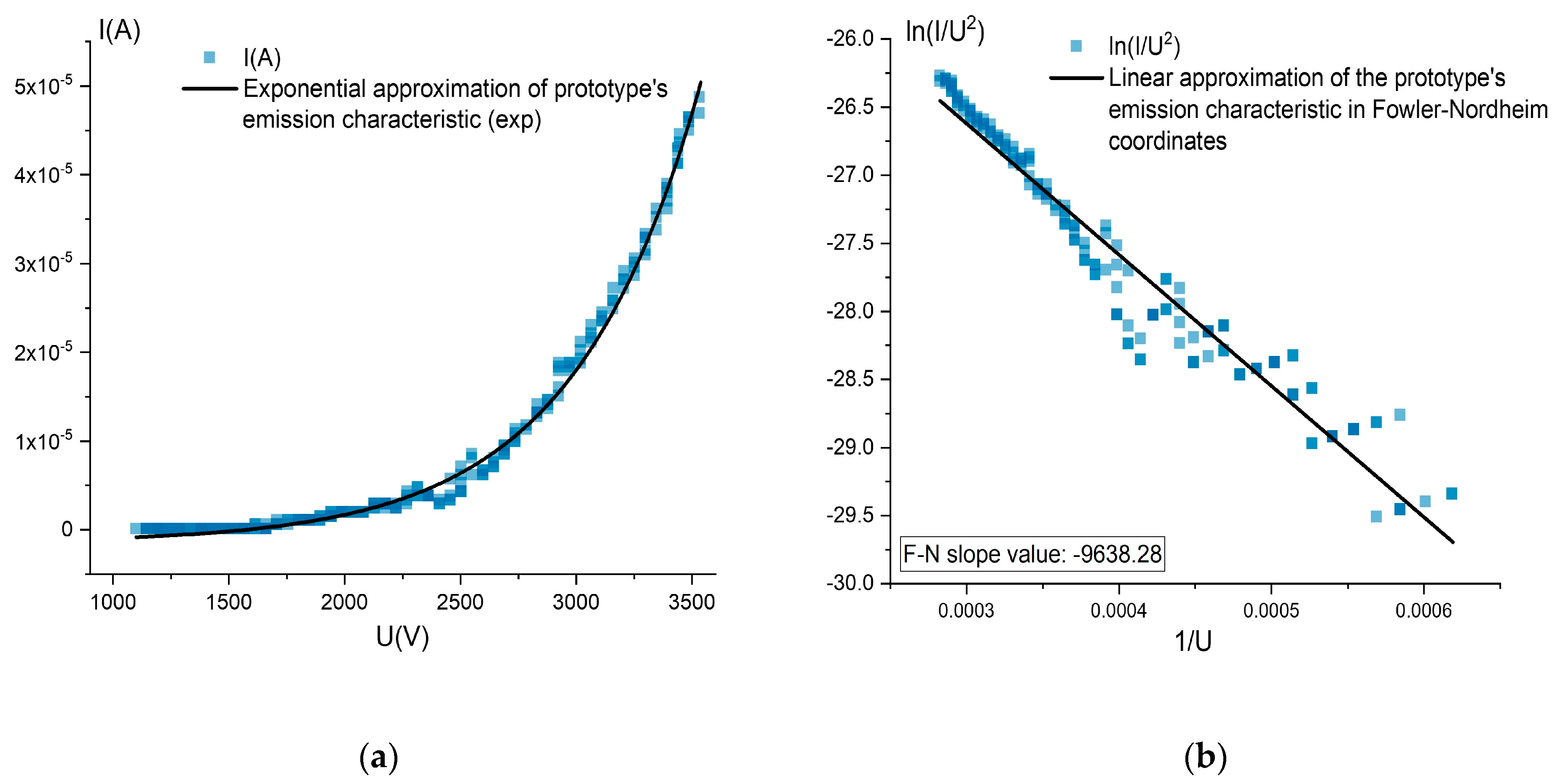
Some of the emission characteristics of the prototype are shown in
Figure 7. The exponential dependence of the electron current on the voltage applied between the cathode and the anode is clearly pronounced, which indicates the presence of field emission mechanisms. The threshold field strength was found to be 2.2 V/μm, the maximum applied field in the gap equaled 7.5 V/μm.
It should be noted that modern field emission cathodes based on monocrystalline silicon (n- and p-type) are characterized by threshold field strengths of the order of 1 V/nm (depending on the type of conductivity and doping level) [
9], which are at least three orders of magnitude higher than the values characteristic to those proposed in the study prototypes.
This effect is due to the presence of a low-macroscopic field emission phenomenon. In order to describe and analyze it, we proposed the model based on Anderson’s theory (later developed by Karpov [
33,
34]) regarding the existence of two-electron (2e) centers with negative correlation energy. In contrast to the previously considered (for example, in [
8]) ideas regarding the relationship between the process of dipole’s formation and imperfections of graphene-like layers’ crystal lattice, the model proposed in this study attempts to use the mechanism of low-macroscopic field emission to describe the process of electron emission from a wide range of carbon materials with a disordered structure (i.e., amorphous materials).
4. Discussion
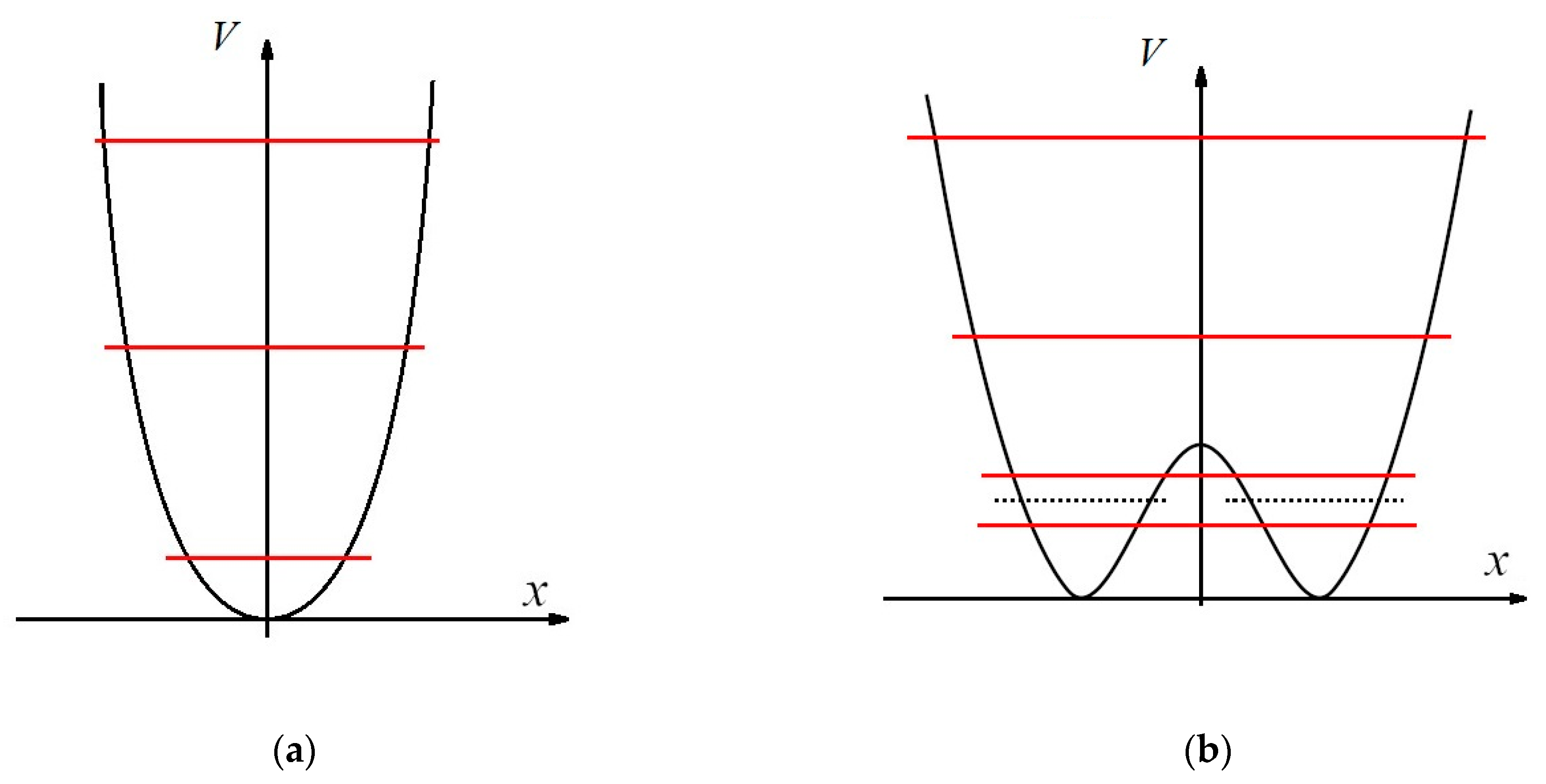
As a starting point for the emission model, one should consider the example of a two-well potential system in crystalline bodies with impurities or defects. When analyzing the potential energy of the displaced to the off-center position (relative to the ideal crystal lattice site) substitutional impurity atom, it is necessary to use the so-called two-well potential. Indeed, in this case, it is energetically more favorable for the impurity atom to be located in one of the off-center positions, the deviation of which can characterize the bond length in the amorphous body. At the same time, tunneling that occurs between two (or more) such states leads to the splitting of energy levels characterized by the same energy into two levels with close energy values (
Figure 8).
Thorough consideration of two-well potential emergence in amorphous bodies is presented in [
33,
34].
Figure 9 contains a schematic representation of the “central” atom’s potential in the field of two “neighbors” for a linear chain of three atoms. Here, provided that the distances between atoms 1 and 3 are small, atom 2 is located in a central position corresponding to the minimum value of its potential energy (
Figure 9a). A significant increase in the distance between atoms 1 and 3 leads to the modification of atom 2 potential, which starts being characterized by the presence of two minima, between which tunneling is possible (
Figure 9b).
For an amorphous body, the reason for such an increase lies in the effect of stretching of a particular chain by other atoms (which is confirmed, for example, by the excess of the volume of an amorphous body in relation to a crystalline one).
It should be noted that there is a certain value of the critical distance (and, accordingly, the critical potential) between atoms 1 and 3, at which there is a transition from a single-well potential to a two-well one (
Figure 9c). In this case, the sign of the second derivative of the atom 2 potential changes at the central point (
x = 0).
Thus, the critical potentials are characterized by small values of the second derivative. According to [
33,
34], this effect leads to the appearance of anomalously low values of the quasielastic constant, accompanied by an increase in the effective attraction between localized electrons and, consequently, the formation of states with a negative correlation energy.
As already noted, according to SEM and EDS data, the surface of the PS matrix is fully covered with an amorphous layer of nanosized (from 30 nm to 100 nm) aggregates of silver-doped carbon structures based on C
60 fullerene formed during functionalization. In this case, according to the idea put forward by the authors of [
7], each of the molecular aggregates of carbon nanostructures is isolated from the rest by tunnel barriers.
The estimate of dipole moment value for the obtained structure was carried out using the methodology proposed in [
8]. Hence,
, where
is the charge of the two-electron center,
is the mean size of a certain C
60-based aggregate (
Figure 6). The obtained values (
p = 9.6 × 10
−27 C·m) lead to the appearance of local fields with a strength of more than 10 V/nm under conditions of a relatively low macroscopic field (2.2 V/μm) and a high concentration of dipole moments. Indeed, the application of the dipole chain model [
35] is required in order to estimate the field strength in the form of (1):
where
p is the magnitude of the two-electron center dipole moment, C·m;
is the distance between the dipole centers, m;
is the electric constant, which leads to a value of
F = 15.4 V/nm. Thus, the magnitude of the local field strength near the emitter surface can reach and exceed 10 V/nm; that is, values sufficient to ensure the emission process.
The processing and analysis of emission characteristics were carried out using the method of Fowler–Nordheim-type graphical structures utilization [
28]. The functional connection in the modified coordinates is close to linear (the Pearson correlation coefficient ranged from −0.97 to −0.9, depending on the measurement cycle), thus indicating the presence of a field-induced emission mechanism.
The calculation of electron emission potential barrier height from the surface of the material was carried out according to the developed technique. Here we have (2):
where
a and
b are universal constants [
28],
AN is the total notional emission area,
H is the height of the potential barrier for electrons (eV),
γ is the local field enhancement factor,
r1 is the value of the generalized correction factor for the segment cut off on the coordinate axis (
r), and
s1 is the value of the generalized correction factor for the slope (
s); ln(
RM) and
SM, represent the values of the cutoff and the slope of the emission characteristic plotted in Fowler–Nordheim—type coordinates. According to Forbes [
28], the value of
s1 was taken equal to one.
As a result, the slope of the Fowler–Nordheim graph was represented in the following form (3):
In order to simplify the calculations, an expression equivalent to the one given in (3) was used for calculating the height of the electron emission potential barrier from the surface of the material utilizing the voltage (V) applied between the electrodes (rather than the field strength). Considering each correction factor, the expression could be written in the form (4):
where
d is the interelectrode gap value,
m,
γ is the local field enhancement factor (
γ = 100). The results of the calculation together with the acquired experimental data are summarized in
Table 1.
It should be noted that despite the processing of prototypes carried out according to the technique presented in the Materials and Methods section (namely, the removal of residual organics by heating the sample up to 200 °C.), the method we have implemented allows for some fluctuations in the measured emission characteristics, since the operation of low-macroscopic field emitters implies the existence of activation and deactivation processes for local emission centers [
36].
Owing to the optimal geometric configuration of porous silicon matrix that provides a high local field enhancement factor (γ no less than 100), as well as due to the presence of an amorphous silver-doped C60-based layer consisting of nanosized aggregates located on the matrix surface that ensure the low-macroscopic field emission mechanism conditioned by the formation of two-electron states with a negative correlation energy (the existence of which leads to a further increase in the local field strength), the prototype of the cathode exhibits emission properties that exceed those for classical semiconductor materials (including monocrystalline silicon).
The characteristics of promising samples of field-emission nanostructured cathodes known to date are presented in
Table 2.
The emitter prototypes obtained in the course of our studies are on par with or superior to modern and promising field emitters in a number of crucial parameters.
It should be noted that metallic field emitter arrays, despite the relative simplicity of the theoretical description and proven manufacturing technologies [
38], are very limited in terms of their application as current sources for nanoelectronic devices, primarily due to their incompatibility with complementary technologies for creating metal-oxide-semiconductor structures (CMOS), which are used to manufacture almost all modern integrated devices.
Field emission cathodes based on carbon nanotubes [
37] are characterized by diameters of individual structures ranging from 10 nm to 50 nm, with a packing density of 10
5–10
6 cm
−2. Despite the low values of the threshold field strength, due to still unresolved technological difficulties, it is rather challenging to fabricate arrays of identical nanotubes over a large area, and therefore the values of the emission current from cathodes of this type are comparatively small. It should be also noted that the prototype proposed in this study combines both the effect of local field enhancement due to specific morphology of its surface and the phenomenon of low-macroscopic field emission. Even though the phenomenon of low-macroscopic field emission is common to a wide range of materials [
28], the use of metal-doped nanostructures based on C
60 is more effective, since it turned out to be possible to acquire a uniform low-macroscopic field emission layer on the surface of a certain high aspect ratio matrix (in our case porous silicon acted as one). Although currently the technological process of fabricating large-scale carbon nanotube emission arrays presents certain difficulties, some progress has been achieved in this area [
40]. Still, the close proximity of nanotubes in these arrays leads to the appearance of such a spatial configuration of the near-surface electrostatic potential, that the effect of local field amplification virtually disappears.
In this regard, the developed prototypes are promising for the creation of high-intensity electron beams in low applied electric fields.
As already noted, modern field cathodes based on monocrystalline silicon (n- and p-type) are characterized by values of threshold field strengths of the order of 1 V/nm (depending on the type of conductivity and the doping level) [
9], thus demonstrating significantly worse emission properties than the prototypes developed in the course of this study.
Moreover, the presence of significant opportunities for doping of the molecular structures based on C
60 fullerene with a wide range of chemical elements not limited to silver suggests that the characteristics of the developed prototypes studied in this work can be significantly improved (for example, by using Cs as a doping element, an idea comprehensively realized in the field of thermionic emission, where the problems of electrode surface diagnostics [
7], as well as electron distribution function in plasma analysis, are crucial for its further development).
The obtained prototypes due to the low-macroscopic field emission effect occurring in them are superior in terms of emission characteristics (higher emission current density, lower threshold voltage) to regular cathodes based on porous silicon [
41,
42]. In regard to the use of pure C
60 as an emission coating, the studies carried out by the research group from St. Petersburg Polytechnic University have shown that such structures cannot be used as effective field cathodes due to their low stability under the prolonged influence of the electric field and the subsequent electrical breakdown [
43]. It should be also noted that the emission characteristics demonstrated by pure C
60 films are inferior to those of the materials proposed in this study, both in terms of threshold voltage (8 kV for pure C
60 instead of 1.1 kV for our prototypes) and emitted current density (2.5 × 10
3 μA/cm
2 for pure C
60 instead of 6.28 × 10
3 μA/cm
2 for our prototypes) [
44].
