1. Introduction
Microstrip patch antennas have been widely used in the past years thanks to key features, such as low profile, light weight, ease of integration with planar circuits, and low-cost manufacturing [
1]. Such advantages become particularly relevant when several patches are arranged in an array configuration to realize high gain antennas with properly shaped radiation patterns. For this reason, microstrip array antennas are appealing for most of modern communication, radar, and remote sensing systems.
On the other hand, due to their resonant properties, microstrip patch antennas may be affected by a narrowband behavior. In fact, the impedance bandwidth of a microstrip patch, depending on its substrate parameters and thickness, typically reaches only a few percent fractional bandwidth, and this is a critical limit in wideband applications. As a consequence, techniques and architectures focusing on bandwidth broadening are of great interest for modern microwave systems.
The substrate parameters directly influence the antenna bandwidth. In fact, the microstrip patch and the ground plane can be intuitively seen as a capacitor, where the stored energy increases by increasing the substrate dielectric constant and reducing its thickness. By doing so, the merit factor of the resonator increases, and the antenna bandwidth is reduced. As a consequence, a low permittivity substrate with high thickness is recommended for a broadband behavior.
While decreasing the substrate dielectric constant is feasible, as it depends only on the material choice, an increased thickness can lead to some disadvantages. In fact, the patch higher-order modes may be excited, causing radiation pattern degradation, especially in large arrays. Moreover, surface waves can be generated, thus increasing the mutual coupling between elements in an array environment, potentially causing scan blindness. In addition to this, when using a transmission line feed, a thick substrate requires a wider line, thus leading to a more difficult routing and to a significant leakage in the beam forming network (BFN). Finally, a thick substrate increases the antenna volume as well as its weight and cost.
Many approaches have been introduced in recent books [
2,
3,
4,
5,
6] and articles to extend the bandwidth of a microstrip patch antenna up to 50% and more, nevertheless, this always comes as a trade-off, either in gain, polarization, or complexity of the antenna configuration. There is a vast literature on broadband patch antennas: some techniques include two-layer proximity-coupled patches [
7,
8], aperture-coupled patches [
9,
10], and stacked patches [
11,
12,
13]. These solutions increase the manufacturing complexity and cost, as all of them require multilayer substrates. However, the use of a single-layer substrate may be required in certain low-cost broadband applications.
To this purpose, the multiple-resonance concept is employed, which consists in the introduction of additional resonances close to the resonant frequency of the patch antenna. Among the numerous works, the most known are slotted patches [
14,
15,
16,
17,
18], E-shaped patches [
19,
20], capacitively-coupled patches [
21], and patches fed by shaped probes [
22,
23,
24]. It is worth mentioning that the majority of these designs need a thick foam substrate or an air gap, thus leading to a more difficult assembling phase. In addition to this, all the patches are fed by coaxial probes, and this approach requires the use of an additional layer for the BFN in all array implementations.
In order to minimize the cost of a broadband microstrip patch array antenna, single-layer line-fed patches on thin substrates must be considered. In fact, a thin dielectric is lighter and cheaper. Moreover, the antenna elements and the feeding network can be integrated on the same substrate, thus making it possible to adopt a standard printed circuit technology, avoiding the use of multilayer techniques. Nevertheless, only a few works have been reported on this subject. An impedance-matching network realized as two parallel line stubs is found in [
25], though the need for the additional resonators could be a limit in the design of feeding networks for large arrays. A tooth-like-slot patch antenna is presented in [
26]. This solution is not straightforward due to many geometrical parameters involved, moreover, a quarter-wave transformer is needed, and a thick substrate is adopted. Broadband operation of triangular patch antennas by means of properly bent slots is examined in [
27], where good performance is achieved with a reduced number of geometrical variables. Two quarter-wave resonators with a shorting pin are adopted in [
28] to capacitively feed a patch antenna for wideband radiation under dual resonance. Although promising results can be obtained, the via hole insertion complicates the manufacturing process. Proximity-coupled patch antennas can also be designed on a single layer as in [
29], where a broadband circularly polarized element is obtained by just acting on the feeding method.
In this paper, two configurations of line-fed broadband microstrip patch antennas on a single-layer thin substrate are presented. A 50-ohm line is used to realize an inset feed and its small width is indeed suitable for the design of printed array BFNs on the same layer of the radiating elements. A merit factor based on the design center frequency, element dimensions, and substrate parameters is introduced to provide a fair comparison between solutions with similar characteristics. Two patch antenna inexpensive prototypes are fabricated using a low-cost computer numerical control (CNC) milling machine and an in-house etching process. All simulations are performed using the full-wave software CST Microwave Studio. All antenna geometries are optimized with the CST built-in genetic algorithm. Measured results show very good agreement with the simulations.
2. Microstrip Patch Antenna Design
Two configurations of microstrip patch antennas are shown in
Figure 1, which will be referred to as MPA1 and MPA2. The former is a standard patch antenna with an inset feed, the latter is an inset-fed patch antenna with a symmetrical pair of cuts along its width. Both antennas are designed at a center frequency of 10 GHz on a thin layer of Rogers RT5880 substrate (
h = 0.508 mm,
t = 35 µm,
εr = 2.2, tan
δ = 9 × 10
–4 at 10 GHz) and fed by a 50-ohm transmission line, whose width is
w = 1.51 mm.
Geometrical parameters for MPA1 and MPA2 are listed in
Table 1. For manufacturing reasons, all inset gap widths are fixed and equal to
g = 0.50 mm. It will be shown that a broader bandwidth can be achieved as the gap widths are reduced. Both antenna geometries are the result of a full-wave optimization. Simulated reflection coefficient is shown in
Figure 2 for both antennas.
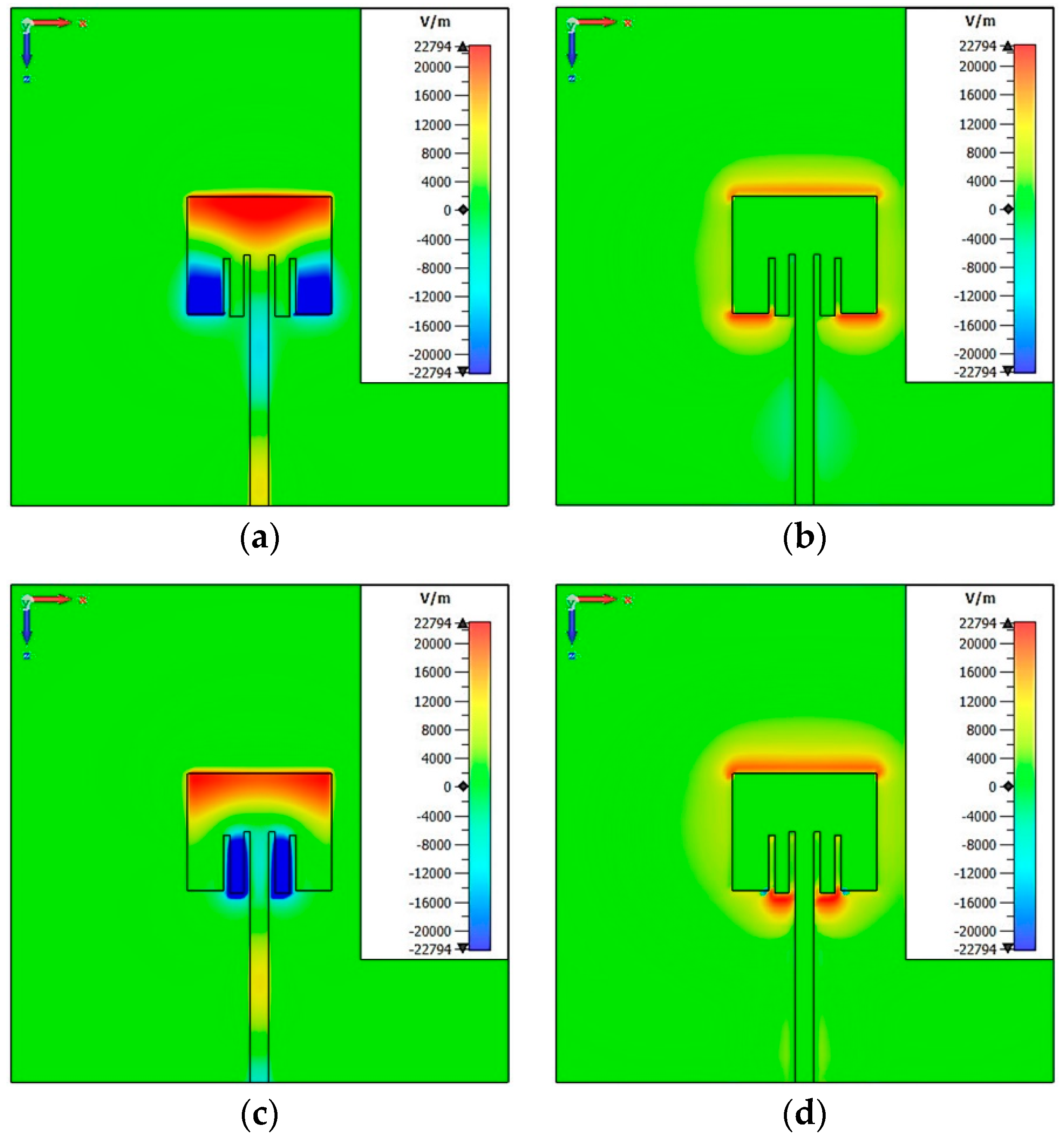
Due to its resonant properties, MPA1 presents a narrow 10-dB reflection coefficient bandwidth ranging from 9.926 GHz to 10.085 GHz, corresponding to a 1.59% fractional bandwidth (FBW). On the contrary, MPA2 10-dB reflection coefficient bandwidth extends from 9.821 GHz to 10.162 GHz, which is equal to a 3.41% FBW. The reflection coefficient curve for MPA2 shows two resonances at 9.880 GHz and 10.120 GHz and despite a slightly worse matching at center frequency, the overall bandwidth is broadened with respect to the case of MPA1 by a factor of 2.14. The y- and z-components of the electric field at 9.880 GHz and 10.120 GHz are plotted in
Figure 3. The E-field plots highlight the active regions on the patch edges at the two resonance frequencies.
In particular,
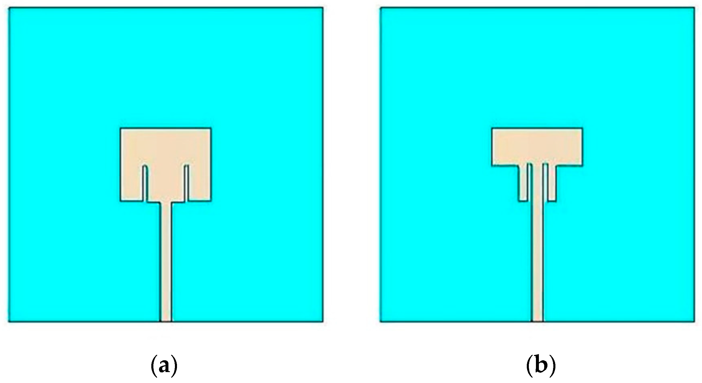
Figure 3 suggests that MPA2 could be seen as the combination of two distinct patch antennas resonating at different frequencies, close enough to result in a bandwidth broadening. To verify this statement, two configurations of sub-patches originating from MPA2 are extracted and illustrated in
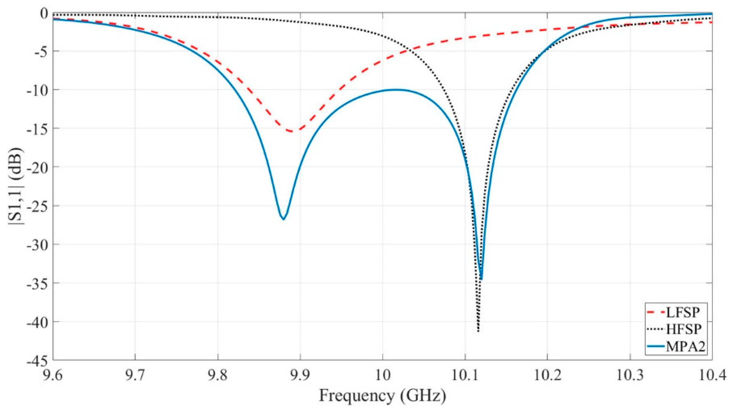
Figure 4.
The low- and high-frequency sub-patches resonate at the same frequencies exhibited by MPA2, as clearly shown in
Figure 5. These results prove that MPA2 is indeed the superposition of two independent patch antennas.
It is worth mentioning that, even though the geometry is similar to the one of E-shaped patch antennas, the design approach and basic principle adopted in this work are different. In fact, instead of referring to the patch resonant modes, the overall structure is modeled as a combination of traditional single-resonance geometries. In addition to this, to the authors’ knowledge, the vast majority of E-shaped patch antennas are coaxial-fed and, in the case of transmission line feeding, the microstrip inset is located on the opposite side of the pair of cuts.
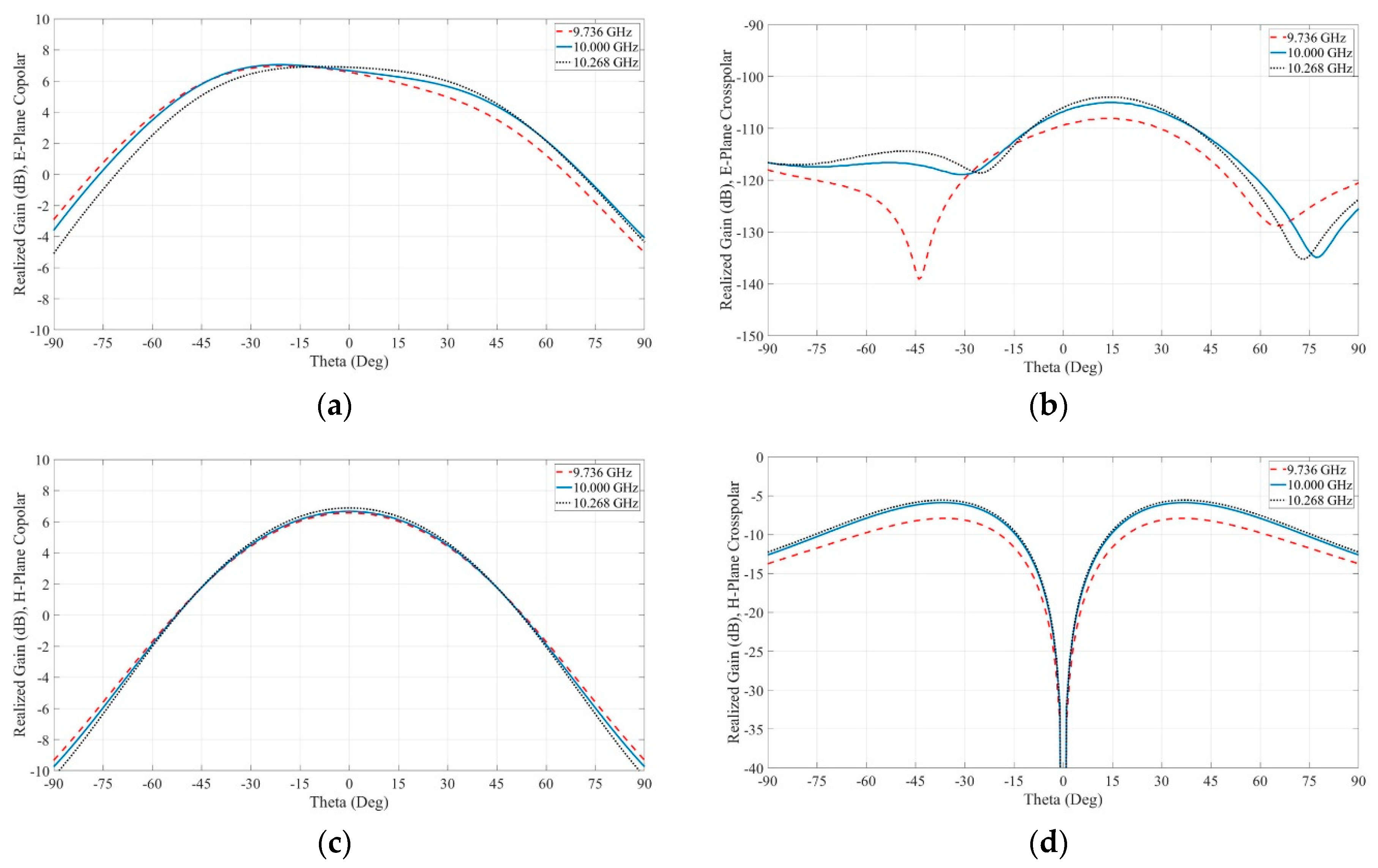
The E-plane and H-plane radiation patterns are reported in
Figure 6 at 10 GHz and at the lower and higher frequencies of the 10-dB reflection coefficient bandwidth. The antenna radiates a linearly polarized electric field with the typical hemispherical distribution of microstrip patch antennas. A very stable copolar beamwidth is observed, with low cross-polarization levels over the whole operative band, making this radiating element particularly suitable for array applications.
With the purpose of further improving the reflection coefficient bandwidth, a further patch antenna is designed and shown in
Figure 7. This antenna, namely MPA3, is the combination of three resonating structures, thus presenting two symmetrical pairs of cuts along its width. This antenna is fed by the same 50-ohm transmission line and all inset gap widths are fixed and equal to
g = 0.50 mm for manufacturing reasons. Geometrical parameters are the result of a full-wave optimization and are listed in
Table 2. Simulated reflection coefficient for MPA3 is shown in
Figure 8.
The reflection coefficient bandwidth extends from 9.736 GHz to 10.268 GHz, which is equal to a 5.32% FBW. The reflection coefficient curve shows two resonances at 9.808 GHz and 10.180 GHz and, despite a slightly worse matching at center frequency, the overall bandwidth is broadened with respect to the case of MPA1 by a factor of 3.35. A third resonance can be observed, although not visible in
Figure 8 being outside the frequency range of interest. Nevertheless, the introduction of a third resonator is indeed functional to the bandwidth broadening at 10 GHz.
The E-plane and H-plane radiation patterns are reported in
Figure 9 at 10 GHz and at the lower and higher frequencies of the 10-dB reflection coefficient bandwidth. The antenna radiates a linearly polarized electric field, again with the typical hemispherical distribution of microstrip patch antennas with stable performance and low cross-polarization.
The broadside gain versus frequency is depicted in
Figure 10 for all radiating elements. Compared to the traditional patch antenna, MPA2 and MPA3 exhibit a flat range around center frequency. Despite the very low profile of the adopted dielectric material, for all proposed elements, a simulated radiation efficiency above 80% is observed in the operative frequency band.
Two modified versions of MPA2 and MPA3, namely MPA4 and MPA5, fed by the same 50-ohm transmission line, clearly highlights the impact on the antenna performance of the inset gap width now set equal to
g = 0.25 mm. The remaining geometrical parameters are the result of a full-wave optimization and are listed in
Table 3.
Simulated reflection coefficient characteristics for MPA4 and MPA5 are reported in
Figure 11 and
Figure 12 to show the bandwidth broadening caused by the reduced gap widths with respect to MPA2 and MPA3. The MPA4 reflection coefficient bandwidth extends from 9.747 GHz to 10.268 GHz, which is equal to a 5.21% FBW. The MPA5 reflection coefficient bandwidth extends from 9.656 GHz to 10.342 GHz, which is equal to a 6.86% FBW.
In addition to this, to further highlight the potentiality of the illustrated antennas, MPA2 is redesigned using a substrate of doubled thickness, which is
h = 1.016 mm. This antenna, namely MPA6, is fed by a 50-ohm transmission line, whose width is
w = 3.00 mm. All inset gap widths are fixed and equal to
g = 0.50 mm. The remaining geometrical parameters are the result of a full-wave optimization. Geometrical parameters and simulated scattering parameters are shown in
Table 4 and
Figure 13, respectively.
The 10-dB reflection coefficient bandwidth for MPA6 extends from 9.591 GHz to 10.388 GHz, which is equal to a 7.98% FBW. This means that the antenna bandwidth is increased by a factor of 2.16 with respect to MPA2 using a substrate of doubled thickness, as expected from microstrip antenna theory.
3. Microstrip Patch Antenna Manufacturing and Test
The three illustrated antennas are manufactured using a fast in-house prototyping process comprising a low-cost printed circuit board (PCB) milling machine and a traditional etching solution. The milling machine is controlled with computer-aided manufacturing (CAM) software. In order to guarantee high accuracy machining, a two-step calibration phase is required. The first step is the depth calibration of the milling tool, which is a V-shaped drill used as a conductive probe to sample the PCB in a number of points in order to obtain a numerical profile of the surface where the milling takes place. By doing so, it is possible to keep the milling tool at a constant depth along the vertical axis, drilling only the copper layer and leaving the substrate almost untouched. The second step is the groove width calibration, which consists in milling a test pattern of known dimensions. A microscope is used to measure the groove width and, if necessary, a correction of the CAM software parameters is applied to minimize the manufacturing errors. Machining is performed at low speed in order to have a clear cut on the copper layer. A cooling process must be adopted to dissipate the heat generated by the friction of the milling tool during the drilling process. To this purpose, a thin layer of water is used to cool the drill and mitigate any thermal deformation, as shown in
Figure 14. In this way, an almost constant groove width can be guaranteed with a tolerance of ±10 µm. In addition to this, the water layer avoids the dispersion of thin particles in the air. In order to minimize the machined surface area and to speed up the entire manufacturing process, the antenna pattern is contoured with a milled groove of 1–1.5 mm, then protected with a thin layer of nail varnish and finally etched using a ferric chloride solution to remove the remaining copper.
The three prototypes, shown in
Figure 15, are tested with an Agilent N5230A vector network analyzer using the one-port short-open-load calibration technique. Measured results are compared with simulations and, despite minor frequency shifts caused by manufacturing tolerances, a very good agreement can be observed in
Figure 16. The 10-dB measured reflection coefficient bandwidth for MPA1 extends from 9.867 GHz to 10.050 GHz, which is equal to a 1.84% FBW. The 10-dB measured reflection coefficient bandwidth for MPA2 extends from 9.844 GHz to 10.216 GHz, which is equal to a 3.71% FBW. The 10-dB measured reflection coefficient bandwidth for MPA3 extends from 9.702 GHz to 10.314 GHz, which is equal to a 6.12% FBW.
In order to fully understand the importance of such results, the performance of MPA1, MPA2, MPA3, MPA4, MPA5, and MPA6 are compared with patch antenna designs of similar characteristics, which are the line-fed radiating elements printed on single-layer thin substrates [
25,
26,
27,
28,
29]. A merit factor must be introduced to take into account the design center frequency, element dimensions, and substrate parameters.
It is well known that the microstrip patch antenna bandwidth is related to the free-space wavelength, the substrate height, the width-to-length ratio and the dielectric constant as follows [
30]:
It is, therefore, reasonable to normalize the effects of the above-mentioned parameters by introducing a merit factor
F in the form of:
where
BW is the 10-dB measured antenna bandwidth. All single-layer line-fed broadband patch antenna designs are compared in
Table 5. In order to highlight an actual bandwidth improvement, each merit factor is also normalized to the highest state-of-the-art merit factor, corresponding to reference [
26]. Simulated results for MPA4, MPA5, and MPA6 are considered, as measured data are not available. A reduced copper conductivity of
σ = 10
7 S/m is estimated in the simulations to account for any surface roughness.
It is evident that MPA3 exhibits the highest measured merit factor among all works. MPA2 achieves very good performance, comparable to the one of [
29] for a circularly polarized patch antenna. Moreover, MPA4, MPA5, and MPA6 show remarkable results, each with a merit factor greater than the one of [
26]. In particular, MPA4 achieves the highest simulated merit factor as a consequence of the width reduction of the inset gaps, as mentioned in the previous section.


