Article

Design of a Real-Time Breakdown Voltage and On-Chip Temperature Monitoring System for Single Photon Avalanche Diodes

1
School of Electronic Engineering and Automation, Guilin University of Electronic Technology, Guilin 541004, China
2
Guangxi Key Laboratory of Optoelectronic Information Processing, Guilin University of Electronic Technology, Guilin 541004, China
3
Department of Electrical and Electronic Engineering, University College Cork, T12 YN60 Cork, Ireland
*
Authors to whom correspondence should be addressed.
Electronics 2021, 10(1), 25; https://doi.org/10.3390/electronics10010025
Submission received: 11 November 2020 / Revised: 6 December 2020 / Accepted: 23 December 2020 / Published: 27 December 2020
(This article belongs to the Section Microelectronics)

Abstract

:
The design and implementation of a real-time breakdown voltage and on-chip temperature monitoring system for single photon avalanche diodes (SPADs) is described in this work. In the system, an on-chip shaded (active area of the detector covered by a metal layer) SPAD is used to provide a dark count rate for the breakdown voltage and temperature calculation. A bias circuit was designed to provide a bias voltage scanning for the shaded SPAD. A microcontroller records the pulses from the anode of the shaded SPAD and calculates its real-time dark count rate. An algorithm was developed for the microcontroller to calculate the SPAD’s breakdown voltage and the on-chip temperature in real time. Experimental results show that the system is capable of measuring the SPAD’s breakdown voltage with a mismatch of less than 1.2%. Results also show that the system can provide real-time on-chip temperature monitoring for the range of −10 to 50 °C with errors of less than 1.7 °C. The system proposed can be used for the real-time SPAD’s breakdown voltage and temperature estimation for dual-SPADs or SPAD arrays chip where identical detectors are fabricated on the same chip and one or more dummy SPADs are shaded. With the breakdown voltage and the on-chip temperature monitoring, intelligent control logic can be developed to optimize the performance of the SPAD-based photon counting system by adjusting the parameters such as excess bias voltage and dead-time. This is particularly useful for SPAD photon counting systems used in complex working environments such as the applications in 3D LIDAR imaging for geodesy, geology, geomorphology, forestry, atmospheric physics and autonomous vehicles.

1. Introduction

Single photon counting technology has been used in a wide range of low light sensing applications such as LIDAR [1,2], DNA sequencing [3], quantum key distribution [4] and medical imaging [5,6] due to its ultra-high sensitivity and photon counting capability. Traditionally, single-photon detection systems use photomultiplier tube (PMT) or micro-channel plates (MCPs) as the detector. These are normally expensive, bulky (requires a relatively large vacuum tube to operate), requires high bias voltages, are sensitive to magnetic fields, and difficult to integrate with electronic circuits [7,8,9]. Over the past decade, single photon avalanche diodes (SPADs) have been widely used to replace the PMT and MCPs in photon counting applications. This is mainly due to its lower operating voltage, smaller size, lower power consumption, insensitivity to electromagnetic noise, and easy integration with electronic circuits [10,11,12,13]. The breakdown voltage of SPADs is the voltage corresponding to the critical breakdown of SPADs and the excess bias voltage of the SPAD is the additional voltage above the breakdown where the device is typically biased. This has a major effect on the SPAD’s performance parameters such as the dark count rate (DCR) and photon detection efficiency (PDE). Higher excess bias voltage will lead to better PDE due to the increase in the avalanche triggering probability. However, the trade-off includes a higher DCR and a significant after-pulsing effect (both resulting in false photon detection counts). Therefore, the breakdown voltage should be precisely monitored to allow setting an optimal excess bias voltage for overall performance optimization. In practical applications, some key performance parameters (including dark count rate, breakdown voltage and after-pulsing) of SPADs are also affected by the temperature which should also been monitored. Existing methods for measuring breakdown voltage requires benchtop instruments for bias voltage scanning and counting rate/current recording and analysis. These methods are complex and cannot provide the real-time measurement of breakdown voltage in a time-varying environment [14,15,16,17]. Temperature sensors are normally used to monitor the temperature of the photon counting system. However, this approach does not measure the detector chip temperature directly, only that of the surrounding package, leading to significant errors in the measurement (when the detector is under illumination, the on-chip and off-chip temperatures will be different).
In this work, a real-time breakdown voltage and on-chip temperature monitoring system for the SPAD is designed. In the system, an on-chip shaded SPAD is used which is covered by a layer of metal and kept in the dark. This SPAD measures only a dark count rate in response to changes in bias voltage and temperature. A bias circuit that works under microcontroller control was designed to sweep the bias voltage to the SPAD with a high resolution of 10 mV. A signal conditioning circuit was designed to convert the output of the SPAD to standard transistor-transistor logic (TTL) pulses. The microcontroller circuit records these pulses and calculates the real-time dark count rate of the SPAD. An algorithm was developed and implemented on the microcontroller to calculate the real-time breakdown voltage and the on-chip temperature of the SPAD. Experimental results show that the system is capable of measuring the SPAD’s breakdown voltage with the error of less than 1.2% and on-chip temperature error of less than 1.7 °C in the range of −10–50 °C. This system can be used for real-time breakdown voltage and temperature estimation for the dual-SPADs or SPAD arrays where identical detectors are fabricated on the same chip and one or more dummy SPADs are shaded. Based on the breakdown voltage and the on-chip temperature measured, intelligent control logic can be developed to optimize the performance of the SPAD based photon counting system by adjusting the parameters such as the excess bias voltage and dead-time. This is particularly useful when the photon counting system is used under a complex working environment such as the applications in 3D LIDAR imaging for geodesy, geology, geomorphology, forestry, atmospheric physics and autonomous vehicles.

2. System Description

Figure 1 shows the block diagram of the system proposed which mainly consists of: 1. A power management circuit that supplies appropriate power for different components; 2. A microcontrolled bias circuit that produces a wide range and high resolution sweeping voltage to the SPAD; 3. A SPAD chip with one signal SPAD and one shaded SPAD biased by the bias circuit and its output connected to the signal conditioning circuitry; 4. Signal conditioning circuitry which consists of an resistor connected in series with the SPAD for passive quenching and a comparator used to convert the output of the SPAD to TTL signal; 5. A microcontroller (STM32F103C8T6, STMicroelectronics, Geneva, Switzerland) based system is used for the counting rate calculation using the pulses from the signal conditioning circuitry, bias voltage setting and scanning, the breakdown voltage and on-chip temperature calculation and results reporting.

2.1. Power Management and Bias Voltage Setting Circuitry

Figure 2 shows the schematic of the power management (Figure 2a) and bias circuit (Figure 2b). The power management circuit is powered by a high input voltage (Vhigh), which is also the power supply for the buck circuit in the bias circuit. This determines the upper limit of the scanning bias voltage which can be set up to 600 V. In the power management circuit, three step-down DC–DC converter integrated circuits (LM2576HV-12 (Texas Instruments, Dallas, TX, USA), LM7805 (Texas Instruments, Dallas, TX, USA), AMS1117-3.3 (Advanced Monolithic Systems, Livermore, CA, USA)) are used to convert the high input voltage to +12 V, +5 V and +3.3 V which are used to power the components in the bias circuit, the signal shaping (conditioning) circuit and also the microcontroller.
In the bias circuit, an optocoupler (6N137, Vishay, Malvern, PA, USA) is used to prevent the direct connection between the I/O pin of the microcontroller and the high-power driving chip and to prevent the large reverse current flowing back to the microcontroller. A half-bridge driver (IR2104, Infineon Technologies, New Biberg, Germany) is used to enhance the driving capability of the PWM signal from the microcontroller. In the buck circuit, two N-channel MOSFETs (NMOS1 and NMOS2) connected in series with an inductor and a capacitor are used for the energy charging and discharging and also used as a low pass filter to reduce the ripple at the output. At the output, R1 and R2 are used to reduce the output voltage to a low level which will be used as the feedback voltage and exported to the microcontroller through an analog-to-digital converter (ADC). In the circuit, when NMOS1 is on and NMOS2 is off, the output is charging and the output voltage increases. When the NMOS1 is off and NMOS2 is on, the output discharges through NMOS2 which decreases the output voltage. The microcontroller senses the output voltage level and adjusts the duty cycle of the PWM signal accordingly. The on and off time of NMOS1 and NMOS2 is adjusted by the half-bridge driver chip according to the PWM signal. The output voltage to the SPAD is then adjusted to achieve the operating voltage. The resolution of the output voltage is decided by the frequency of the PWM signal and the ADC resolution, in our design, a setting step of 10 mV is achieved.

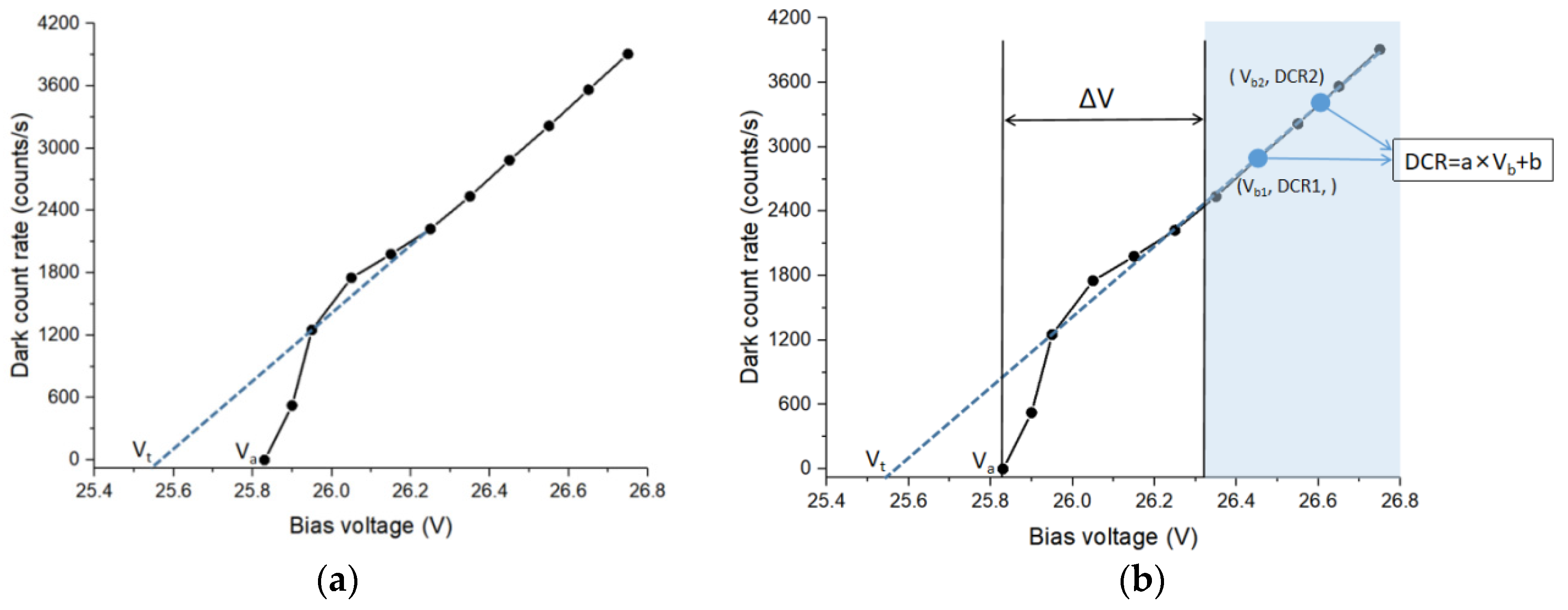
2.2. Breakdown Voltage and Temperature Calculation

The breakdown voltage is the bias voltage at which SPAD’s electric field strength generated in the depletion region is sufficient to initiate avalanche breakdown in the presence of a charged carrier. To measure the breakdown voltage, a bias voltage sweep is conducted on the shaded SPAD and its corresponding dark count rate is recorded by the microcontroller. The SPAD’s apparent breakdown voltage (Va) is different from the true breakdown voltage (Vt), see Figure 3a. The apparent breakdown voltage cannot accurately reflect the true state of the SPAD as it can be easily affected by the trigger level used to sense the pulses at the output of the SPAD. At a small excess of bias voltage (bias voltage–breakdown voltage), the breakdown current is small and the corresponding pulses can be easily affected by the voltage noises at the anode of the SPAD.
To achieve the measurement of the true breakdown voltage, the following steps are used and implemented on the microcontroller: 1. Sweeping the bias voltage, calculate the shaded SPAD’s counting rate to find the apparent breakdown voltage (when the counting rate is just above 0). A binary search algorithm is used to speed up the process. Initially the bias voltage is set to the mid-point of the initial voltage setting range (Vo, the maximum bias voltage estimated might be applied to the SPAD, in this work the “initial voltage setting range” Vo is set to the 30 V) and the SPAD counting rate is recorded. If no counting is observed from the signal shaping circuit, then the voltage sweep is set in the range to Vo/2–Vo and the first step is repeated. If a high counting rate is observed, then the searching range is set to 0–Vo/2 and the first step is repeated. In this way, the apparent breakdown voltage (Va) can be found; 2. Record two points (Vb1, DCR1) and (Vb2, DCR1) in the linear response region. The setting bias voltages, Vb1 and Vb2, should be greater than Va + ∆V, where ∆V in this case is set to 0.5 V to make sure the two points are taken in the linear region. By using the two data points, a linear expression of the DRC and Vb can be derived and by setting the DCR to 0 in the expression, the true breakdown voltage (Vt) can be calculated, see Figure 3b. For the on-chip temperature monitoring, a series of temperature versus true breakdown voltage data are recorded and plotted. A linear fit to the data is produced and the fitting results are used and pre-implemented on the microcontroller. In the system, once the true breakdown voltage is calculated, it is sent to the temperature calculation algorithm and the real-time on-chip temperature can be measured (using the pre-implemented fitting data and currently measured true breakdown voltage). To improve the accuracy of the temperature measurement, 10 real-time temperatures are measured and their average value is used as the result.

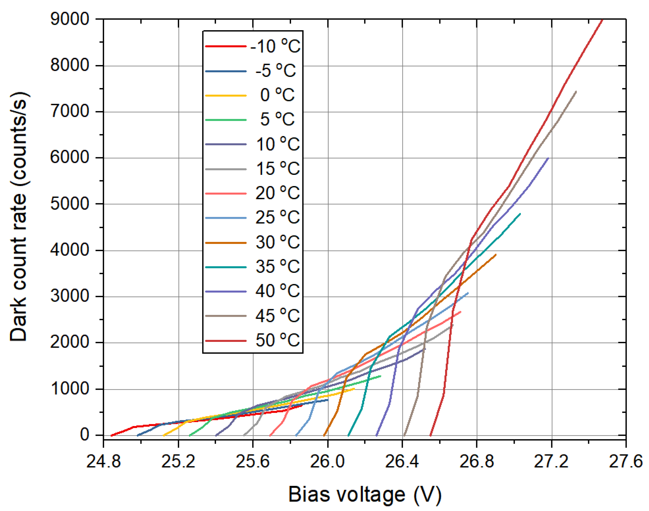
3. Experimental Results

In the system, a previously developed dual-SPAD chip is used and a photograph of the chip can be seen in Figure 4a. On the dual-SPAD chip, two 20 µm planar SPADs [18,19] are fabricated with one exposed to the light and the other one covered by a metal layer which is used for the breakdown voltage and on-chip temperature monitoring. The SPAD’s structure consists of a p-substrate with a p-type doping forming the central active area and the N+ doping overlaps the active area, forms the diode cathode. The overlapping guard ring, and the diode it forms with the p-substrate, prevents the edge breakdown of the central active area. A high dose P+ implant on the detector’s periphery is used for top contact to the anode providing a planar device, which allows flip chip integration. The board developed for the proposed system can be seen in Figure 4b. In the experiments, a temperature chamber is used to vary the temperature applied on the SPAD chip which is placed inside the chamber with its mounting board. A DC power supply is used to provide the high voltage, Vhigh (about 60 V which can be set to higher voltage when required) to the whole system that allows the bias voltage setting range from 0 to around 55 V (the efficiency of the buck circuit is about 92%). We initially measured the breakdown voltage of the SPAD using bench top instruments including power supply and a counter (FCA3100, Tektronix, Beaverton, OR, USA). Then, we measured the SPAD’s breakdown voltages using the system developed in this work for comparison. For the temperature measurement, we use the system developed to measure real-time on-chip temperatures and compare them with the setting temperature of the temperature chamber.
Figure 5 shows the dark count rate measured on the shaded SPAD under different bias voltages (using bench top instruments) and various temperatures. By implementing a linear fitting on the linear region of each plot, the true breakdown voltages on the SPAD versus temperatures can be plotted which is shown in Figure 6. A linear fit is used and the relationship between the breakdown voltage and the temperature is established. This expression is implemented on the microcontroller and used for the on-chip temperature measurement.
Figure 7 shows the real-time measurement results of the breakdown voltages on the SPAD using the system developed for various temperatures. The breakdown voltages measured by the bench-top instruments are also plotted for comparison. Results show that the system is able to measure the SPAD’s true breakdown voltage in real-time with a maximum mismatch of around 0.3 V, corresponding to an error of around 1.15% compared to the breakdown voltage measured by the bench-top instruments.
Figure 8 shows the evolution of the on-chip temperature calculated by the system for different setting temperatures. The measured temperatures present the same trend as the setting temperatures, see Figure 8a. The maximum mismatch measured is about 1.7 °C (Figure 8b). This is mainly caused by the measurement mismatch of the breakdown voltage. In addition, the setting variations of the temperature chamber also contributes additional mismatches on the temperature.
To test the stability of the t system, we kept the system continuously running for more than 100 h, at two temperatures of −5 and 35 °C. Results can be seen in Figure 9, which show that the system did not show any obvious drift in the measurement results.
When the device is implemented for the SPAD arrays, it might be affected by the process variations. The potential improvement solution for this is that in the SPAD arrays, some shaded SPADs will be selected, which should be distributed around the whole SPAD arrays chip as shown in Figure 10 to alleviate the affection of the process variations. The shaded SPADs’ dark count rates will be recorded, averaged and used for the temperature monitoring of the overall SPAD arrays chip and breakdown voltage estimation.

4. Conclusions

In this work, a real-time breakdown voltage and on-chip temperature monitoring system for the SPAD was designed. In the system, a shaded SPAD was used to provide a dark count rate for the real-time breakdown voltage and temperature monitoring. A bias circuit was designed to provide a voltage sweep (under the control of a microcontroller) to the SPAD with a resolution of 10 mV. A pulse shaping circuit was used to convert the output pulses to standard TTL pulses. The microcontroller circuit records these pulses and calculates the real-time dark count rate of the SPAD for various bias voltages. Algorithms were developed and implemented on the microcontroller to calculate the real-time SPAD’s breakdown voltage and the on-chip temperature. Experimental results show that the system is capable of measuring the SPAD’s breakdown voltage with an error of less than 1.2%. The system can also provide on-chip temperature measurement with a mismatch of less than 1.7 °C for the range of −10–50 °C. This system and method proposed can be used for the real-time SPAD’s breakdown voltage and temperature estimation for dual-SPADs or SPAD arrays chip where identical detectors are fabricated on the same chip. Based on the breakdown voltage and the on-chip temperature monitored, intelligent control logic can be developed to optimize the performance of a SPAD-based photon counting system by adjusting the parameters such as excess bias voltage and dead-time.

Author Contributions

Conceptualization and methodology, S.D., A.P.M. and X.X.; SPAD fabrication, A.P.M.; validation, Y.G., Y.C. and C.T.; investigation, Y.G., Y.C., H.L. and S.D.; writing—original draft preparation, S.D. and Y.G.; writing—review and editing, A.P.M. and X.X.; supervision, L.Y. and H.L.; funding acquisition, M.C. and X.X. All authors have read and agreed to the published version of the manuscript.

Funding

This work was funded in part by the National Key Research and Development Program of China under Grant 2019YFB2203903, in part by the National Natural Science Foundation of China under Grants, 61964005, 62005057, 61965006, and 61965009, in part by Guangxi Project under Grant 2019GXNSFBA245057, AD18281092, AD18281062, AD19245064, 2020GXNSFBA159059 and 2019GXNSFAA245024, and in part by the foundation from Guangxi Key Laboratory of Optoelectronic Information Processing under Grant GD18102.

Data Availability Statement

The data presented in this study are available on request from the corresponding author.

Conflicts of Interest

The authors declare no conflict of interest.

References

  1. Pasquinelli, K.; Lussana, R.; Tisa, S.; Villa, F.; Zappa, F. Single-Photon Detectors Modeling and Selection Criteria for High-Background LiDAR. IEEE Sens. J. 2020, 20, 7021–7032. [Google Scholar] [CrossRef]
  2. Hutchings, S.W.; Johnston, N.; Gyongy, I.; Al Abbas, T.; Dutton, N.A.; Tyler, M.; Chan, S.; Leach, J.; Henderson, R.K. A Reconfigurable 3-D-Stacked SPAD Imager with In-Pixel Histogramming for Flash LIDAR or High-Speed Time-of-Flight Imaging. IEEE J. Solid-State Circuits 2019, 54, 2947–2956. [Google Scholar] [CrossRef] [Green Version]
  3. Ken, H.; Schiedt, B.; Morrison, A.P. Solid-state nanopore technologies for nanopore-based DNA analysis. Nanomedicine 2007, 2, 875–897. [Google Scholar]
  4. Restelli, A.; Bienfang, J.C.; Clark, C.W.; Rech, I.; Labanca, I.; Ghioni, M.; Cova, S. Improved timing resolution single-photon detectors in daytime free-space quantum key distribution with 1.25 GHz transmission rate. IEEE J. Sel. Top. Quantum Electron. 2010, 16, 1084–1090. [Google Scholar] [CrossRef]
  5. Chockalingam, V.; Bruschini, C.; Charbon, E. Sensor network architecture for a fully digital and scalable SPAD based PET system. In Proceedings of the IEEE Nuclear Science Symposium and Medical Imaging Conference Record (NSS/MIC), Anaheim, CA, USA, 27 October–3 November 2012; pp. 1115–1118. [Google Scholar]
  6. Kufcsák, A.; Erdogan, A.; Walker, R.; Ehrlich, K.; Tanner, M.; Megia-Fernandez, A.; Scholefield, E.; Emanuel, P.; Dhaliwal, K.; Bradley, M.; et al. Time-resolved spectroscopy at 19,000 lines per second using a CMOS SPAD line array enables advanced biophotonics applications. Opt. Express 2017, 25, 11103–11123. [Google Scholar] [CrossRef] [PubMed] [Green Version]
  7. Iwata, T.; Takasu, T.; Araki, T. Simple Photomultiplier Tube Internal-Gating Method for Use in Subnanosecond Time-Resolved Spectroscopy. Appl. Spectrosc. 2003, 57, 1145–1150. [Google Scholar] [CrossRef] [PubMed]
  8. Inadama, N.; Murayama, H.; Watanabe, M.; Omura, T.; Yamashita, T.; Kawai, H.; Umehara, T.; Kasahara, T.; Orita, N.; Tsuda, T. Performance of a PET detector with a 256ch flat panel PS-PMT. IEEE Trans. Nucl. Sci. 2004, 51, 58–62. [Google Scholar] [CrossRef]
  9. Wang, Y.; Wong, W.H.; Aykac, M.; Uribe, J.; Li, H.; Baghaei, H.; Liu, Y.; Xing, T. An iterative energy-centroid method for recalibration of PMT gain in PET or gamma camera. IEEE Trans. Nucl. Sci. 2002, 49, 2047–2050. [Google Scholar] [CrossRef]
  10. Renker, D. Geiger-mode avalanche photodiodes, history, properties and problems. Nucl. Instrum. Methods Phys. Res. Sect. A 2006, 567, 48–56. [Google Scholar] [CrossRef]
  11. Akita, H.; Takai, I.; Azuma, K.; Hata, T.; Ozaki, N. An imager using 2-D single-photon avalanche diode array in 0.18-μm CMOS for automotive LIDAR application. In Proceedings of the Symposium on VLSI Circuits, Kyoto, Japan, 5–8 June 2017; pp. C290–C291. [Google Scholar]
  12. Della Rocca, F.M.; Nedbal, J.; Tyndall, D.; Krstajić, N.; Li, D.D.U.; Ameer-Beg, S.M.; Henderson, R.K. Real-time fluorescence lifetime actuation for cell sorting using a CMOS SPAD silicon photomultiplier. Opt. Lett. 2016, 41, 673–676. [Google Scholar] [CrossRef] [PubMed] [Green Version]
  13. Ehrlich, K.; Kufcsák, A.; McAughtrie, S.; Fleming, H.; Krstajic, N.; Campbell, C.J.; Henderson, R.K.; Dhaliwal, K.; Thomson, R.R.; Tanner, M.G. pH sensing through a single optical fibre using SERS and CMOS SPAD line arrays. Opt. Express 2017, 25, 30976–30986. [Google Scholar] [CrossRef] [PubMed]
  14. Borg, J. Performance and Spatial Sensitivity Variations of Single-Photon Avalanche Diodes Manufactured in an Image Sensor CMOS Process. IEEE Electron Device Lett. 2015, 36, 1118–1120. [Google Scholar] [CrossRef]
  15. Xu, H.; Pancheri, L.; Dalla Betta, G.F.; Stoppa, D. Design and characterization of a p+/n-well SPAD array in 150nm CMOS process. Opt. Express 2017, 25, 12765–12778. [Google Scholar] [CrossRef] [PubMed]
  16. Lee, M.-J.; Ximenes, A.R.; Padmanabhan, P.; Wang, T.-J.; Huang, K.-C.; Yamashita, Y.; Yaung, D.-N.; Charbon, E. High-Performance Back-Illuminated Three-Dimensional Stacked Single-Photon Avalanche Diode Implemented in 45-nm CMOS Technology. IEEE J. Sel. Top. Quantum Electron. 2018, 24, 1–9, Art no. 3801809. [Google Scholar] [CrossRef]
  17. Ratti, L.; Brogi, P.; Collazuol, G.; Dalla Betta, G.F.; Ficorella, A.; Lodola, L.; Marrocchesi, P.S.; Mattiazzo, S.; Morsani, F.; Musacci, M.; et al. Dark Count Rate Degradation in CMOS SPADs Exposed to X-Rays and Neutrons. IEEE Trans. Nucl. Sci. 2019, 66, 567–574. [Google Scholar] [CrossRef]
  18. Jackson, J.C.; Morrison, A.P.; Phelan, D.; Mathewson, A. A novel silicon Geiger-mode avalanche photodiode. In Proceedings of the IEEE International Electron Devices Meeting (IEDM’02), San Francisco, CA, USA, 8–11 December 2002; pp. 797–800. [Google Scholar]
  19. Phelan, D.; Jackson, C.; Redfern, R.M.; Morrison, A.P.; Mathewson, A. Geiger mode avalanche photodiodes for microarray systems. Proc. SPIE 2002, 4626, 89–97. [Google Scholar]
Figure 1. Block diagram of the proposed system.
Electronics 10 00025 g001
Figure 2. Schematic of the (a) power management and (b) bias circuit.
Electronics 10 00025 g002
Figure 3. Dark count rate versus bias voltage applied to the SPAD. (a) Original plot; (b) Calculation of the true breakdown voltage.
Electronics 10 00025 g003
Figure 4. (a) Photograph of a dual-SPADs chip with one SPAD shaded; and (b) of the board developed for the proposed system.
Electronics 10 00025 g004
Figure 5. Dark count rate measured on the shaded SPAD under different bias voltages (using bench top instruments) and various temperatures.
Electronics 10 00025 g005
Figure 6. Linear fitting for the true breakdown voltages on the SPAD versus temperatures.
Electronics 10 00025 g006
Figure 7. SPAD’s breakdown voltages measured for various temperatures by suing system developed and bench-top instruments.
Electronics 10 00025 g007
Figure 8. Temperature measured by the system for different setting temperatures. (a) Measured temperatures; (b) Temperature measurement mismatches.
Electronics 10 00025 g008
Figure 9. Results of the system’s continuous temperature measurement for more than 100 h.
Electronics 10 00025 g009
Figure 10. Configuration of the proposed technology when it is used in SPAD arrays.
Electronics 10 00025 g010
Publisher’s Note: MDPI stays neutral with regard to jurisdictional claims in published maps and institutional affiliations.

