Abstract
Due to the reduction in technology scaling, gate capacitance and charge storage in sensitive nodes are rapidly decreasing, making Complementary Metal Oxide Semiconductor (CMOS) circuits more sensitive to soft errors caused by radiation. In this paper, a low-power and high-speed single event upset radiation hardened latch is proposed. The proposed latch can withstand single event upsets completely when the high energy particle hit on any one of its intermediate nodes. The proposed latch structure comprises of four CMOS feedback schemes and a Muller C-element with clock gating technique. For the sake of comparison, the proposed and the existing latches in the literature are implemented in 45nm CMOS technology. From the post layout simulation results, it may be noted that the proposed latch achieves 8% low power consumption, 95% less delay, and a 94% reduction in power-delay-product compared to the existing single event upset resilient and single event tolerant latches. Monte Carlo simulations show that the proposed latch is less sensitive to process, voltage, and temperature variations in comparison with the existing hardened latches in the literature.
1. Introduction
As technology scales down, devices have become increasingly vulnerable to high energy particles. This makes the issue of circuit reliability a significant concern for circuit designers. The amount of charge that can be deposited on a node is also decreased owing to the voltage reduction and node capacitance, rendering the system vulnerable to induced charge due to a high energy radiation particle strike. If the quantity of accumulated charge is sufficiently large, a momentary fault occurs as an electrical pulse called a Single Event Transient (SET). Additionally, the current caused by a high energy radiation particle strike flows through a p-n junction, from n-type to p-type diffusion [1,2,3]. This indicates that if a latch is comprised of only P-channel Metal Oxide Semiconductor (PMOS) transistors, the node voltage cannot alter from 1 to 0 when the radiation particle strikes [4]. Similarly, the node voltage cannot change from 0 to 1 if the latch is comprised of only NMOS transistors. A Single Event Upset (SEU) occurs on memory cell or latches when the SET propagates through combinational logic circuits.
Researchers are devoting themselves to hardening latches by incorporating extra transistors into their fundamental circuit structures [1,5,6,7,8,9,10,11,12,13,14,15,16,17,18]. In order to harden these latches, spatial and/or temporal redundancy techniques are used. The adaption of these techniques in the latches can be classified into four distinct categories.
In category 1, latches are not completely immune to SEU, i.e., an SEU is able to flip at least one node which results in the retention of incorrect information. In category 1, critical charges on fragile nodes are increased either by the sizing of transistors or the addition of logic circuits for example, like Schmitt Trigger (ST) etc. Nevertheless, because of the lower capacitance of nano-scale CMOS technology, the advantage of increasing critical charges on the node is not apparent; therefore, these are more susceptible to SEUs.
In [16,17,18], SEU resistant latches of category 2, namely the Muller C-element [7] and DICE based, with one or many transient fault tolerant CMOS circuits are designed. These latches are totally immune to the SEU (i.e., regardless of which node of the SEU is affected, the latch holds correct values) nonetheless, unable to filter a SET propagated through a combinational block and the output node is susceptible to high impedance state (HISO), meaning that the circuit’s output can neither be driven to logic low or high level. The output node remains floating.
In category 3, SEU resistant latches are also unable to filter a SET, but are providentially insensitive to high impedance state outputs. Radiation-hardened latches are HISO-insensitive through an error detector [19] and a voter circuit. Triple modular redundancy (TMR) is the best example. TMR is totally SEU resistant, but the overheads are many, i.e., greater power dissipation and large silicon area. Furthermore, the voter circuit’s reliability, error detection, and correction should also be taken into consideration. The HLR-CG1 in [11] not only conducts great SEU mitigation but also prevents sensitivity to HISO. Unfortunately, not all of these latches can filter a SET efficiently.
In category 4, latches are totally SEU resistant, can filter an SET, and are unaffected by HISO. The Schmitt trigger and time redundancy techniques have been used extensively to filter SETs [13]. The Schmitt trigger is not used to boost the critical charge for the latching mode SEU mitigation, but is mainly used to filter SETs in transparent mode for latches. Notice that C-element is also relevant to SET processing when temporal redundancies are used. The hardened latches are fully SEU immune, HISO insensitive, and are therefore more robust compared to other latches.
In this paper, a novel low-power and high speed SEU resilient latch, named LPHS latch, belonging to category 4 is proposed. The proposed circuit consists of three transmission gates, four CMOS feedback schemes, and a Muller C-element with Clock Gating (CG) technique. The CG technique is a prevalent method used to decrease dynamic power dissipation by adding an additional logic on a circuit in order to prune the clock-tree. Clock pruning deactivates parts of the circuit so that the latches do not require changing the states. The dynamic power consumption is zero when there is no change in the states, and only static currents are experienced. Note that the SEU-resilient latch means that every node will restore all correct values, regardless of which SEU node is involved.
2. Earlier Works
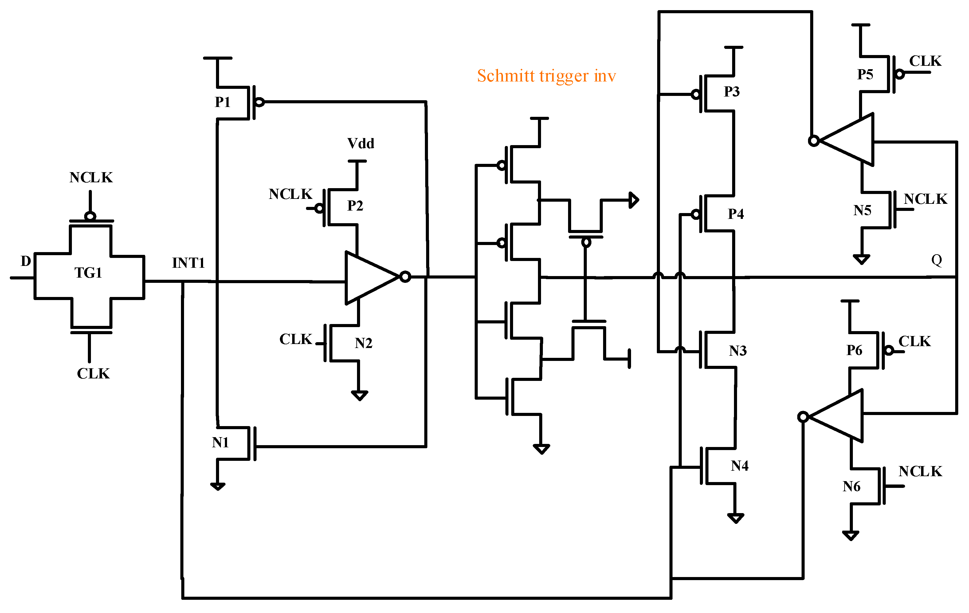
The Schmitt trigger (ST) based latch proposed in [8] is of category 1 as discussed in Section 1. As shown in Figure 1, the latch is focused on the ST hysteresis property and the SET tolerance temporal redundancy. The latch is more reliable than a conventional latch, but it is not completely SEU immune, as stated in category 1. The ST based latch in [8] may upset if a transient fault occurs on an INT1 node.
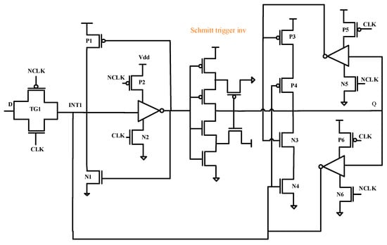
Figure 1.
Schmitt Trigger [ST] based latch in [8].
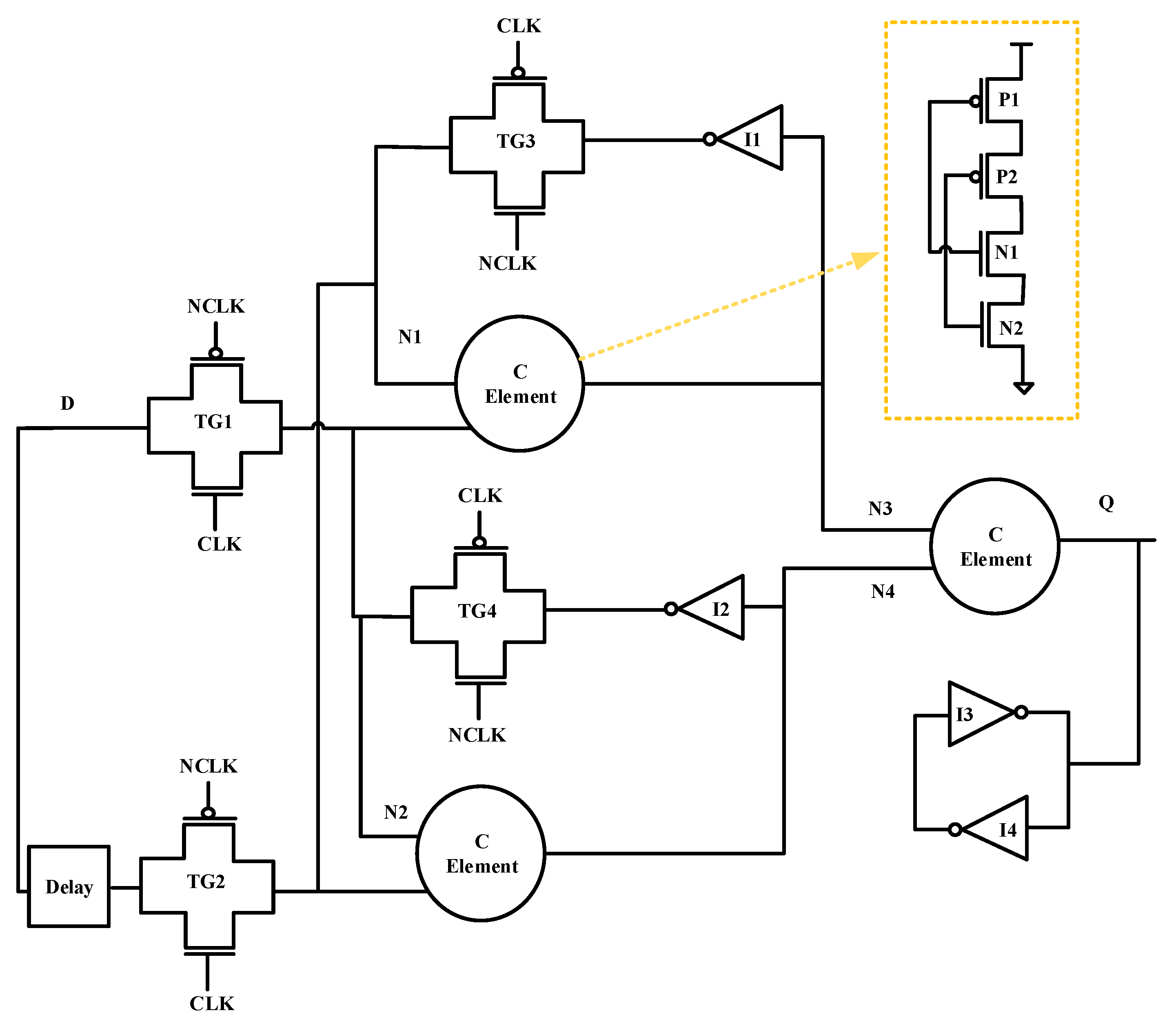
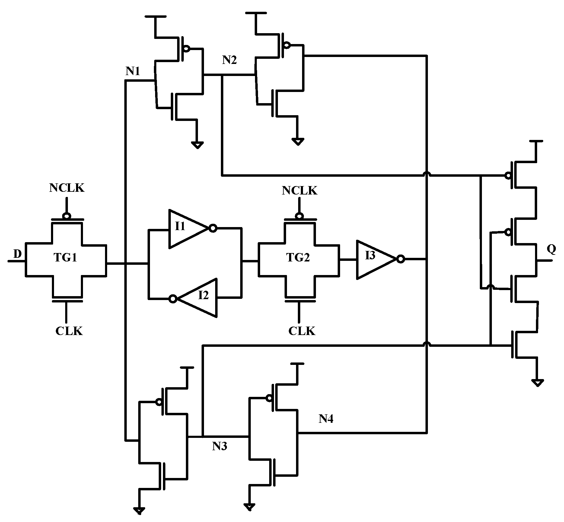
The dual-modular redundancy based SEU tolerant NAN2 latch in [9] is of category 2, as shown in Figure 2 to resolve the issues listed in category 1. The latch in [9] can ensure that no particle hit is impacted, although it does not have input SET filtering capability. The feedback redundant SEU/SET tolerant (FERST) latch shown in Figure 3 comes under category 3 latches. This SEU tolerant FERST latch is focused same as is the latch in [9] on dual- modular redundancy and its significant variations include the construction of dual-modular redundant feedback loops. Also, on the output node Q there is a week keeper circuit. The latch is therefore, insensitive to HISO. Because of the weak keeper, this scheme is not economically efficient. A feedback loop in the weak keeper leads to more power dissipation and delay even in the transparent mode. The HLRCG1 latch in [11] also comes under category 3. However, in the transparent mode, it has a potential current competition on output and internal node of DICE structure. Because of this, there is greater power dissipation in the latch.
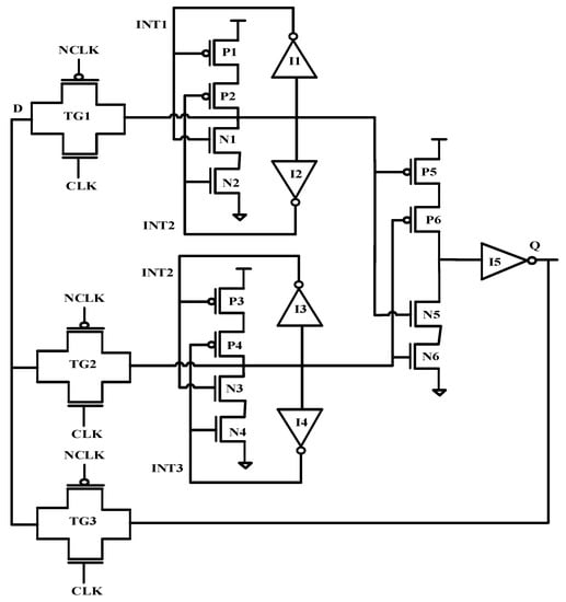
Figure 2.
NAN2 latch in [9].
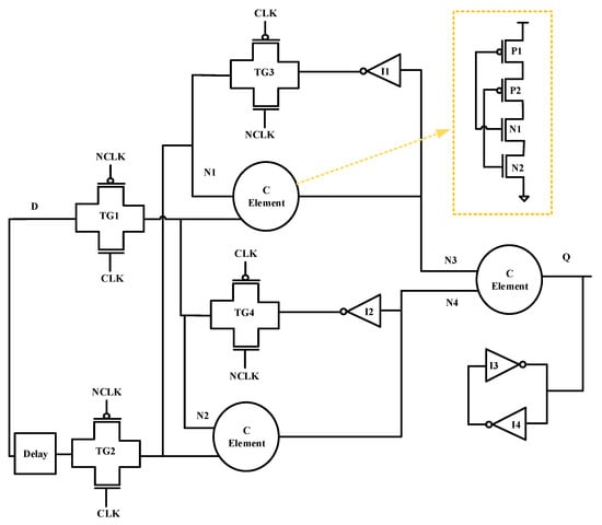
Figure 3.
EVFERST latch in [10].
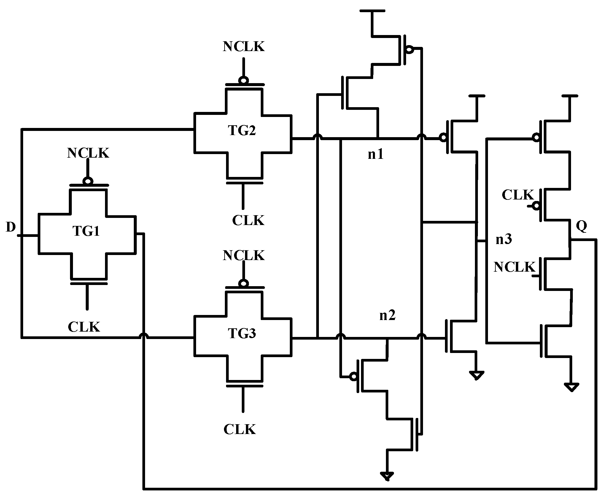
The enhanced version of FERST (EVFERST) in [10], low-cost soft error hardened (LSEH) latches in [12], and SEU resilient and SET filterable latch referred as RFEL latch in [13] are classified as category 4. These latches are more reliable and allow any particle strike to be tolerated. The latches are able to filter out SET since they don’t take a high impedance state at the output node. Nevertheless, these latches occupy a greater area and dissipate more power. Figure 4, Figure 5 and Figure 6 present the LSEH-1, LSEH-2, and RFEL latches, respectively. The energy-efficient SEU tolerant (EEST) latch proposed in [14] is also classified as category 4. The EEST latch shown in Figure 7 includes a clocked Muller C-element and memory element based restorer circuit. This clocked C-element reduces the propagation delay and power dissipation of the circuit by cutting off all the unwanted switching activity. In fact, the efficiency and area consumed by this design is better than the latches mentioned above. But, the main disadvantage of the EEST latch is that it cannot tolerate a positive upset pulse due to a particle hit at node n3. This disadvantage makes the EEST latch less attractive when compared to all the other latches of category 4. The comparison results are presented in Table 2. Furthermore, the issue of active feedback loops in all the above described latches other than EEST latch is certainly present when working in transparent mode. This enhances the power consumption. The proposed latch presented in Section 3 resolves these issues.
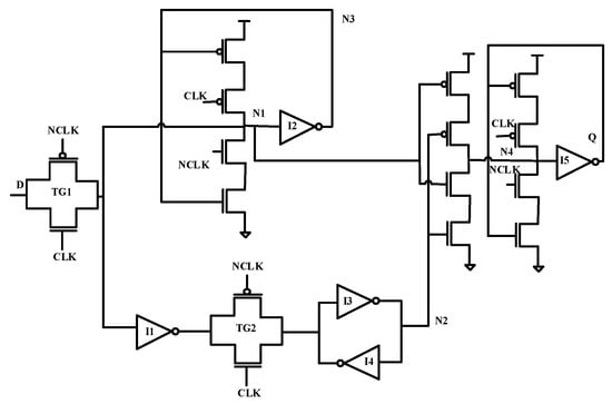
Figure 4.
LSEH-1 Latch in [12].
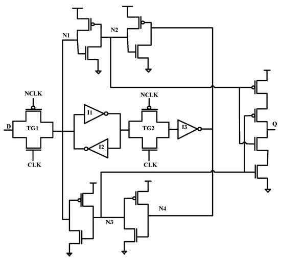
Figure 5.
LSEH-2 Latch in [12].
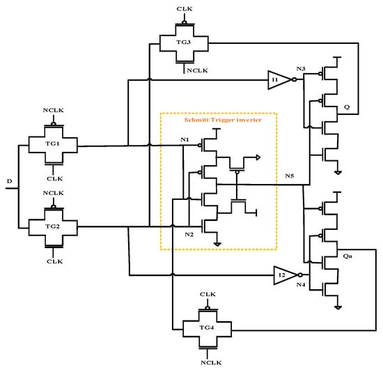
Figure 6.
RFEL latch in [13].
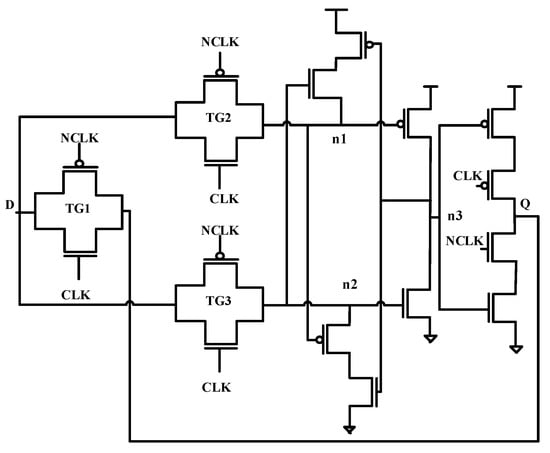
Figure 7.
EEST latch in [14].
3. Proposed LPHS hardened Latch
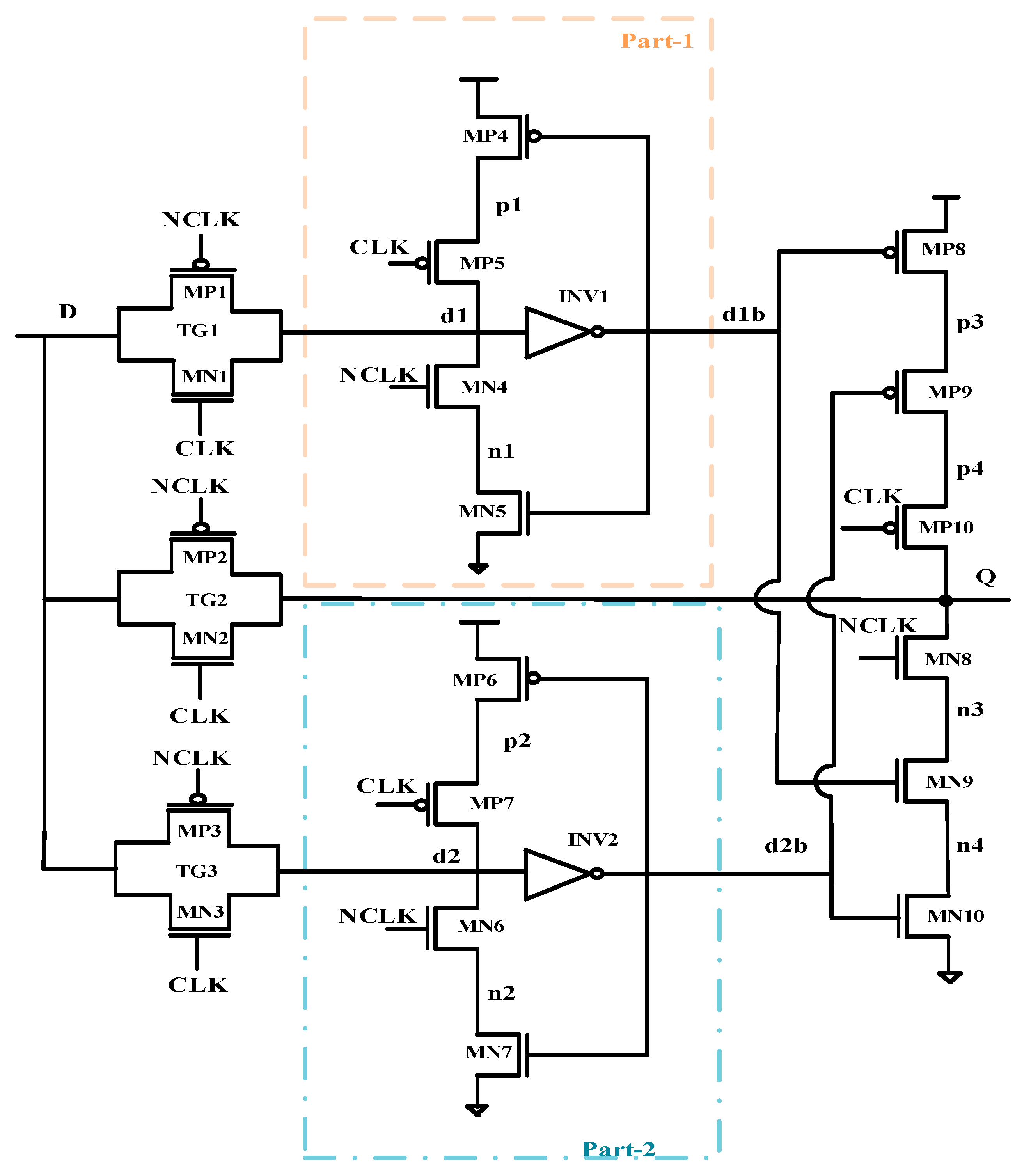
The proposed low power and high speed (LPHS) soft error hardened latch circuit is shown in Figure 8. In the circuit, the data input D is separated into three nodes and connected to three transmission gates (TG1, TG2 and TG3).
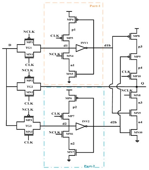
Figure 8.
Proposed LPHS latch.
During the transparent mode (when CLK = 1 and NCLK = 0), the transmission gates TG1, TG2 and TG3 turn on. This enables the data input D to propagate to Q via TG2. The inverters INV1, INV2, feedback loops and Muller C-element are cut off by the clock signal to avoid the contention on Q. During latch mode (when CLK = 0 and NCLK = 1), three transmission gates will be turned off. The feedback loops and the C-element turn on. The path from TG2 to Q deactivates. The two keepers of part-1 and part-2 (termed as intermediate stage) hold the latched values. Through the inverters INV1 and INV2 the data are propagating to C-element and maintains the correct logic at the output node Q.
Now, the detailed analysis of LPHS latch in the presence of transient fault (TF) at various internal nodes in latch mode is explained. Consider D = 1, in the latch mode the internal nodes d1 and d1b of part-1 are 1 and 0 respectively. Likewise, d2 and d2b of part-2 also contain 1 and 0 correspondingly. These d1b and d2b values turn on the PMOS transistors of C-element. In result, the output Q becomes 1. For the above case:
- TF on node d1 (or d1b): if the transient fault occurs at d1 (or d1b), d1 flips its state from 1 to 0, similarly, d1b from 0 to 1. Consequently, part-1 latches the erroneous value, due to the positive feedback structure. Yet, the upset value cannot propagate to the C-element, since part-2 of the latch holds the correct value and leaves the output Q in a high impedance state. Hence, the output is preserved.
- TF on node d2 (or d2b): d2 flips from 1 to 0 and d2b from 0 to 1. Consequently, part-2 latches erroneous value due to the positive feedback loop. Even though, Q will not be impacted, because of the correct values produced by part-1. For data input D = 0, the same operation continues.
If the transient fault occurs on any one of these nodes (p1, n1, p2 and n2), a glitch may be produced at d1 and d2, but this is similar to a transient fault occurring at d1 and d2 as discussed above. If the transient fault occurs at any one of these internal nodes (p3, p4, n3, n4 and Q) mentioned. The output produces a glitch. The produced glitch width and amplitude is directly proportional to the time and amount of charge injected at the node or load capacitance or MP10, MN8 and MP2-MN2 transistor sizes. The output Q will be restored in the absence of particle strike.
3.1. SEU Resilience Verification
In Figure 9, a transient fault is injected at nodes d1 and d2 individually at different time periods for different data inputs. From Figure 9, it can be observed that, at 13ns time period energy particle hits on the node d1, resulting in upset on node d1b. Nevertheless, Q cannot be suffered as node d2b is in its original state. Similarly, from the same Figure 9, it may be noted that if SEU occurs on node d2 at 22 ns, resulting in node d2b upset, but still the correct logic is preserved because of the node d1b. Similar analysis is done for D = 0 and it is true for this case too. Hence, we can conclude that any single event particle strike on nodes d1 (or d1b), d2 (or d2b) cannot upset Q.
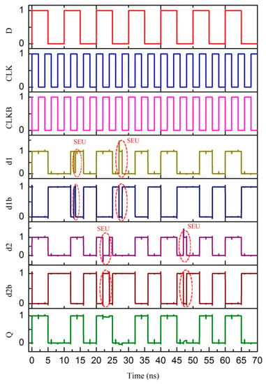
Figure 9.
Injecting SEU on nodes d1, d2 for D = 0 & 1.
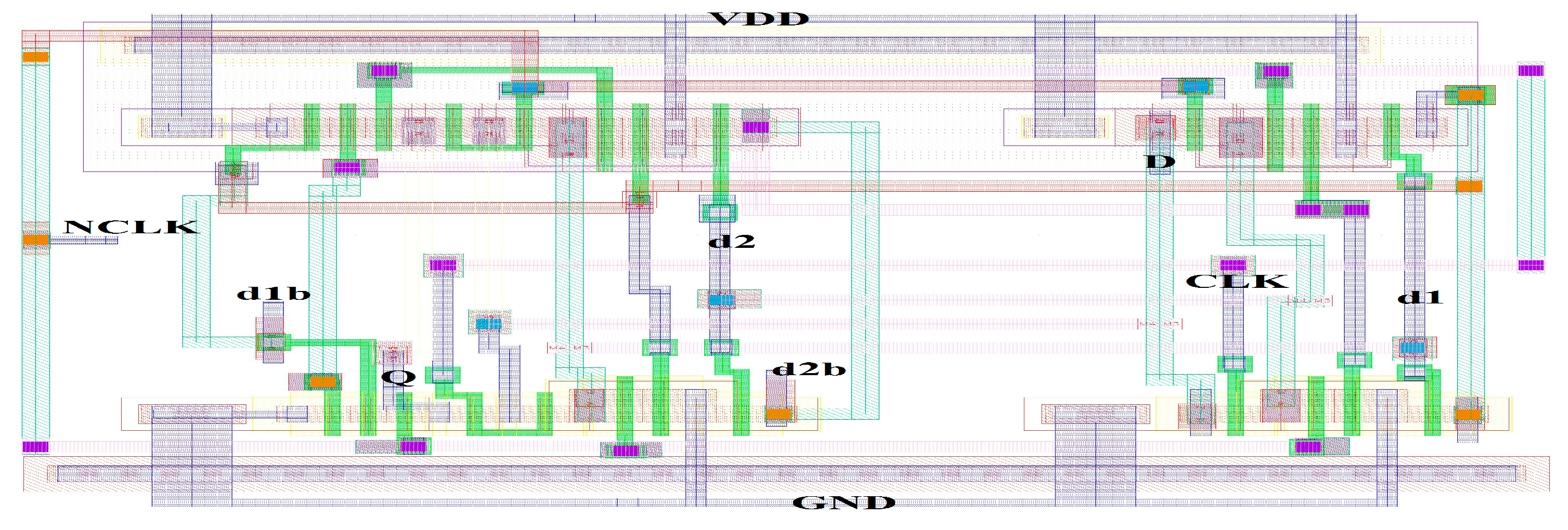
Figure 10 shows the TF occurrence at output node Q. The TF caused by radiation particle strike at output node Q produces a glitch and remains until the effect presents at the node. Nodes d1 and d2 preserve their actual states, implies that the particle hit on Q can only influence Q by placing a wrong value on it. Figure 11 displays the layout of the LPHS latch.
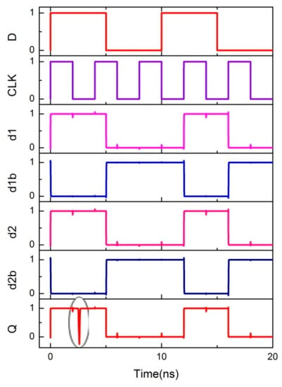
Figure 10.
Transient fault at output node Q.
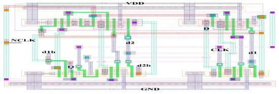
Figure 11.
Layout of the LPHS latch.
3.2. Latch Assessment and Comparison
For the purpose of comparison, the proposed LPHS latch and the latches existing in the literature namely LSEH-1 [12], LSEH-2 [12], NAN2 [9], EVFERST [10], RFEL [13] and EEST [14] are designed using 45 nm CMOS technology [20] with 1 V supply, 250 MHz clock, i.e., clock period of 4 ns and 50% duty cycle at room temperature (27 °C). In this paper the RFEL latch [13] is considered as a reference latch. All these design simulations are carried out using a cadence spectre environment.
Considering the difference in the mobility of PMOS and NMOS devices, the minimum area design rule is adopted for designing the proposed and existing latches. The minimum gate Width/Length (W/L) of PMOS and NMOS are found to be (0.15 μm/0.045 μm) and (0.12 μm/0.045 μm) respectively. The transistor sizing of the proposed LPHS latch is presented in Table 1. The inverters INV1 and INV2 are unit sized inverters.

Table 1.
Transistor sizing of the LPHS latch.
For TF injection, a double exponential current source with the current value as 80μA is used [21]. A time-varying double exponential current equation shown in (1) is used to model the behaviour of particle strike. The equation in (1) may not fully designate all the physics and transient characteristics, though it is used for comparative studies.
In the above Equation (1), I (t) denotes transient current pulse; where Tα denotes collection time constant; Tβ denotes ion track establishment constant and Q = Total deposited charge. Though Tα, Tβ are technology dependent parameters, in [19,22,23,24] with different technology, considered the same values of Tα and Tβ i.e., 0.164 ns and 0.05 ns respectively. For our proposed design the same values are chosen. In order to examine the performance of LPHS latch, its area, delay, power and power delay product (PDP) are calculated. These results are compared with the latches reported in the literature and the same is shown in Table 2. In general, the total power consumption consists of two components, static and dynamic power consumption. Dynamic power is the significant component of power consumption. Switching activity, supply voltage, node capacitance and the feedback loop is a primary factor in dynamic power consumption. The LSEH-1, LSEH-2 and NAN2 latches have more switching activity in transparent mode, allowing them to alter the value saved on node capacitance for longer time. LPHS latch has solved these issues by adding a clock gating circuit to decrease the switching activity and by cutting off all unwanted feedback loops. Consequently, the power consumption of the LPHS latch improves by 84.09%, 85.48%, and 83.45% compared to LSEH-1, LSEH-2, and NAN2 latches, respectively. Similarly, the feedback loop and the weak keeper of EVFERST latch leads to exhibit 62.5% more power dissipation as compared to the LPHS latch. Though, the RFEL latch do not have the active feedback loop in transparent mode, it has slightly increased power, i.e., 8.2% more than the LPHS latch, due to a greater number of transistors used in the circuit configuration. The active feedback loops in transparent mode and a week keeper circuit at the output also increase the propagation delay. The propagation delay of the LPHS latch is reduced by 95.9% 98.8%, 30%, 98.3%, and 94.7% as compared to LSEH-1, LSEH-2, NAN2, EVFERST, and RFEL latch, respectively. From Table 2, it can be observed that the EEST latch shows better performance than the other latches including the proposed LPHS latch. However, the EEST latch shown in Figure 7 is not completely immune to SEU if a positive upset pulse due to particle hit at node n3 occurs.

Table 2.
Performance comparison.
4. Supply Voltage, Temperature and Process Variation Effects
This section addresses the effects of process, supply voltage, and temperature variations (PVT) on the LPHS latch. Monte-Carlo (MC) simulations has been carried out for 500 runs using Cadence Spectre and presented the results in Table 3. The power and delay of LPHS latch is simulated under various process corners such as typical (tt), fast (ff) and slow (ss) for varied supply voltages (±10% of VDD), and the temperature ranges from 0 °C to 100 °C [25]. From Table 3, it can be observed that the power consumption increases with the increase in supply voltage because high supply voltages offer high noise margins [26]. Consequently, the noise level to influence the circuit increases. Nevertheless, the D to Q delay decreases due to increase in the supply voltage, because high supply voltages influence high currents into the device. Table 2 also shows the deviation in power consumption and delay for various temperatures.

Table 3.
Power and Delay of LPHS latch under PVT variations.
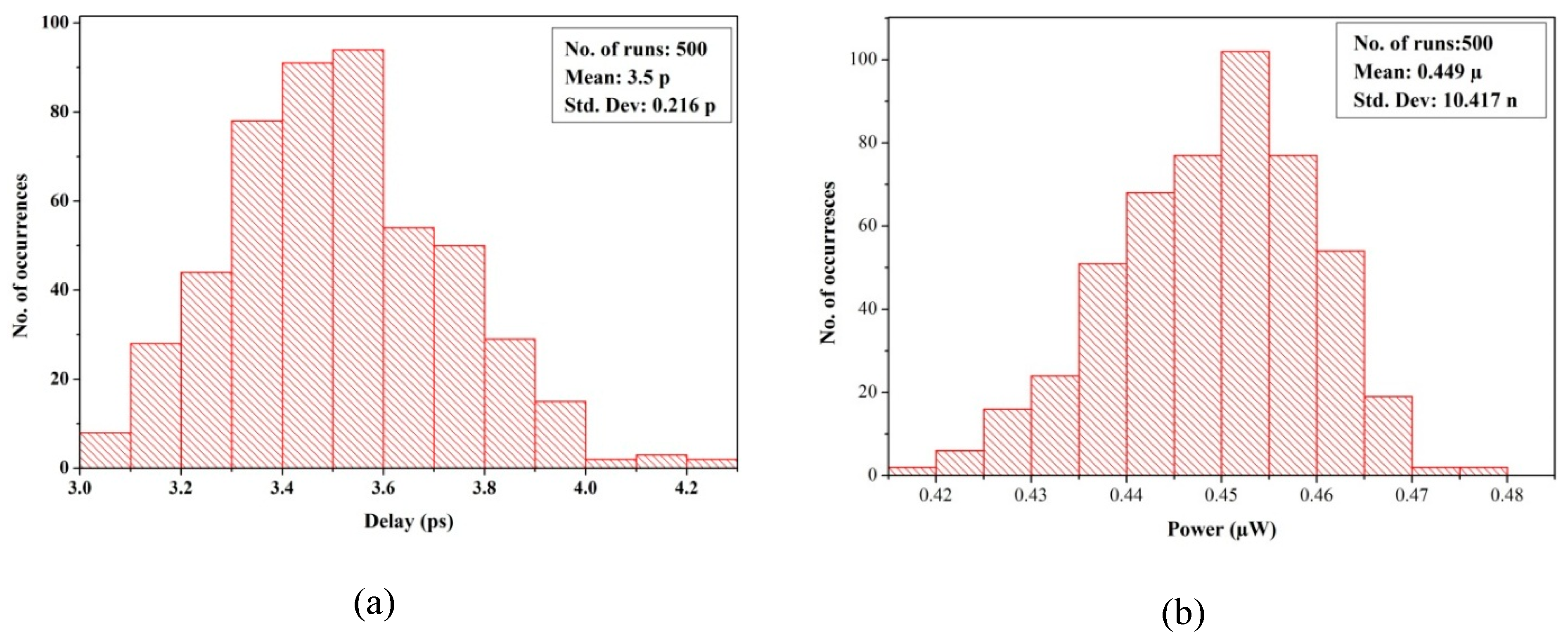
Figure 12 displays the impact of PVT variations on D to Q delay and the power consumption of the LPHS latch for typical corners. From Figure 12, it can be noted that the mean value of delay and power consumption of LPHS latch are 3.5 ps and 449 nW respectively, which are almost equal to the simulated values. MC simulations of the LPHS latch show that the distributions of delay and power consumption differ with a standard deviation of only 3.6% and 2.3%, respectively.
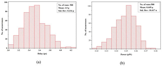
Figure 12.
Monte Carlo Simulations of LPHS latch (a) Delay (b) power.
5. Conclusions
To conclude, this paper proposes a low power and high speed (LPHS) SEU hardened latch design which is implemented in CMOS 45 nm technology. In the proposed LPHS latch, a reduction in delay and power is achieved by adopting four feedback loops in the intermediate stage and the clock gating technique. These techniques help in reducing unwanted switching activity in the transparent mode, thereby reducing the delay and power dissipation. Subsequently, the dual input Muller C-element prevents the propagation of SEU to the output node. Simulation results confirm that the LPHS latch is capable of tolerating SEU on any of the internal nodes of the intermediate stage. The comparison results also show that the LPHS latch exhibits a reduction in power consumption, delay, and PDP by 8%, 95%, and 94%, respectively, as compared to the existing single event upset resilient and single event tolerant latches. Monte Carlo results shows that the proposed latch is less sensitive to the process, supply voltage, and temperature variations.
Author Contributions
Methodology, S.K.S.; Supervision, K.S.
Funding
This research received no external funding.
Conflicts of Interest
The authors declare no conflict of interest.
References
- Dodd, P.E.; Massengill, L.W. Basic mechanisms and modeling of single-event upset in digital microelectronics. IEEE Trans. Nucl. Sci. 2003, 50, 583–602. [Google Scholar] [CrossRef]
- Ferlet-Cavrois, V.; Massengill, L.W.; Gouker, P. Single event transients in digital CMOS—A review. IEEE Trans. Nucl. Sci. 2013, 3, 1767–1790. [Google Scholar] [CrossRef]
- Markovic, D.; Wang, C.C.; Alarcon, L.P.; Liu, T.T.; Rabaey, J.M. Ultralow-power design in near-threshold region. Proc. IEEE 2010, 2, 237–252. [Google Scholar] [CrossRef]
- Nicolaidis, M. Design for soft error mitigation. IEEE Trans. Device Mater. Reliab. 2005, 3, 405–418. [Google Scholar] [CrossRef]
- Liu, P.; Zhao, T.; Liang, F.; Zhao, J.; Jiang, P. A power-delay-product efficient and SEU-tolerant latch design. IEICE Electron. Express 2017, 23, 20170972. [Google Scholar] [CrossRef][Green Version]
- Xu, H.; Zhu, J.; Lu, X.; Li, J. An advanced SEU tolerant latch based on error detection. J. Semicond. 2018, 5, 055003. [Google Scholar] [CrossRef]
- Toro, D.G.; Arzel, M.; Seguin, F.; Jézéquel, M. Soft error detection and correction technique for radiation hardening based on C-element and BICS. IEEE Trans. Circuits Syst. II: Express Briefs 2014, 12, 952–956. [Google Scholar] [CrossRef]
- Shirinzadeh, S.; Rahebeh, N.A. A novel soft error hardened latch design in 90nm CMOS. In Proceedings of the 16th CSI International Symposium on Computer Architecture and Digital Systems (CADS 2012), Shiraz, Iran, 2–3 May 2012; pp. 60–63. [Google Scholar]
- Nan, H.; Ken, C. Low cost and highly reliable hardened latch design for nanoscale CMOS technology. Microelectron. Reliab. 2012, 6, 1209–1214. [Google Scholar] [CrossRef]
- Fazeli, M.; Miremadi, S.G.; Ejlali, A.; Patooghy, A. Low energy single event upset/single event transient-tolerant latch for deep subMicron technologies. IET Comput. Digit. Tech. 2009, 3, 289–303. [Google Scholar] [CrossRef]
- Nan, H.; Ken, C. High performance, low cost, and robust soft error tolerant latch designs for nanoscale CMOS technology. IEEE Trans. Circuits Syst. I Regul. Pap. 2012, 7, 1445–1457. [Google Scholar] [CrossRef]
- Rajaei, R.; Mahmoud, T.; Mahdi, F. Low cost soft error hardened latch designs for nano-scale CMOS technology in presence of process variation. Microelectron. Reliab. 2013, 6, 912–924. [Google Scholar] [CrossRef]
- Yan, A.; Liang, H.; Huang, Z.; Jiang, C.; Ouyang, Y.; Li, X. An SEU resilient, SET filterable and cost effective latch in presence of PVT variations. Microelectron. Reliab. 2016, 63, 239–250. [Google Scholar] [CrossRef]
- Kumar, C.I.; Anand, B. High performance energy efficient radiation hardened latch for low voltage applications. Integration 2019, 66, 119–127. [Google Scholar] [CrossRef]
- Nan, H.; Ken, C. Novel radiation hardened latch design considering process, voltage and temperature variations for nanoscale CMOS technology. Microelectron. Reliab. 2011, 12, 2086–2092. [Google Scholar] [CrossRef]
- Yan, A.; Liang, H.; Huang, Z.; Jiang, C.; Yi, M. A self-recoverable, frequency-aware and cost-effective robust latch design for nanoscale CMOS technology. IEICE Trans. Electron. 2015, 12, 1171–1178. [Google Scholar] [CrossRef]
- Liang, H.; Wang, Z.; Huang, Z.; Yan, A. Design of a radiation hardened latch for low-power circuits. In Proceedings of the 2014 IEEE 23rd Asian Test Symposium, Hangzhou, China, 16–19 November 2014; pp. 19–24. [Google Scholar]
- Wang, H.; Dai, X.; Wang, Y.; Nofal, I.; Cai, L.; Shen, Z.; Sun, W.; Bi, J.; Li, B.; Guo, G.; et al. A single event upset tolerant latch design. Microelectron. Reliab. 2018, 88, 909–913. [Google Scholar] [CrossRef]
- She, X.; Li, N.; Tong, J. SEU tolerant latch based on error detection. IEEE Trans. Nucl. Sci. 2012, 1, 211–214. [Google Scholar] [CrossRef]
- Zhao, W.; Yu, C. New generation of predictive technology model for sub-45 nm early design exploration. IEEE Trans. Electron. Devices 2006, 53, 2816–2823. [Google Scholar] [CrossRef]
- Munteanu, D.; Autran, J.L. Modeling and simulation of single-event effects in digital devices and ICs. IEEE Trans. Nucl. Sci. 2008, 4, 1854–1878. [Google Scholar] [CrossRef]
- Messenger, G.C. Collection of charge on junction nodes from ion tracks. IEEE Trans. Nucl. Sci. 1982, 6, 2024–2031. [Google Scholar] [CrossRef]
- Xuan, S.X.; Li, N.; Erstad, D.O. SET tolerant dynamic logic. IEEE Trans. Nucl. Sci. 2012, 59, 434–438. [Google Scholar]
- Lu, Y.; Lombardi, F.; Pontarelli, S.; Ottavi, M. Design and analysis of single-event tolerant slave latches for enhanced scan delay testing. IEEE Trans. Device Mater. Reliab. 2014, 141, 333–343. [Google Scholar]
- Weste, N.H.; Harris, D. CMOS VLSI Design: A Circuits and Systems Perspective; Pearson Education India: Noida, India, 2015. [Google Scholar]
- Wakerly, J.F. Digital Design: Principles and Practices; Pearson Education Australia: Melbourne, Australia, 2001. [Google Scholar]
© 2019 by the authors. Licensee MDPI, Basel, Switzerland. This article is an open access article distributed under the terms and conditions of the Creative Commons Attribution (CC BY) license (http://creativecommons.org/licenses/by/4.0/).

