Article

Starting Framework for Analog Numerical Analysis for Energy-Efficient Computing

Electrical and Computer Engineering (ECE), Georgia Institute of Technology, Atlanta, GA 30332-250, USA
J. Low Power Electron. Appl. 2017, 7(3), 17; https://doi.org/10.3390/jlpea7030017
Submission received: 24 April 2017 / Revised: 20 June 2017 / Accepted: 20 June 2017 / Published: 27 June 2017
(This article belongs to the Special Issue Design Methodologies for Power Reduction in Consumer Electronics)

Abstract

:
The focus of this work is to develop a starting framework for analog numerical analysis and related algorithm questions. Digital computation is enabled by a framework developed over the last 80 years. Having an analog framework enables wider capability while giving the designer tools to make reasonable choices. Analog numerical analysis concerns computation on physical structures utilizing the real-valued representations of that physical system. This work starts the conversation of analog numerical analysis, including exploring the relevancy and need for this framework. A complexity framework based on computational strengths and weaknesses builds from addressing analog and digital numerical precision, as well as addresses analog and digital error propagation due to computation. The complimentary analog and digital computational techniques enable wider computational capabilities.

1. Introduction

The range of digital and recent analog computation (e.g., [1]) leaves the system application designer wondering what approach to utilize for different computational pieces. Figure 1 shows the designer’s dilemma choosing analog or digital computing platforms. Digital computation is enabled by a framework developed over the last 80 years. Most system designers will choose digital computation over analog computation explicitly or implicitly because a digital framework exists, and the core of their STEM education, even when it results in drastically lower performance. Hardware-software co-design, almost entirely digital co-design between processors and FPGAs, is a currently researched discipline (e.g., [2,3,4,5,6,7,8]). Having an analog framework enables wider capability while giving the designer tools to make reasonable choices.
The focus of this work is to develop a starting framework for analog numerical analysis and related algorithm questions. My working definition of numerical analysis is the mathematical and algorithmic computational framework including the tradeoff of algorithms, numerical representations and resulting error propagation (e.g., Signal-to-Noise Ratio (SNR)), in a particular physical computing structure. All computation occurs in physical devices, even though the representation may be abstract or idealized. The particular physical structure used for computation influences the choice of particular computational algorithms. Digital numerical analysis concerns computation on synchronous digital hardware. Analog numerical analysis concerns computation on physical structures utilizing the real-valued representations of that physical system.
We see this work as starting the conversation of analog numerical analysis. This discussion will build a starting foundation for analog numerical analysis over the next several sections. These sections will address both digital and analog considerations and their comparisons, as appropriate. The first section explores the relevancy and need for analog numerical analysis, in particular, given the demonstration of analog computation. The second section addresses analog and digital numerical precision, the strength of digital numerical techniques. The third section addresses analog and digital error propagation due to computation, an apparent strength of analog numerical techniques. The fourth section then builds a complexity framework based on computational strengths and weaknesses. The complimentary analog and digital computational techniques enable wider computational capabilities. This paper presents a first-discussion on analog numerical analysis, a key first step towards starting a unified physical-computing framework.

2. Why Analog Numerical Analysis?

Initially, one might wonder: Why consider analog computation at all? Although energy efficiency in digital computation improved dramatically with scaling down of transistors, the issue of threshold voltage ( V T 0 ) mismatch between transistors has effectively brought energy efficiency of commercial digital ICs to a standstill [9,10]. This digital processing energy efficiency wall calls out for new solutions to meet the appetite of the next generation of computing.
In 1990, Carver Mead hypothesized that custom analog solutions could have at least a 1000× improvement over custom digital solutions [11]. This hypothesis gives hope that new computing structures might be possible. A factor of 1000 improvement in energy efficiency is roughly equivalent to the improvement from the start of DSP (1978) [12] to the digital energy efficiency wall of 10 MMAC (/s)/mW (MMAC = Million Multiply Accumulate). The computational capability of analog computation compared to digital computation (1000×) lower energy/power, 100× lower area) could possibly open the next wave of computing [13].
The following sections consider digital and analog computation, in turn.

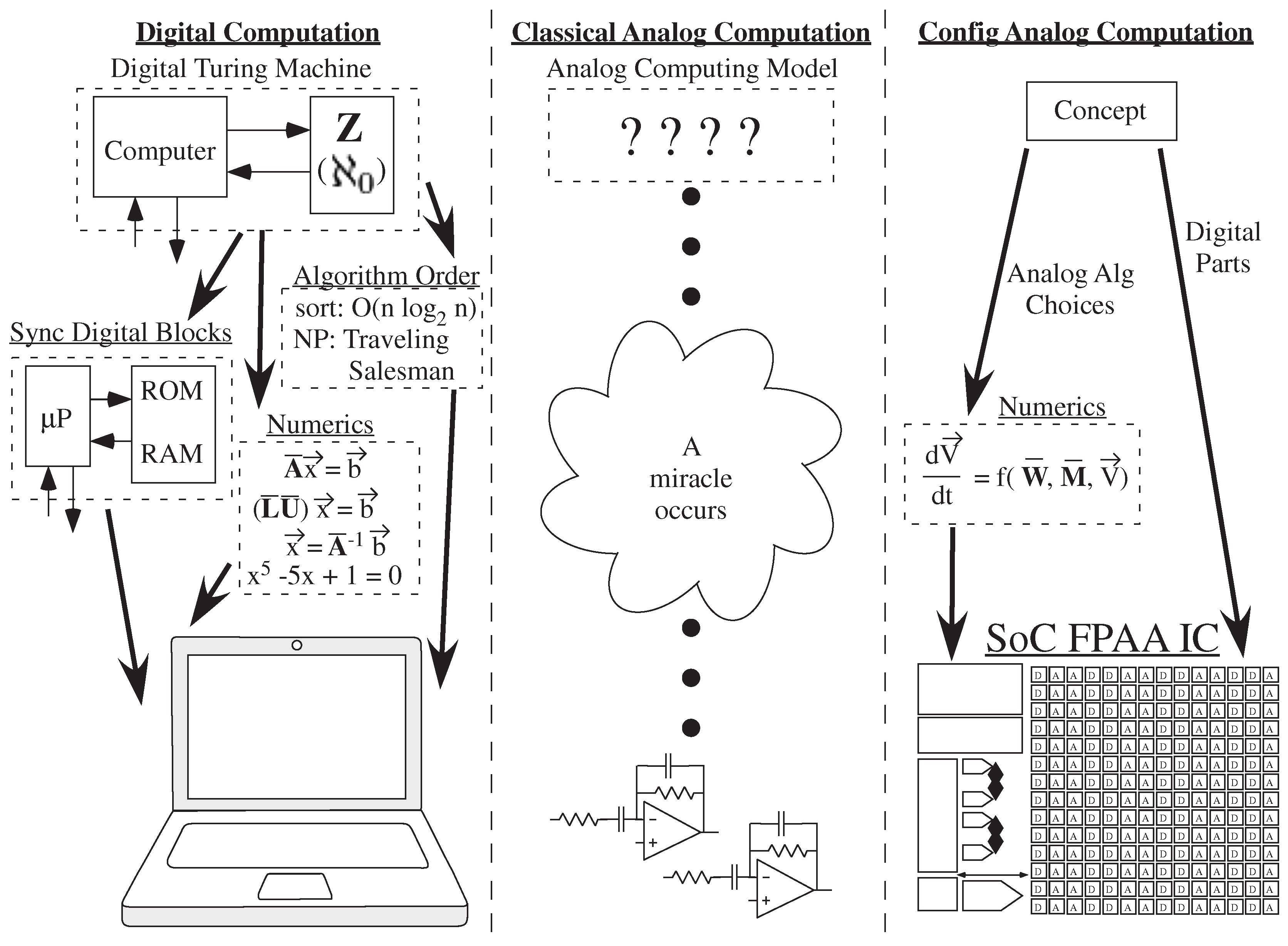
2.1. Digital Framework Enables Ubiquitous Numerical Computation

Numerical analysis for digital computing seems like an established discipline [14,15,16]; coupled with Turing’s original model of computation [17], one has a ubiquitous theory of modern computational devices. When digital computation became more powerful and less expensive in the 1970s and 1980s, digital numerical analysis techniques were already an established and growing discipline. These techniques provided potential computational roadmaps for the exponential computational increase from the digital VLSI revolution [18].
Numerical analysis provides guidance on the algorithmic approaches for numerical algorithms, as well as preferred analytical representations, even if one is unaware of anything explicitly in numerical analysis. Digital computation already had over 30 years of efforts in the numerical and algorithm analysis at the start of the digital VLSI revolution [18]; therefore, the computing framework was rarely in question during the exponential growth of transistors and resulting computational complexity. Digital computation became the dominant computational approach primarily because of its programmability, empowering whole communities to program digital systems for a wide range of applications, (e.g., using microprocessors ( μ P)), that would not ever design any physical system.

2.2. Analog Computing Has Arrived, But Lacks a Framework

Analog numerical analysis was never developed during the classical analog computing time frame. Traditional analog computing was considered by multiple authors (e.g., [19,20]); the solutions were a series of special case solutions with little overarching computational model (Figure 2). Analog computation relied on individual artistic approaches to find the particular solution (Figure 2). MacLennan provides a review of early analog computation [21].
The modern development of analog computation started with almost zero computational framework. Modern analog computation started simultaneously with neuromorphic (including neural network) resolution in the 1980s (e.g., [22,23,24]); these two fields have been tightly linked ever since. The lack of a computational framework gives some understanding why large-scale analog computation has taken so long to be realized since the renewed interest in physical/analog computation. The requirement of a ubiquitous long-term memory and computing element, first introduced in 1994, became essential for practical analog computation [25]. Without configurable and programmable systems, analog computing discussions are mostly of a theoretical nature. Further, the success of programmable digital approaches nearly pushed out generations of students being familiar with analog computation, as well as basic analog circuit design.
Many memory devices and circuits are used for analog memories. State variables provide short-term memory of previous events. A first-order low-pass filter (e.g., capacitor and resistive element) has memory of past events (e.g., [24]), efficiently using typically-occurring state variables as part of the computation rather than fighting against these devices. These techniques are typically limited to the order of 1-s timescales. Floating-Gate (FG) devices and circuits (e.g., [25]) have provided long-term memories for analog computation, enabling very precise programming of values (e.g., 14 bit [26]) for long-term lifetimes (e.g., [27,28]). Memory elements on the order of minutes or longer tend to be more challenging, but possible using adaptive FG techniques from ms to years [29,30], at reasonably low power, including in configurable spaces [31]. Another potential option will be using other long-time-dependent devices, like memristors [32], demonstrated to be integrated with this form of computation. Sometimes long-delay lines are required for a particular operation (e.g., linear-phase filters). These can be achieved by cascades of delay stages (e.g., ladder filter [33]), as well as distributed analog arithmetic [34] that uses digital intermediate representations for delay stages. Other sampled memory approaches are used when the incoming data are already sampled, with a variety of additional techniques possible (e.g., [35]). The most efficient physical computation is one operating at the speed of the incoming data (and/or speed of output data) to minimize the amount of memory storage. This type of memory storage always adds additional complexity, costs a significant amount of power for an analog computation and typically adds cost to digital computation, as well.
Programmable and configurable ultra-low power computation due to physical (e.g., analog) computing is becoming a reality. The capability of programmable and configurable analog/mixed mode computation, large-scale Field Programmable Analog Arrays (FPAA) (e.g., [1]), enables ubiquitous use of this technology similar to the use of microprocessors and related programmable digital hardware (Figure 3). The SoC FPAA configurable fabric uses inter-digitized analog and digital computation blocks, blurring the boundary between these two domains. Data-converters or their more general concepts, analog classifiers, typically have digital outputs and require digital control. Most analog computation will require both analog and digital parts.
Giving a causal look at Figure 3, one notices that Analog (A) CABs (CAB = Computational Analog Block) and Digital (D) CLBs (CLB = Computational Logic Block) columns are interdigitated. One might have expected a bank of analog components and a bank of digital components with data converters (ADCs and DACs) moving between these two regions. Figure 3 does not use this approach. Analog or digital signals can be routed on the same fabric [1] and can be used by CABs or CLBs. Early attempts at these approaches were considered earlier [36,37]. Why would one take this approach? For example, if one needs to compile an ADC, one needs some analog and some digital processing. Where one would put the ADC is not clear and entirely system dependent. Building classifiers have analog inputs and digital outputs. Analog or digital signals could be routed to the processor’s general purpose I/O or to its interrupt lines. Digital symbols are often used to control the analog processing data path. Once one gets beyond artificial boundaries between analog and digital processing, potential opportunities are significant, particularly when high-performance computing (ODEs, PDEs) are done by analog methods.
The design tools (and abstractions) [38,39], infrastructure [40] and FPAA ICs [1] developed have reached a stable point, across multiple IC fabrication processes [41], where they are used in educational [40] and research environments. The open-source design tool framework utilizes a graphical, high-level data flow language and automatically compiles, places, routes and programs the configurable IC, as well as macro-modeled simulation of the system (Figure 4).
It has already been shown that certain functions such as Vector-Matrix Multiplication (VMM), frequency decomposition, adaptive filtering and Winner-Take-All (WTA) are a factor of 1000× more efficient than digital processing (e.g., [1]). Recent demonstrations show sensor processing through embedded classification and machine learning techniques integrating training algorithms [42]. Enabling further biologically-inspired classifier techniques opens the opportunity for configurable biologically-inspired, energy-efficient classifier approaches (factor of 1000 to 1,000,000 over custom digital solutions) [43] for context-aware applications (Figure 3).
One might wonder if fundamental analog building blocks, both in hardware and in the software tools, can be reasonably determined in a similar way one uses look-up tables and flip-flops for FPGA designs? We will summarize the key points here; the detailed discussions are beyond the scope of this paper.
Digital FPGA components did not start off being obvious. The approaches used came from the same individuals who were working on look-up tables and and-or logic components. There was not a methodology, but rather a good approach that, when scaled up, has been effective. Today, these approaches seem sufficient for most tasks, particularly since FPGA architectures are partially hidden from their users.
Analog computation has not had a similar set of blocks because analog computation did not build up a computational framework to enable the transition to these higher levels. The rise of FPAA approaches has become the testbed to begin to build this framework. Comparing the CABs of early papers [44] to the CAB topology of recent FPAA designs (e.g., Figure 2 in [1]) shows some similar characteristics, validated by numerous circuits designed and measured in these architectures. Over a decade of consistent FPAA development and application design has roughly converged on a typical mixture of several medium level components per CAB (Transconductance Amplifiers (OTAs), FG OTAs, T-gates), along with a few low level elements (transistors, FG transistors, capacitors). A few CABs might be specialized for larger functions (e.g., signal-by-signal multipliers [1], sensor interfacing [45], neurons [36]), showing their relative importance in these discussions. Most of these elements have at least one FG parameter that is part of the particular device used. For small to moderate CAB components, the complexity of the resulting device is roughly proportional to the number of pins available for routing. Three terminals of an nFET transistor have similar system complexity to three terminals of an FG OTA. We expect some small shifts in these components in future FPAA devices, such as dedicated current-conveyer blocks, but generally, the CAB level components are stable. Like FPGAs, where the number and size of LUTs vary from architecture to architecture, one expects similar variation for different FPAA devices.
Early recognition of FG switches (e.g., CAB selection crossbars) as computational elements [46] both enabled a wide range of computations (e.g., VMM [47]), as well as brought creative energy to the routing infrastructure (history described in [1]) and resulting novel tool framework. In such architectures, the CAB components become as much the boundary conditions for the computation as the computation itself. Finally, the ability to abstract analog blocks, with digital components, into higher level abstractions enabled by the Scilab/Xcos toolset starts to illuminate the higher-level representations for analog computation.
Analog numerical analysis enables faster system-level designs enabling a roadmap for various applications. The process requires bringing out the lore of a few master research groups to a wider group of designers. The widespread emergence of analog computing hardware (e.g., [48,49] will only accelerate this process.

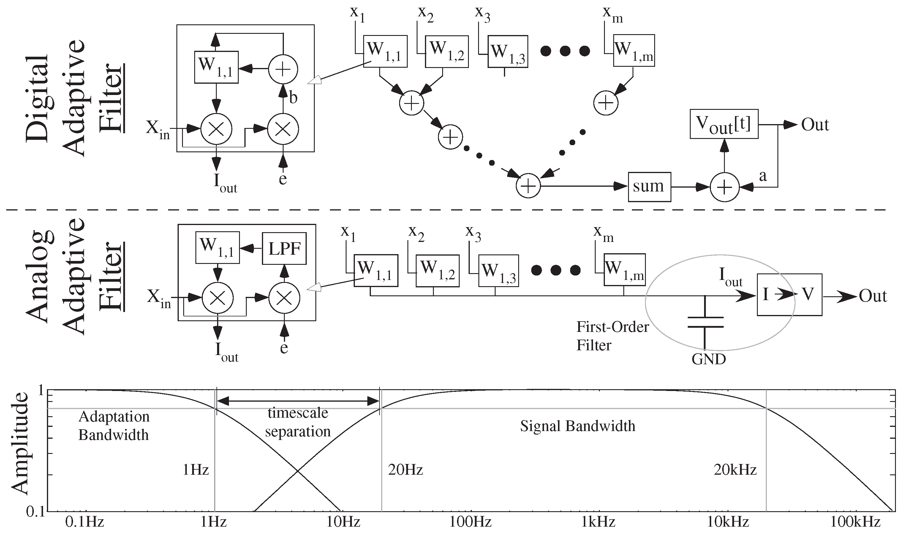
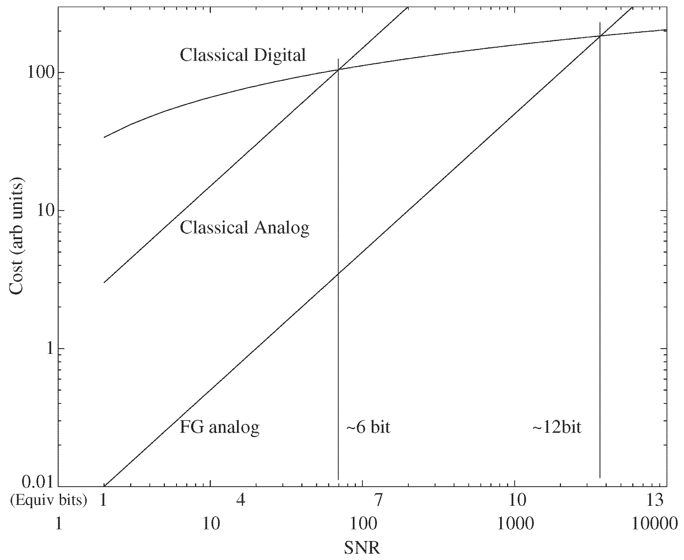
3. Digital Strength: Lower Cost Numerical Precision

After one appreciates the very real and practical possibility of programmable and configurable analog systems, the next questions concern the noisy or low-precision issues real and perceived in analog systems. The issue starts by noting mismatch between typical circuit components, particularly transistors and capacitors, setting the performance of analog computing structures [50]. Analog computation requires many devices, and therefore, accuracy is compounded by the larger number of mismatched devices. For example, one study for real-time acoustic computation shows significant degradation of system performance due to mismatch [51]; although some techniques can be used to improve these models [52,53], without dealing directly with the mismatch, the performance of these systems will always be limited. As IC processes shrink to smaller transistor dimensions (e.g., 40 nm and below) and power supplies, these issues become almost insurmountable for analog design. Digital computation being limited by V T 0 mismatch [9] makes the situation for analog computation look less likely.
Figure 5 shows the precision of storage and simple element SNR versus expected cost, showing that analog has advantages for lower precision and showing digital has advantages for higher precision after a particular crossover point. SNR is defined at the ratio of the largest signal, limited by hard limits or linearity, to the smallest signal, limited by noise. Multiple authors have utilized this framework starting from Hosticka [54], then by Vittoz for simple filters [55], and utilized by others for basic computational blocks [56,57,58,59]. Digital computation has a moderate to low cost for adding additional precision, although it starts with higher starting overhead. Digital cost is effectively proportional to the number of bits = log 2 (precision). As one adds another bit, one increases the apparent precision of that value by a factor of two; doubling a register size significantly increases its precision (e.g., eight bits at 0.4% to 16 bits at 0.0015%). To increase analog precision by one bit requires an increased cost of least a factor of two classically, primarily to deal with component mismatch, as well as current noise [60]. Analog precision cost is a polynomial function of the target SNR.
Analog programmability moves the crossover point, illustrated in Figure 5, to higher SNR levels. The use of Floating-Gate (FG) devices (e.g., [25]) enables directly programming out these issues, including accounting for a range of temperatures (e.g., [28,47]). Calibration of FG devices, particularly in FPAA devices, has been extensively studied and experimentally shown [61,62]. Figure 6 shows the significant opportunities of programmable FG analog concepts compared to alternative approaches, a DAC for every parameter. Before these concepts were possible (e.g., [25]), the analog processing community struggled for any reasonable solution for this approach (e.g., [63]). Neurobiological systems seem to adapt around its mismatches to create precision in its analog computational structures [43]. With programmable systems, resolution is limited by thermal noise [60] and not in component mismatch, resulting in a lower cost for similar precision.
A related issue is that input sensors rarely output SNR greater than 10 to 14 bits, although the dynamic range might be a few orders of magnitude (e.g., a floating-point type representation, whether analog or digital). The resulting analog starting precision for these typically analog sensors matches with the resolution requirements of analog precision. Further, many initial sensor computations require subtraction of similar values (e.g., spatial beamforming), resulting in lower signal SNR independent of the computing approach. This catastrophic cancellation further matches analog computing to the incoming data; higher precision is then primarily useful to offset any numerical computation inaccuracies.

4. Analog Strength: Better Numerical Operations

This section considers the error propagation issues for computation, first for digital computation and then for analog computation. Digital computation aligns well with matrix equation solutions. Analog computation aligns well with the solution of differential equations, both Ordinary Differential Equations (ODE) and Partial Differential Equations (PDE).

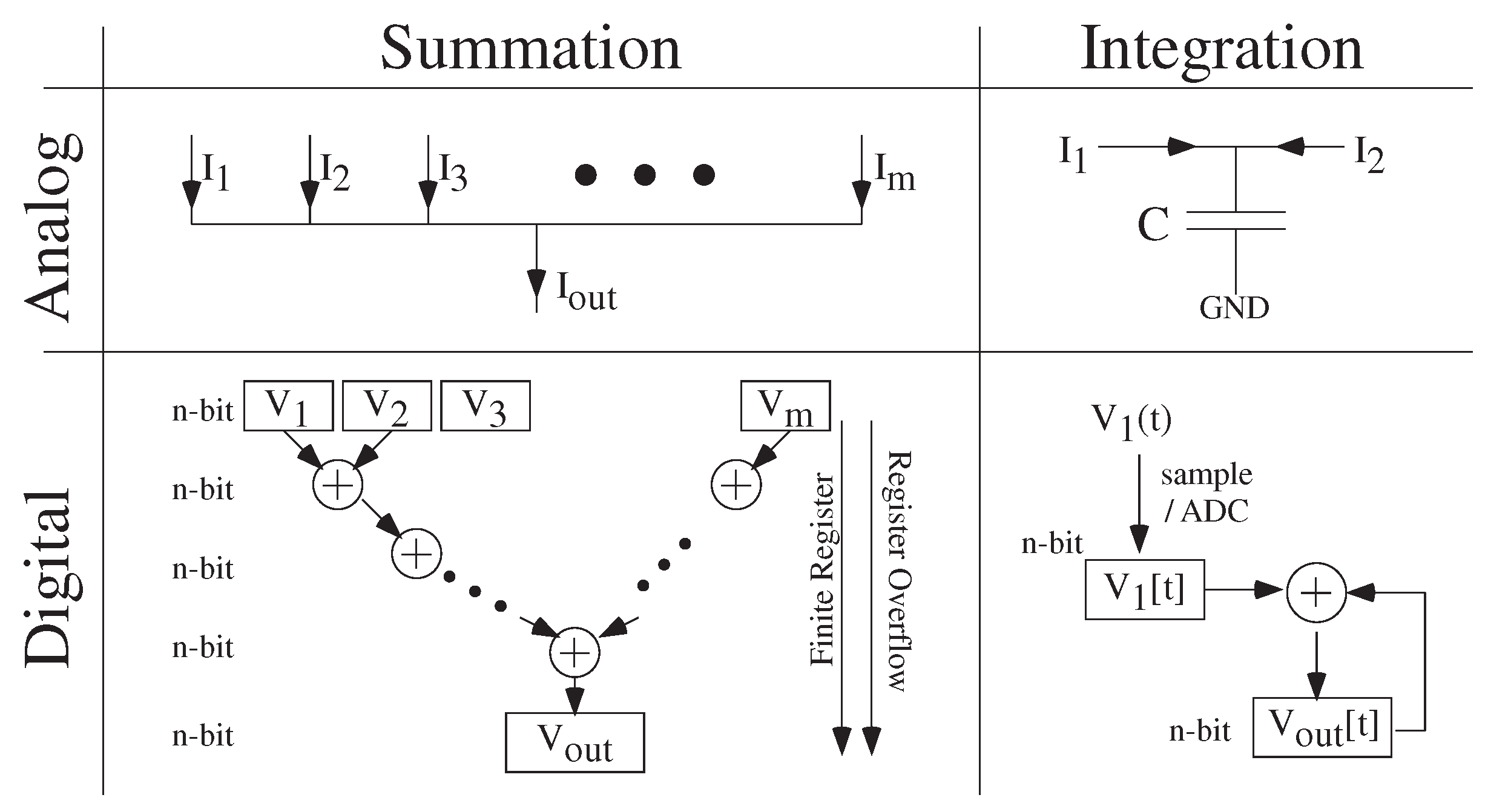
4.1. LU Decomposition as the Basis of Digital Numerics

The question then turns to a question of the apparent low SNR of individual analog computations aggregating into a larger computation. These algorithmic analyses tend to follow digital numerical viewpoints modeling the propagation of digital noise (Figure 7). Digital summation is filled with noise errors. The sum of two n-bit numbers half the time will be an n + 1 bit number. As the average case, we potentially get 1 2 log 2 m due to the finite register, and potentially, we get 1 2 log 2 m due to register overflow. One either handles fixed-point arithmetic issues by having large enough total resolution for the summation to avoid overflow nonlinearities or handles floating-point arithmetic issues by having enough mantissa bits to account for the Least Significant Bit (LSB) noise source. The issue for digital computation is a large number of aggregate summations; 1024 summations will lose five bits of precision on average and 10 bits in the worst case. For 16-bit registers, this error can be significant; we have not addressed any further errors due to catastrophic subtraction of similar numbers. Integration, often implemented as a sequence of summations, further compounds these numerical issues. Further, integration must be approximated by a set of small regions. Too few steps, and one gets low accuracy. Too many steps, and the summation errors result in low accuracy. The ODE solution further complicates these issues with numerical stability issues (Figure 7), order of derivative approximations, as well as stiff ODE computations.
An engineer faced with these issues most naturally would try to reformulate a problem (ODE → linear equation solution) to avoid these issues where possible. Matrix operations bound the number of cascading numerical operations to the size (and sparseness) of the matrices. Matrix multiplication of N × N matrices only has N length vectors for the O(N 2 ) operation (as needed for LU decomposition), and Gaussian elimination (typically less frequent computation) has at most N 2 length data for the O(N 3 ) operation (e.g., citeNumAnal01). Further, some sparse techniques are based on iterative techniques, further reducing the length of numerical computation for those techniques. The larger issue in LU decomposition and other matrix inverses relates to eigenvalue spread, such as matrix condition numbers, requiring high numerical precision for most operations to minimize these effects. We see that most computational metrics all collapse to those forms of problems (e.g., LINPACK [64] (LINPACK is a benchmark measure how fast a digital computer solves a dense n by n system of linear equations Ax = b) ).
Figure 8 illustrates the classical issue of second order numerical integration (e.g., Simpsons method for integrating sin x from zero to π / 2 ) or first order finite difference ODE solution. At a small enough step size, the numerical errors become larger than the errors due to the finite step size. Higher order ODE solutions will reach this point at a larger step size at different levels of accuracy. The resulting error is O( f n + 1 ), O ( f n + 1 ) for an order n-method, or an n-th order predictive step [15]. The resulting higher derivative often further increases the minimum step size point, particularly if the functions are not analytic. Stiff ODE solutions are particularly sensitive to these issues, because the wide separation of time constants requires long summation/integration computations.

4.2. ODE Solutions as the Basis of Analog Numerics

In the early days of neural network implementations (1987 to 1991), the typical lore was that any realistic adaptive system (e.g., adaptive filter) would require 16-bit precision weights. Multiple digital computations established this perspective at the time. Some followed this argument that analog computing, just in its infancy, would never be successful because weights required too high precision. Yet, analog adaptive systems did exist, from Widrow’s early adaptive filters [65,66], to additional adaptive systems during a similar time frame [67,68,69].
Therefore, how could analog computing with six to eight-bit precise components, which is clearly less precise than digital computation and certainly does not reach the 16-bit weights required for adaptive filters, possibly outshine the performance of a digital system? This section looks to address and answer this question by looking at the numerical behavior of digital and analog computation.
Figure 7 shows a comparison of the summation and integration operations in digital and analog computation. Analog summation by charge or current (change of charge with time) is ideal due to KCL, the physical summation of carriers. Depending on how the designer uses this output current in further calculations can result in nonlinear effects; issues arise from the capability of the analog algorithm design. A 16-tap FIR would average at two bits and in the worst case at four bits; analog equivalent, Vector-Matrix Multiplication (VMM), has no signal loss and potentially an increase in SNR for particular coherent signals. Comparing a 64-tap, 16-bit FIR block would be similar to a 64-bit eight- to 10-bit analog VMM computation.
Analog integration is also ideal (Figure 7), typically performed as a current (or sum of currents, I k ) on a capacitor (of size C) as:
C d V o u t d t = k = 1 n I k
where V o u t is the computation result. The capacitors are the state variables for the system and the actual state variables for the solution. Capacitors usually have very small temperature coefficients. Analog computation naturally has infinitesimal time steps, with no errors due to these time steps, eliminating accuracy issues arising from the order of numerical integration approximation. This framework shows why analog computation is ideally suited towards solutions of ODEs.
When one uses analog summation and integration, one typically requires some amplifier conversion step (e.g., current to voltage conversion), typically depending on the required dynamic range and SNR required for that operation. Depending on the designer, better or worse solutions can be chosen as in all engineered systems. The result of the final computation will have some noise or distortion, where the added noise occurs at the end of the resulting computation and not affecting the core numerics.
Figure 9 shows the comparison between analog and digital computation for solving the ODE system for an adaptive filter. Adaptive filters are the simplest form of machine learning. Digital computation requires long summations in the weight adaptation, weighted sum, as well as output node integration. The average error due to these three effects results in a loss of 11 bits of accuracy (7 bits weight accumulation, 2 bits FIR, 2 bits for 16 sample integration); the earlier lore of requiring 16-bit arithmetic for adaptive filters seems justified. The analog system suffers none of these particular degradations; both systems have noise in the multiplication and output components, the only two sources of noise for the analog system. Further, slightly more complicated digital adaptive structures, like neural networks, require that the weight adaptation rate must slowly converge, bounded by particular functions, to zero, to guarantee a solution. Analog networks have no such convergence requirement and therefore can operate with continuous adaptation. Other examples, like the dynamics of the VMM + WTA classifier [70] without adaptation, result in equally challenging multi-timescale solutions.

4.3. Analog Numerics for PDE Solutions

Numerical solutions of PDEs face both the overall complexity of the problem (large number of grid points), as well as the numerical concerns due to error propagation due to derivative approximations, phase error accumulation and numerical noise. Although some analog PDE solutions were utilized in the 1960s and 1970s, one typically relates PDE computation with high performance digital arithmetic. For digital computation, one does everything to transform the problem to a solution of the matrix Equations [16] or a reduced solution of fundamental basis functions [71] wherever possible.
Energy efficiency, increased throughput and smaller computational area provide motivation for considering analog techniques compared to standard digital approaches. Spatially-discretized, continuous-time analog PDE solutions provide between ×10,000 (conservative case) and ×1,000,000 (average case) in energy efficiency, while achieving a ×100 improvement in computational area in the same process. Example PDE solutions, built in FPAA infrastructure, confirm these expectations [33,72,73,74]. Different forms of PDEs have been compiled and measured, including elliptical PDEs (path planning [74]), diffusive PDEs (dendrites [75]), as well as hyperbolic and hyperbolic with diffusion components (delay lines, dendritic word spotting, path planning [33,72,73]). Figure 10 shows an analog computing example (on an FPAA) of a second order wave propagating (hyperbolic), one-dimensional space and time, PDE. These PDEs have a constant velocity, analytically solved through the method of characteristics [76]. Figure 10a shows the basic transformation between an inductor-capacitor line and an OTA-capacitor line, and Figure 10b shows measured data from a 10-tap SoC FPAA compiled ladder filter acting as a delay line. Further design details are given in the referenced papers.
Classical digital PDE error accumulation (e.g., phase accumulation), primarily due to sampling over time [16], is completely eliminated by this analog technique. These issues are further seen for the stiff equivalent of PDEs, particularly near bifurcation points [77]. Continuous-time computation eliminates constraining sample sizes in space and time [16]. One solves the physical system, so any nonlinearities are effectively part of the problem (and the solution, like the analytic solution), as opposed to error accumulating in the form seen in digital time-varying solutions. Analog systems (properly designed) allow systems to run to arbitrary time lengths. Programmable devices allow for programmable nonlinear grids. Further, one can recast problems, such as using spectral methods Alternative solution methods could utilize sets of spatial basis functions, still solved in continuous time. The resulting impact would enable a range of applications requiring PDE computations.

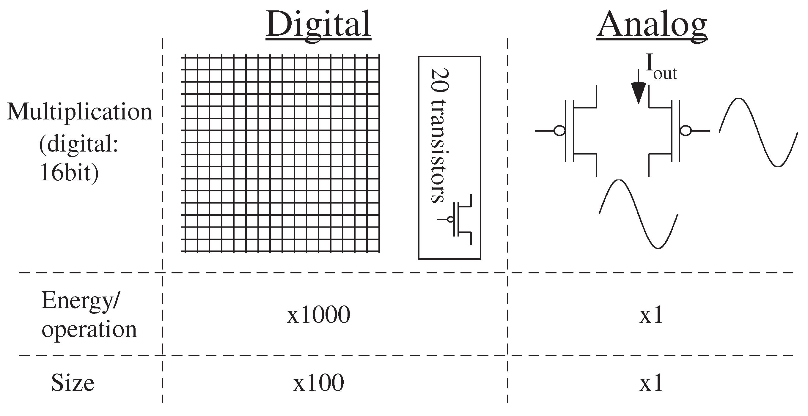
5. Analog Strength: Computational Effort (Energy) as a Metric for Digital and Analog Numerical Computation

The energetic resources required for either analog or digital need to serve as another metric for computation. This discussion interchanges energy and power consumption as required computation resources because embedded processing systems will continuously repeat the resulting operation at a required frequency. For digital systems, dynamic power is related to the required computation, and for analog systems, the computational power is related to the bias current programmed to its minimum functional level. Section 2 introduced the history of digital and analog computation, with an initial discussion of low-power computation (Section 2.2).
Figure 11 illustrates the energy and area (e.g., size/number of processors) comparison between digital and analog computation. This perspective started from Meads’s original work [11]. Roughly several thousand transistors are required for digital multiply (16 bit) (e.g., [78]) versus one to two transistors for an analog multiply, resulting in considerably lower capacitances to be charged and, therefore, lower required energy. Analog approaches are tuned through only a few FG devices per processing element. The transistor count also results in a 100× decrease in the required area. The small size of the processing elements enables many parallel structures, so one might get efficient processing by many slower computing units. Frequently, although not always, the analog devices are slightly larger to get better analog properties than minimum size digital devices.
Device to device mismatch limits the energy efficiency, as well as area efficiency and the performance of yield-constrained digital systems. The energy efficiency wall (introduced in Section 2) for digital computation [9], roughly around 10 MMAC(/s)/mW, is primarily constrained by device-to-device mismatch. Timing accuracy between digital logic gates is essential for reliable digital computation. Mismatch between MOSFETs causes considerable stress on any energy-efficient digital designer.
Figure 12a shows two identical inverters with V T 0 mismatch. Some recent efforts consider power supply ( V d d ) shifts for static operation considering V T 0 mismatch [79,80], but timing is rarely considered. FG tuned digital circuits, eliminating V T 0 mismatch (e.g., [81]), could be widespread, but to date, nothing beyond simple gates has been done other than the FG CLBs in the SoC FPAA structure.
Figure 12b shows the timing delays from a single inverter for a typical V T 0 mismatch (25.55 mV). The calculation modeled the two (saturated) nFET currents in Figure 12a, I 1 and I 2 , from the analytic EKV MOSFET model [82]:
I s = I t h l n 2 1 + e κ ( V d d V T 0 ) / 2 U T I 2 I 1 = e κ Δ V T 0 / U T   ( subthreshold ) .
where I t h is the current at threshold, κ is the gate voltage coupling into the MOSFET surface potential (assumed matched in this example) and U T is the thermal voltage. Subthreshold current biases would give the worst case mismatch (factor of two) in this example. Using classic transistor matching relations [83], with a transistor load capacitance ( C L o a d ), the energy and power (P) consumption are:
σ 2 1 W L ,   and   P C L o a d W L 1 σ 2 ,
showing that energy is directly related to transistor mismatch. The timing variance of a cascade of n inverters scales from its single inverter delay as n σ . The relationship would be similar for other logic gates. For a cascade of six inverters, operating at the threshold as in Figure 12b, the timing variance is nearly four-times the inverter delay, making a synchronous design nearly impossible to reliably complete timing.
Just decreasing transistor linewidth, without improving transistor mismatch results in no improvement in energy or power efficiency. For digital systems, this mismatch has not improved with transistor scaling since the 180-nm CMOS node [9]. Further, typical digital cells tend to keep the product of W and L relatively constant with scaling, getting better performance with decreasing L (increasing W / L ), but not improving the resulting energy efficiency. Although sub-threshold operation enables lower dynamic and static currents, without calibrating V T 0 mismatch, this region of operation likely results in worse overall performance. Further, digital systems utilizing large separate memory blocks further consume significant amount of power and energy, sometimes more than the computation being performed [43], making it difficult to notice that the energy required for computation may not have improved. Digital systems could use co-located computing and memory, although these techniques are rarely done in practice.
Lets consider a simple example comparing energy efficiency between digital and analog computation. We will assume digital computation for 32 bit (say single precision) arithmetic numbers close to the energy efficiency wall at four MMAC(/s)/mW. Consider the digital computation of a second order system,
τ 2 d 2 y d t 2 + τ Q d 2 y d t 2 + y = d x ( t ) d t
with acoustic input signals (<10-kHz frequency). To keep this problem manageable, assume moderate values of Q (0.5 to four) and τ = 1 ms. With samples every 50 μ s, three-digit (10 bit or 60 dB) output accuracy typically will require 20 Runga-Kutta 4 t h Order method (RK4) steps per iteration. The number of MAC operations per step will require roughly 10 MACs to evaluate an RK4 iteration, requiring four MMAC(/s), or 1 mW of power. The power required to supply the data for these computations is roughly two- to four-times larger than the computation itself. Measurements for analog computing systems of this computation result, for compiled systems, require less than 1 μ W of power for the same computation at the same output Signal-to-Noise Ratio (SNR) [1]. A digital filter approximation will require similar computation at the similar relative accuracy. The problem is a linear problem, minimizing the computational complexity; if a nonlinear ODE needs to be computed, any nonlinearities (e.g., sinh, tanh) will require significantly more MACs for the Taylor series approximations. The numerical noise for this calculation will eventually limit the numerical computation simulation time.

6. Simulation Tool Impact of Analog and Digital Numerics

Developing large-scale analog or digital computing systems, particularly energy-efficient computing systems, in a reasonable time frame requires some tools, as well as compilers. Digital tools, like MATLAB or compiled code libraries (e.g., Java), already abstract the numerical issues from the user, to the point engineers are unaware of the underlying numerics.
Some of the first analog/mixed-signal computing systems are emerging (e.g., [39]), including utilizing high-level graphical interfaces. Whether analog or digital computation, many aspects fit a similar framework in terms of component lists, net lists, compilation, place and route algorithms and the resulting targeting functions. While these aspects have room for improvement, their structure is similar between these two approaches.
The issue of simulation, using one system (digital) to emulate another system (physical) proves to be the largest computational challenge. Given that all synchronous digital computation can be related to a Turing machine, using a digital system to emulate another digital system seems reasonable, with the only issue a question of relative computational complexity between the real and emulation system. A digital system emulating an analog system requires digital simulation of at least ODEs, which we established is a challenging problem for digital systems. The potential higher computing level of analog systems (real values) compared with digital systems (countable values) further illustrates the numerical difficulty [13].
Issues with digital simulation of physical computing implies that the designer must resign themselves to simulating analog systems of moderate complexity, The functions modeling the circuits must have well-controlled derivatives and be analytic (continuous through all derivatives) to be well behaved for most numerical solutions. Physical computing systems tend to be advantageous for stiff numerical problems, and therefore, simulating these systems presents technical difficulties for numerical simulation. Noise modeling for analog computation is an essential aspect of system level simulation required for modeling measured responses. Analog system design tools already are starting to have this modeling [38]. This noise increases the derivatives of the function evaluation, further complicating the digital noise in the resulting system. Smaller digital simulations will enable initial performance right before actually compiling and computing using the physical medium, as well as helping to design/automate the resulting process providing the pathway to build higher level tools and metrics. Simulation of physical computing might require using other configurable physical computing systems [1,49].

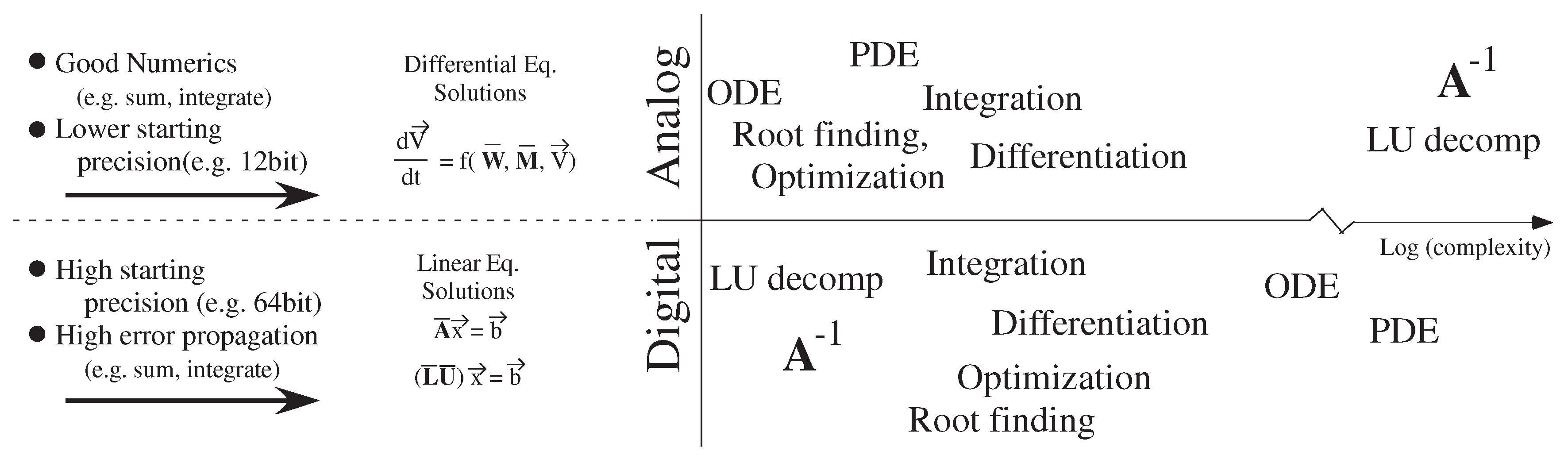
7. Comparing Analog and Digital Numerical Analysis Complexity

Figure 13 discusses the implication of the strengths and weaknesses of analog and digital computation. The different strengths in precision and numerics imply that digital systems lean towards algebraic matrix solutions and that analog systems lean towards ODE solutions. These results might translate to how one would plan a numerical analysis class. A traditional digital numerical analysis class would start from LU decomposition, moving to optimization and integration, and ending at ODE/PDE solutions.
Table 1 summarizes the properties of analog and digital computation systems. The algorithm tradeoff between analog and digital computation directly leads to the tradeoff between high-precision with poor numerics of digital computation verses the good numerics with lower precision of analog computation. Digital systems have relatively inexpensive high resolution (16, 32 or 64 bit), but with noisy numerics. Analog systems have higher cost for starting resolution (eight to 12 bits are typically reasonable), but with far less noisy numerical calculations. Because we are often dealing with embedded systems, energy/average power must be one metric (computation complexity at given resolution/power) for any consideration.
Digital computation focuses on problems with limited number of iterations that can embody high precision (e.g., 64-bit double precision), like LU decomposition (and matrix inversion). The LINPACK metric [64] makes complete sense to evaluate computing engines when the fundamental computing operations are LU decomposition. Classical digital numerical analysis courses begin with LU decomposition and move to significantly harder computations in optimization, ODE solutions and PDE solutions.
Analog computation solves difficult numerical applications that are tolerant of lower starting precision for computation, such as ODEs and PDEs. Simple operations like VMM are fairly similar in the tradeoffs between analog and digital approaches, particularly when using real-world sensor data starting off with lower precision (e.g., acoustic microphones at 60 dB, CMOS imaging at 50 to 60 dB, etc.). Many ODE and PDE systems have correlates in other physical systems found in nature that are the focus of high performance computing. The resulting time/area efficiencies for analog computation model a physical system by directly being the system to solve. This high-speed computation enables low-latency signal processing and control loops.
An analog numerical analysis class would start from ODE solutions, moving towards PDE, optimization and integration, and ending at algebraic matrix solutions. Ideal analog integration requires infinite gain, which is difficult to achieve due to the non-ideal effects of transistor current sources. Typically, good circuit techniques can minimize this low-frequency integration error. One would want to avoid analog LU decomposition where possible, while one wants to avoid solving a large number of ODEs and/or a couple of PDEs by digital methods. These two approaches show complimentary strengths and weaknesses, potentially opening opportunities when both systems are available.

8. Summary and Discussion

Analog design has come a long way from just saying lets do some magically inspired design with op-amps and a few resistors. Approaches towards analog programmability and configurability enable realistic conversations in this area. Digital computation relies on its strength in achieving relatively inexpensive high-precision, while analog computation relies on its strength in its well-behaved computational error propagation. Digital computation moves towards applications of (linear) algebraic solutions, while analog computation moves towards applications of ODE solutions. Table 2 summarizes these core frameworks and comparisons between analog and digital computation, as well as the open questions in these areas. The complimentary analog and digital computational techniques enable wider computational capabilities. This discussion is the first necessary step among many to follow towards a numerical physical-computing framework.
The analog numerical analysis is not contained by the range of applications for analog computation. The presence of analog numerical analysis theory is not advocating for a dogmatic view of only analog or digital computation. We need a framework for both approaches. The field of digital numerical analysis is looking at digital computation and how errors propagate for particular computations. It does not technically advocate for a particular computing system, but applicable where it is used. A large number of analog numerical analysis applications would be toward sensor processing and computation. The lower starting SNR (and effective bit size) of many sensors (eight to 12 bits) makes using analog computation highly advantageous.
The numerical analysis discussion asks what exactly made analog computing go from a dominant computing mechanism (1960s) to nearly irrelevant (1980s) twenty years later. The main reason was the lack of programmability. The ability to reuse the same digital system using abstracted frameworks (like Fortran) and the rapid growth of digital during the Moore’s law era enabled those who used the digital system to be different from those who designed the system. When one asks those who used analog computing in the 1960s, they are not surprised at the capabilities of analog devices, nor at the difficulties of memory or getting others to use their systems (e.g., moving cables). Additionally, they also agree that they had very little computational theory to utilize when building applications. Current analog computation’s ability to be reconfigured and programmed again changes these issues, potentially allowing for these analog computation techniques to be available in the engineer’s toolbox.
Mismatch of components was the second issue for analog computing, an issue solved by programmable analog concepts. Mismatch plagues any current analog approach that does not include reasonably fine-grained programming capability. Device mismatch shows in significant parameter errors, as well as is the main source of power supply fluctuations, temperature reference errors and linearity issues, resulting in effectively unmatched transistor devices relied upon for robust analog circuit design. Typically, eight-bit or more capability for adjusting component mismatch returns one sufficiently close to the typical textbook cases of matched transistor circuits. FG techniques directly adjust for the largest mismatch factor ( V T 0 ), and programmability directly improves offset, as well as power supply rejection and linearity errors (e.g., [84]). Previous studies (e.g., [68]) show that small mismatches between components typically have a small resulting system effect.
When programmability and elimination of mismatch are available capabilities, analog computing has manageable design constraints involving temperature effects, power supply variation, noise and linearity. The effects are typically of a similar size as, if not less than, noise constraints. For example, linearity effectively limits the maximum analog values, similar to digital limiting by register overflow; tradeoffs are made in analog or digital between computational noise and the resulting risk of overloading a particular value. Analog summation is not limited by linearity, but potentially computations preceding these computations and following after these computations. Using FG techniques, one can proportionally tradeoff linearity with energy consumed with no additional noise because of additional circuitry; therefore, one can use exactly the linearity needed for the problem and not spend any more energy than is necessary. With programmability, distortion is created by odd-symmetric nonlinearities. In the end, analog computation, with its lower starting resolution, but robust numerical capabilities, could find opportunities in many potential applications.

Acknowledgments

First, the author would like to thank my many students at Georgia Tech for numerous helpful conversations that helped this paper take shape. In particular, I appreciate the discussions with my recent students, Sahil Shah, Sihwan Kim and Aishwarya Natarajan, who have been involved in many of these discussions that formulated this paper. Second, I wish to thank Alan Feldstein, now Professor Emeritus, of Mathematics at Arizona State University, who taught me in many courses in numerical analysis and computer arithmetic. Without his inspirational teaching, I would never have had the appreciation for numerical analysis or computer arithmetic sufficient enough to embark in this effort.

Conflicts of Interest

The author declares no conflict of interest.

References

  1. George, S.; Kim, S.; Shah, S.; Hasler, J.; Collins, M.; Adil, F.; Wunderlich, R.; Nease, S.; Ramakrishnan, S. A Programmable and Configurable Mixed-Mode FPAA SoC. IEEE Trans. Very Large Scale Integr. Syst. 2016, 24, 2253–2261. [Google Scholar] [CrossRef]
  2. Wolf, W. Hardware-software co-design of embedded systems. Proc. IEEE 1994, 82, 967–989. [Google Scholar] [CrossRef]
  3. Jerraya, A.A.; Wolf, W. Hardware/Software Interface Codesign for Embedded Systems. IEEE Comput. 2005, 38, 63–69. [Google Scholar] [CrossRef]
  4. Teich, J. Hardware/Software Codesign: The Past, the Present, and Predicting the Future. Proc. IEEE 2012, 100, 1411–1430. [Google Scholar] [CrossRef]
  5. Sampson, A.; Bornholt, J.; Ceze, L. Hardware—Software Co-Design: Not Just a Cliché. In Advances in Programming Languages (SNAPL—15); Leibniz-Zentrum für Informatik: Wadern, Germany, 2015; pp. 262–273. [Google Scholar]
  6. Rossi, D.; Mucci, C.; Pizzotti, M.; Perugini, L.; Canegallo, R.; Guerrieri, R. Multicore Signal Processing Platform with Heterogeneous Configurable hardware accelerators. IEEE Trans. Very Large Scale Integr. Syst. 2014, 22, 1990–2003. [Google Scholar] [CrossRef]
  7. Zhao, Q.; Amagasaki, M.; Iida, M.; Kuga, M.; Sueyoshi, T. An Automatic FPGA Design and Implementation Framework. In Proceedings of the 23rd International Conference on Field Programmable Logic and Applications (FPL), Porto, Portugal, 2–4 September 2013; pp. 1–4. [Google Scholar]
  8. Weinhardt, M.; Krieger, A.; Kinder, T. A Framework for PC Applications with Portable and Scalable FPGA Accelerators. In Proceedings of the International Conference on Reconfigurable Computing and FPGAs (ReConFig), Cancun, Mexico, 9–11 December 2013; pp. 1–6. [Google Scholar]
  9. Marr, B.; Degnan, B.; Hasler, P.; Anderson, D. Scaling Energy Per Operation via an Asynchronous Pipeline. IEEE Trans. Very Large Scale Integr. Syst. 2013, 21, 147–151. [Google Scholar] [CrossRef]
  10. Degnan, B.; Marr, B.; Hasler, J. Assessing trends in performance per Watt for signal processing applications. IEEE Trans. Very Large Scale Integr. Syst. 2016, 24, 58–66. [Google Scholar] [CrossRef]
  11. Mead, C. Neuromorphic electronic systems. Proc. IEEE 1990, 78, 1629–1636. [Google Scholar] [CrossRef]
  12. Frantz, G.; Wiggins, R. Design case history: Speak and spell learns to talk. IEEE Spectr. 1982, 19, 45–49. [Google Scholar] [CrossRef]
  13. Hasler, J. Opportunities in Physical Computing driven by Analog Realization. In Proceedings of the IEEE International Conference on IEEE ICRC, San Deigo, CA, USA, 17–19 October 2016; pp. 1–8. [Google Scholar]
  14. Conte, S.D.; de Boor, C. Elementary Numerical Analysis: An Algorithmic Approach; McGraw Hill: New York, NY, USA, 1980. [Google Scholar]
  15. Butcher, J.C. Numerical Analysis of Ordinary Differential Equations: Runga Kutta and General Linear Methods; Wiley: Hoboken, NJ, USA, 1987. [Google Scholar]
  16. Mitchell, A.R.; Griffiths, D.F. The Finite Difference Method in Partial Differential Equations; Wiley: Hoboken, NJ, USA, 1980. [Google Scholar]
  17. Turing, R. On Computable Numbers. Proc. Lond. Math. Soc. 1937, 2, 230–265. [Google Scholar] [CrossRef]
  18. Mead, C.; Conway, L. VLSI Design; Addison Wesley: Boston, MA, USA, 1980. [Google Scholar]
  19. MacKay, D.M.; Fisher, M.E. Analogue Computing at Ultra-High Speed: An Experimental and Theoretical Study; John Wiley and Sons: New York, NY, USA, 1962. [Google Scholar]
  20. Karplus, W.J. Analog Simulation: Solution of Field Problems; McGraw Hill: New York, NY, USA, 1958. [Google Scholar]
  21. MacLennan, B.J. A Review of Analog Computing; Technical Report for University of Tennessee: Knoxville, TN, USA, 2007. [Google Scholar]
  22. Hopfield, J.J. Neural networks and physical systems with emergent collective computational abilities. Proc. Natl. Acad. Sci. USA 1982, 79, 2554–2558. [Google Scholar] [CrossRef] [PubMed]
  23. Hopfield, J.J. Neurons with graded responses have collective computational properties like those of two-state neurons. Proc. Natl. Acad. Sci. USA 1984, 81, 3088–3092. [Google Scholar] [CrossRef] [PubMed]
  24. Mead, C. Analog VLSI and Neural Systems; Addison Wesley: Boston, MA, USA, 1989. [Google Scholar]
  25. Hasler, P.; Diorio, C.; Minch, B.A.; Mead, C.A. Single transistor learning synapses. In Advances in Neural Information Processing Systems 7; Tesauro, G., Touretzky, D.S., Todd, K.L., Eds.; MIT Press: Cambridge, MA, USA, 1994; pp. 817–824. [Google Scholar]
  26. Kim, S.; Hasler, J.; George, S. Integrated Floating-Gate Programming Environment for System-Level ICs. IEEE Trans. Very Large Scale Integr. Syst. 2016, 24, 2244–2252. [Google Scholar] [CrossRef]
  27. Srinivasan, V.; Serrano, G.J.; Gray, J.; Hasler, P. A precision CMOS amplifier using floating-gate transistors for offset cancellation. IEEE J. Solid-State Circuits 2007, 42, 280–291. [Google Scholar] [CrossRef]
  28. Srinivasan, V.; Serrano, G.; Twigg, C.M.; Hasler, P. A floating-gate- based programmable CMOS reference. IEEE Trans. Circuits Syst. I Regul. Pap. 2008, 55, 3448–3456. [Google Scholar] [CrossRef]
  29. Hasler, P. Continuous-time feedback in floating-gate MOS circuits. IEEE Trans. Circuits Syst. Analog Digit. Signal Process. 2001, 48, 56–64. [Google Scholar] [CrossRef]
  30. Hasler, P.; Minch, B.; Diorio, C. An autozeroing floating-gate amplifier. IEEE Trans. Circuits Syst. Analog Digit. Signal Process. 2001, 48, 74–82. [Google Scholar] [CrossRef]
  31. Brink, S.; Hasler, J.; Wunderlich, R. Adaptive floating-gate circuit enabled large-scale FPAA. IEEE Trans. Very Large Scale Integr. Syst. 2014, 22, 2307–2315. [Google Scholar] [CrossRef]
  32. Laiho, M.; Hasler, J.; Zhou, J.; Du, C.; Lu, W.; Lehtonen, E.; Poikonen, J. FPAA/memristor hybrid computing infrastructure. IEEE Trans. Circuits Syst. I Regul. Pap. 2015, 62, 906–915. [Google Scholar] [CrossRef]
  33. Hasler, J.; Shah, S. Reconfigurable Analog PDE Computation for Baseband and RF Computation. In Proceedings of the GOMAC, Reno, NV, USA, 20–23 March 2017. [Google Scholar]
  34. Ozalevli, E.; Huang, W.; Hasler, P.E.; Anderson, D.V. A reconfigurable mixed-signal VLSI implementation of distributed arithmetic used for finite impulse response filtering. IEEE Trans. Circuits Syst. I Regul. Pap. 2008, 55, 510–521. [Google Scholar] [CrossRef]
  35. Gregorian, R.; Temes, G.C. Analog MOS Integrated Circuits for Signal Processing; Wiley: Hoboken, NJ, USA, 1983. [Google Scholar]
  36. Ramakrishnan, S.; Wunderlich, R.; Hasler, J.; George, S. Neuron array with plastic synapses and programmable dendrites. IEEE Trans. Biomed. Circuits Syst. 2013, 7, 631–642. [Google Scholar] [CrossRef] [PubMed]
  37. Wunderlich, R.; Adil, F.; Hasler, P. Floating gate-based field programmable mixed-signal array. IEEE Trans. Very Large Scale Integr. Syst. 2013, 21, 1496–1505. [Google Scholar] [CrossRef]
  38. Schlottmann, C.; Hasler, J. High-level modeling of analog computational elements for signal processing applications. IEEE Trans. Very Large Scale Integr. Syst. 2014, 22, 1945–1953. [Google Scholar] [CrossRef]
  39. Collins, M.; Hasler, J.; George, S. An Open-Source Toolset Enabling Analog–Digital Software Codesign. J. Low Power Electron. Appl. 2016, 6, 3. [Google Scholar] [CrossRef]
  40. Hasler, J.; Kim, S.; Shah, S.; Adil, F.; Collins, M.; Koziol, S.; Nease, S. Transforming Mixed-Signal Circuits Class through SoC FPAA IC, PCB, and Toolset. In Proceedings of the IEEE European Workshop on Microelectronics Education, Southampton, UK, 11–13 May 2016. [Google Scholar]
  41. Hasler, J.; Kim, S.; Adil, F. Scaling Floating-Gate Devices predicting behavior for Programmable and Configurable Circuits and Systems. J. Low Power Electron. Appl. 2016, 6, 13. [Google Scholar] [CrossRef]
  42. Hasler, J.; Shah, S. Learning for VMM + WTA Embedded Classifiers; GOMAC: Orlando, FL, USA, March 2016. [Google Scholar]
  43. Hasler, J.; Marr, H.B. Finding a roadmap to achieve large neuromorphic hardware systems. Front. Neurosci. 2013, 7. [Google Scholar] [CrossRef] [PubMed]
  44. Hall, T.; Twigg, C.; Gray, J.; Hasler, P.; Anderson, D. Large-scale Field-Programmable Analog Arrays for analog signal processing. IEEE Trans. Circuits Syst. 2005, 52, 2298–2307. [Google Scholar] [CrossRef]
  45. Peng, S.Y.; Gurun, G.; Twigg, C.M.; Qureshi, M.S.; Basu, A.; Brink, S.; Hasler, P.E.; Degertekin, F.L. A large-scale Reconfigurable Smart Sensory Chip. In Proceedings of the IEEE International Symposium on Circuits and Systems, Taipei, Taiwan, 24–27 May 2009; pp. 2145–2148. [Google Scholar]
  46. Twigg, C.M.; Gray, J.D.; Hasler, P. Programmable floating gate FPAA switches are not dead weight. In Proceedings of the IEEE International Symposium on Circuits and Systems, New Orleans, LA, USA, 27–30 May 2007; pp. 169–172. [Google Scholar]
  47. Schlottmann, C.; Hasler, P. A highly dense, low power, programmable analog vector-matrix multiplier: The FPAA implementation. IEEE J. Emerg. Sel. Top. Circuits Syst. 2011, 1, 403–411. [Google Scholar] [CrossRef]
  48. Rumberg, B.; Graham, D.W. Reconfiguration Costs in Analog Sensor Interfaces for Wireless Sensing Applications. In Proceedings of the International Midwest Symposium on Circuits and Systems (MWSCAS), Columbus, OH, USA, 4–7 August 2013; pp. 321–324. [Google Scholar]
  49. Guo, N.; Huang, Y.; Mai, T.; Patil, S.; Cao, C.; Seok, M.; Sethumadhavan, S.; Tsividis, Y. Energy-efficient hybrid analog/digital approximate computation in continuous time. IEEE J. Solid-State Circuits 2016, 51, 1514–1524. [Google Scholar] [CrossRef]
  50. Shyu, J.B.; Temes, G.C.; Krummenacher, F. Random error effects in matched MOS capacitors and current sources. IEEE J. Solid-State Circuits 1984, 19, 948–956. [Google Scholar] [CrossRef]
  51. Lyon, R.F.; Mead, C. An analog electronic cochlea. IEEE Trans. Acoust. Speech Signal Process. 1988, 36, 1119–1134. [Google Scholar] [CrossRef]
  52. Watts, L.; Kerns, D.A.; Lyon, R.F.; Mead, C.A. Improved implementation of the silicon cochlea. IEEE J. Solid-State Circuits 1992, 27, 692–700. [Google Scholar] [CrossRef]
  53. Van Schaik, A.; Fragniere, E.; Vittoz, E.A. Improved silicon cochlea using compatible lateral bipolar transistors. In Neural Information Processing Systems; Touretzky, D.S., Hasselmo, M.E., Eds.; MIT Press: Cambridge, MA, USA, 1996; pp. 671–677. [Google Scholar]
  54. Hosticka, B.J. Performance comparison of analog and digital circuits. Proc. IEEE 1985, 73, 25–29. [Google Scholar] [CrossRef]
  55. Vittoz, E.A. Future of analog in the VLSI environment. In Proceedings of the International Symposium on Circuits and Systems, New Orleans, LA, USA, 1–3 May 1990; Volume 2, pp. 1347–1350. [Google Scholar]
  56. Sarpeshkar, R. Analog Versus Digital: Extrapolating from Electronics to Neurobiology. Neural Comput. 1998, 10, 1601–1638. [Google Scholar] [CrossRef] [PubMed]
  57. Abshire, P.A. Sensory Information Processing under Physical Constraints. Ph.D. Thesis, Johns Hopkins University, Baltimore, MD, USA, 2001. [Google Scholar]
  58. Hasler, P.; Smith, P.; Graham, D.; Ellis, R.; Anderson, D. Analog floating-gate, on-chip auditory sensing system interfaces. IEEE Sens. J. 2005, 5, 1027–1034. [Google Scholar] [CrossRef]
  59. Vittoz, E.A. Low-power design: Ways to approach the limits. In Proceedings of the IEEE International Solid-State Circuits Conference, San Francisco, CA, USA, 6–18 February 1994; pp. 14–18. [Google Scholar]
  60. Sarpeshkar, R.; Delbruck, T.; Mead, C. White noise in MOS transistors and resistors. IEEE Circuits Devices Mag. 1993, 9, 23–29. [Google Scholar] [CrossRef]
  61. Kim, S.; Shah, S.; Hasler, J. Calibration of Floating-Gate SoC FPAA System. IEEE Trans. Very Large Scale Integr. Syst. 2017. in Press. [Google Scholar]
  62. Shapero, S.; Hasler, P. Mismatch characterization and calibration for accurate and automated analog design. IEEE Trans. Circuits Syst. I Regul. Pap. 2013, 60, 548–556. [Google Scholar] [CrossRef]
  63. Vittoz, E.A. Analog VLSI Signal Processing: Why, Where and How? J. VLSI Signal Process. 1994, 8, 27–44. [Google Scholar] [CrossRef]
  64. Dongarra, J.J.; Luszczek, P.; Petitet, A. The LINPACK Benchmark: Past, present and future. Concurr. Comput. Pract. Exp. 2003, 15, 803–820. [Google Scholar] [CrossRef]
  65. Widrow, B. Adaptive Filters I: Fundamentals; Technical Report No. 6764-6; Stanford University: Stanford, CA, USA, 1966. [Google Scholar]
  66. Widrow, B.; Lehr, M.A. 30 Years of Adaptive Neural Networks: Perceptrons, Madaline, and Backpropagation. Proc. IEEE 1990, 78, 1415–1442. [Google Scholar] [CrossRef]
  67. Schneider, C.; Card, H. CMOS implementation of analog hebbian synaptic learning circuits. In Proceedings of the IEEE IJCNN-91-Seattle International Joint Conference on Neural Networks, Seattle, WA, USA, 8–12 July 1991; pp. 437–442. [Google Scholar]
  68. Hasler, P.; Akers, L. Circuit implementation of trainable neural networks employing both supervised and unsupervised techniques. In Proceedings of the IEEE International Joint Conference on Neural Networks, San Diego, CA, USA, 10–13 May 1992; pp. 1565–1568. [Google Scholar]
  69. Hasler, P.; Dugger, J. An analog floating-gate node for supervised learning. IEEE Trans. Circuits Syst. I Regul. Pap. 2005, 52, 834–845. [Google Scholar] [CrossRef]
  70. Ramakrishnan, S.; Hasler, J. Vector-Matrix Multiply and WTA as an Analog Classifier. IEEE Trans. Very Large Scale Integr. Syst. 2014, 22, 353–361. [Google Scholar] [CrossRef]
  71. Morton, K.W.; Mayers, D.F. Numerical Solution of Partial Differential Equations; Cambridge University Press: Cambridge, UK, 2005. [Google Scholar]
  72. George, S.; Hasler, J.; Koziol, S.; Nease, S.; Ramakrishnan, S. Low power dendritic computation for wordspotting. J. Low Power Electron. Appl. 2013, 3, 73–98. [Google Scholar] [CrossRef]
  73. Koziol, S.; Brink, S.; Hasler, J. A neuromorphic approach to path planning using a reconfigurable neuron array IC. IEEE Trans. Very Large Scale Integr. Syst. 2014, 22, 2724–2737. [Google Scholar] [CrossRef]
  74. Koziol, S.; Wunderlich, R.; Hasler, J.; Stilman, M. Single-Objective Path Planning for Autonomous Robots Using Reconfigurable Analog VLSI. IEEE Trans. Syst. Man Cybern. Syst. 2017, 47, 1301–1314. [Google Scholar] [CrossRef]
  75. Nease, S.; George, S.; Hasler, P.; Koziol, S.; Brink, S. Modeling and implementation of voltage-mode CMOS dendrites on a reconfigurable analog platform. IEEE Trans. Biomed. Circuits Syst. 2012, 6, 76–84. [Google Scholar] [CrossRef] [PubMed]
  76. Whitham, G.B. Linear and Nonlinear Waves; Wiley: Hoboken, NJ, USA, 1973. [Google Scholar]
  77. Kevorkian, J.; Cole, J.D. Perturbation Methods in Applied Mathematics; Springer: New York, NJ, USA, 1981. [Google Scholar]
  78. Asadi, P.; Navi, K. A New Low Power 32 × 32-bit Multiplier. World Appl. Sci. J. 2007, 2, 341–347. [Google Scholar]
  79. Fuketa, H.; Iida, S.; Yasufuku, T.; Takamiya, M.; Nomura, M.; Shinohara, H.; Sakurai, T. A Closed-form Expression for Estimating Minimum Operating Voltage (VDDmin) of CMOS Logic Gates. In Proceedings of the Design Automation Conference, San Diego, CA, USA, 5–10 June 2011; pp. 984–989. [Google Scholar]
  80. Fuketa, H.; Yasufuku, T.; Iida, S.; Takamiya, M.; Nomura, M.; Shinohara, H.; Sakurai, T. Device-Circuit Interactions in Extremely Low Voltage CMOS Designs. In Proceedings of the 2011 IEEE International Electron Devices Meeting (IEDM), Washington, DC, USA, 5–7 December 2011; pp. 559–562. [Google Scholar]
  81. Degnan, B.P.; Wunderlich, R.B.; Hasler, P. Programmable floating-gate techniques for CMOS inverters. In Proceedings of the IEEE International Symposium on Circuits and Systems, Kobe, Japan, 23–26 May 2005; pp. 2441–2444. [Google Scholar]
  82. Enz, C.C.; Krummenacher, F.; Vittoz, E.A. An analytical MOS transistor model valid in all regions of operation and dedicated to low-voltage and low-current applications. Analog Integr. Circuits Signal Process. 1995, 8, 83–114. [Google Scholar] [CrossRef]
  83. Pelgrom, M.J.M.; Duinmaijer, A.C.J.; Welbers, A.P.G. Matching Properties of MOS Transistors. IEEE J. Solid State Circuits 1989, 24, 1433–1440. [Google Scholar] [CrossRef]
  84. Adil, F.; Serrano, G.; Hasler, P. Offset removal using floating-gate circuits for mixed-signal systems. In Proceedings of the Southwest Symposium on Mixed-Signal Design, Las Vegas, NV, USA, 23–25 February 2003; pp. 190–195. [Google Scholar]
Figure 1. When starting from potential programmable and configurable analog and digital computational capabilities, an engineer must discern the right capabilities for particular parts of her/his application. Analog numerical analysis complimenting digital numerical analysis provides the framework to optimize application opportunities.
Jlpea 07 00017 g001
Figure 2. Digital and analog computation approaches based on their fundamental framework (or lack of it). Digital computation builds from the framework of Turing machines, setting up the capability of computer architectures, computer algorithms and resulting numerical analysis. This framework becomes the basis for our day to day digital computing, such as laptop computing. Analog computation is perceived to have little computational modeling, as well as architectures and algorithms. The resulting analog computing designs, where built, seem more like bottom-up artwork rather than top-down digital computing design.
Jlpea 07 00017 g002
Figure 3. SoC large-scale Field Programmable Analog Array (FPAA) device and comparison of power-efficient computational techniques in MAC (/s)/W, including digital, analog Signal Processing (SP) techniques, and the potential for neuromorphic physical algorithms. There have been amazing improvements of three orders of magnitude in digital technology from speak-and-spell devices [12] to current day smart phones. The analog SP approaches have the promise of similar advancements by three orders of magnitude, as they become a stable capability. Biological neurons show a potential of five more orders of magnitude of improvement, opening further opportunity for efficient computational devices.
Jlpea 07 00017 g003
Figure 4. A typical measurement setup for SoC FPAA devices. The interface is a USB port to communicate with and power the resulting board. Additional resources (like a Digilent function generator + scope) can be easily used for further characterization.
Jlpea 07 00017 g004
Figure 5. Classical plot of the impact of resolution (single component SNR) versus its resulting analog (polynomial) or digital (logarithmic) cost. The equivalent bits of resolution are log 2 (SNR). SNR is defined at the ratio of the largest signal, limited by hard limits or linearity, to the smallest signal, limited by noise. Mismatch is recognized as a fundamental limitation for analog circuit precision (crossover between five and eight bits). Using programmable Floating-Gate (FG) techniques enable crossover points past classical levels to typical ranges between 10and 14 bits of SNR.
Jlpea 07 00017 g005
Figure 6. FG parameters result in significantly higher parameter density (100× or larger). We compare between FG parameters and the next closest solution, having an n-bit DAC at every device. Optimistically, a DAC grows by a factor of two for an increase of one bit. At eight-bit DAC precision, 100 FG parameters is smaller than 1 DAC for 350-nm CMOS. We assume an increase for a DAC of 2× for one bit. Typically, the cost will increase at a higher level. Handling mismatch is a key risk for any analog (as well as digital) system; only programmability makes analog computation practical in a system (including high precision ADCs).
Jlpea 07 00017 g006
Figure 7. Illustration of basic computing operations, summation and integration, between analog and digital approaches. Analog approaches tend to be nearly ideal in these situations, where digital approaches accumulate significant noise and headroom errors in these processes. Analog approaches need to be aware how these operations interface with the rest of the computation circuitry.
Jlpea 07 00017 g007
Figure 8. Classical picture for numerical integration (second order) or ODE solution as a function of step size. Initially, error decreases as step size decreases due to the resulting order of the algorithm. As one continues to decrease the step size, accumulated errors due to numerical noise become noticeable and eventually become the dominant source of error.
Jlpea 07 00017 g008
Figure 9. Required numerical requirements for digital and analog adaptive filter computations. Adaptive filters are two-timescale operations, with a fast timescale for signal computation (20 Hz to 20 kHz for speech computation) and a slow timescale for adaptation (<1 Hz for speech), with separation between the two timescales.
Jlpea 07 00017 g009
Figure 10. Example of analog computing. (a) Implementation of a one-dimensional ladder filter for computing inductor (L) and capacitor (C) lines. These components can be implemented in CABs or as part of routing. (b) Measured data for a sine-wave input (5 kHz) to a 10-tap ladder filter implemented on the SoC FPAA (350 nm IC).
Jlpea 07 00017 g010
Figure 11. Physical argument of analog versus digital computational efficiency, originating with Mead’s original work [11]. A 16-bit digital and 12-bit analog multiplication + addition have similar accuracy after a small length VMM operation. A digital multiplication requires roughly 5000 or more transistors and greater than 1000 capacitors to charge per multiplication (e.g., [78]). Because analog devices tend to be slightly larger than digital devices to get more ideal characteristics, the area improvements are typically factors of 100. The two approaches use similar power supplies, where the analog is enabled by programmable analog approaches.
Jlpea 07 00017 g011
Figure 12. Effect of mismatch for digital circuits; mismatch limits the performance of yield-constrained digital circuits. (a) Two identically-drawn CMOS inverters, transitioning between a one ( V d d ) and a zero (GND) that differ by V T 0 mismatch between the devices. The nFET devices act mostly like current sources to decrease the voltage; the capacitive loads are matched. The measurement would have two different fall times due to the mismatch, although the designer was hoping for identical responses. (b) Calculated inverter timing mismatch as a function of bias current. Given that two nFETs are required for this comparison, mismatch in V T 0 of 25.55 mV is routine for small devices even for 350-nm CMOS processes.
Jlpea 07 00017 g012
Figure 13. Analog computation utilizes strong numerics to empower its lower starting precision; digital computation utilizes high starting precision to empower its higher (relative) numerical noise. Fundamental operation for digital systems are solutions of linear equations, where the fundamental operations for analog systems are solutions of differential equations. The resulting complexity for digital and analog approaches takes complimentary paths.
Jlpea 07 00017 g013
Table 1. Summary of digital and analog computational approaches. VMM, Vector-Matrix Multiplication.
DigitalAnalog
PrecisionHigh starting precision, low cost adding morelower starting precision (e.g., 10, 12, 14 bit)
Summation NoiseHigh numerical noise accumulation (summation)ideal summation
Latencycomputational latency (need for pipelining)minimal latency
Computational Efficiency (VMM)10 MMAC (/s)/mW (32 bit)10 MMAC (/s)/ μ W (×1000, 12 bit)
Intellectual TraditionLong numerical traditiona few artistic experts, sometimes agree
Table 2. Summary of Framework and comparisons between analog and digital computation.
Digital StrengthAnalog Strength
Lower Cost Numerical PrecisionXFG helps
Low Error Numerical Operations X
Core Numerical AlgorithmLU decompositionODE solutions
Computational Energy Required X
Designer Knowledge, Number Tools now
of Designers, CAD toolsXbeing developed

