Article

Stochastic-Based Spin-Programmable Gate Array with Emerging MTJ Device Technology

1
Computer Engineering Program, California State University, Fullerton, CA 92831, USA
2
Department of Electrical and Computer Engineering, University of Central Florida, Orlando, FL 32817, USA
*
Author to whom correspondence should be addressed.
J. Low Power Electron. Appl. 2016, 6(3), 15; https://doi.org/10.3390/jlpea6030015
Submission received: 17 May 2016 / Revised: 28 July 2016 / Accepted: 29 July 2016 / Published: 12 August 2016
(This article belongs to the Special Issue Recent Advances in Emerging Low Power Circuits and Systems)

Abstract

:
This paper describes the stochastic-based Spin-Programmable Gate Array (SPGA), an innovative architecture attempting to exploit the stochastic switching behavior newly found in emerging spintronic devices for reconfigurable computing. While many recently studies have investigated using Spin Transfer Torque Memory (STTM) devices to replace configuration memory in field programmable gate arrays (FPGAs), our study, for the first time, attempts to use the quantum-induced stochastic property exhibited by spintronic devices directly for reconfiguration and logic computation. Specifically, the SPGA was designed from scratch for high performance, routability, and ease-of-use. It supports variable-granularity multiple-input-multiple-output (MIMO) logic blocks and variable-length bypassing interconnects with a symmetrical structure. Due to its unconventional architectural features, the SPGA requires several major modifications to be made in the standard VPR placement/routing CAD flow, which include a new technology mapping algorithm based on computing (k, l)-cut, a new placement algorithm, and a modified delay-based routing procedure.Previous studies have shown that, simply replacing reconfiguration memory bits with spintronic devices, the conventional 2D island-style FPGA architecture can achieve approximately 5 times area savings, 2 times speedup and 1.6 times power savings. Our mixed-mode simulation results have shown that, with FPGA architecture innovations, on average, a SPGA can further achieve more than 10 times improvement in logic density, about 5 times improvement in average net delay, and about 5 times improvement in the critical-path delay for the largest 12 MCNC benchmark circuits over an island-style baseline FPGA with spintronic configuration bits.

Graphical Abstract

1. Introduction

Emerging spintronic devices, such as spin-valves and domain-wall magnets (DWM), have rekindled significant research interests in novel circuit and architecture design methodologies [1,2]. Sharply deviating from CMOS device technology, spintronic devices use spin transfer torque, instead of charge, as the medium of information processing, therefore offering not only ultra-low critical current (e.g., ≤100 μ A at 65 nm), simple switching scheme, and ultra-fast-speed, but also many fascinating probabilistic-related physical properties [3,4,5,6]. In particular, as shown in Figure 1a, Magnetic Tunnel Junctions (MTJ), the cornerstone of spintronic devices, can be densely embedded into CMOS logic circuits and fabricated with extremely small footprint on top of the metal layers and occupy almost “zero” chip area. Therefore, a hybrid MTJ-CMOS chip is considered by many as a potentially powerful solution that brings non volatility, instant on/off, and low standby power to today’s integrated circuit technology.
Recently, in the arena of FPGA research, studies on exploiting Spin Transfer Torque Magnetisation (STTM) switching devices have surged. For example, newly emerging memristor devices have been investigated to replace SRAM as the storage of elements in CMOS-based FPGA [8]. More recently, the nano crossbar architecture has been touted [9,10,11]. as an even more superior alternative to the conventional non-volatile phase-change memory due to its high density and lower power consumption [12,13]. Another conceptually appealing approach to directly applying MTJ-CMOS devices is to stack the programming overhead of an FPGA on top of the logic blocks and interconnect layers that would be implemented in a state-of-the-art CMOS technology. This approach resembles the monolithically stacked 3D-FPGA architecture, as depicted in Figure 1b, which achieves significant performance benefits [7,14]. Besides the obvious benefit of higher logic density, vertical stacking with a hybrid MTJ-CMOS device can potentially reduce interconnect length, hence reducing signal path delay and power consumption and offers a possible route to closing the performance gap between FPGAs and cell-based ASICs. However, the vast majority of these studies have focused on using spintronic devices as storage elements and configuration memory bits, therefore achieving low power dissipation and high speed without making significant changes to the conventional FPGA architecture and circuit design.
In this study, we attempt to directly use the inherent quantum-induced stochastic property of spintronic devices, not merely as memory storage, but for logic computation. Together with other researchers [15,16], we strongly believe that, without more innovations in FPGA architecture, the advance in device technology alone can not fully shrink the significant performance gap between FPGA and ASIC devices. The major motivation behind our study is to solve the following two well-known FPGA architecture design challenges, which can not simply be tackled by replacing conventional SRAM-based memory bits in a modern FPGA chip with the emerging spintronic devices, such as MTJs (Magnetic Tunnel Junction).
The first major challenge in FPGA architecture design is to determine the granularity of logic blocks in an FPGA. All prominent FPGAs [17,18,19,20] today have fixed and uniform logic granularity for each logic block. From the architecture point of view, coarse-grain blocks have much less stress on the placement and routing but often result in long internal logic delays and under-utilization for designs in small size, whereas fine-grain logic blocks can achieve shorter internal delay but often requires excessive amount of routing resource in order to successfully route a circuit. From the application point of view, data-path functions, in particular arithmetic functions, often operate on coarser arguments than control-path logic and are usually realized by fine-grain logic elements, while the implementation of control-path logic mostly benefits from coarser granularity. A rather interesting question is whether the logic blocks in an FPGA should be heterogeneous or homogeneous in size.
The second challenge is to determine the optimal segmentation of routing interconnects. In conventional routing architecture, each routing channel consists of a group of interconnects with variable lengths. For example, Virtex II [18] has 16 Single, 40 Double, 120 HEX, and 24 long interconnects in each routing channel. In general, short segments are advantageous to routability but bad for delay and power performance, while long interconnects achieve better delay performance but may result higher power consumptions. For a given set of benchmark circuits, what is exactly the optimal segmentation for a particular routing architecture remains an open question.
We propose the stochastic-based Spin-programmable Gate Array (SPGA) architecture to meet the above design challenges. Our objective is to develop an architecture that maximizes the application spectrum for both data-path and control-path applications without compromising performance and area efficiency, while fully exploiting the performance benefits entailed by the emerging MTJ devices, especially its inherent quantum-induced stochastic switching. The central idea of SPGA is to design and implement stochastic-based programmable logic blocks (SLB) in order to replace the traditional lookup-based (LUT) logic blocks. In addition, both the granularity and the input-output numbers of the new logic blocks can be dynamically configurable on a per-mapping basis at configuration time. More specifically, our major contributions include:
  • We invented a new curve-based method to reinterpret and redefine Boolean logic functions, therefore can efficiently implement multiple-input-multiple-output logic block without noticeable hardware usage overheads. This technique compounds the overall performance benefits resulting from the MTJ devices.
  • Taylor expansion, although mathematically elegant and powerful, has never been considered in hardware-assisted functional evaluation due to its excessive hardware cost. Our stochastic-based approach natively exploits the inherent Gaussian-like stochastic switching behavior of the emerging spintronic devices, therefore bypassing the excessive hardware overhead of Boolean-based methodology.
  • Due to the SPGA’s unconventional architectural features, we have made several modifications to the existing academic-grade software flow of logic synthesis, technology mapping, placement, and routing. In particular, given the freedom of configuring the output number of SLBs, we developed a variant of the conventional technology mapping algorithm based on computing (k, l)-feasible cuts.
The rest of our paper is organized as follows. In Section 2, we briefly overview the overall architecture of the Spin-Programmable Gate Array (SPGA). We then illustrate in Section 3 how a stochastic-based logic block (SLB) can be constructed with MTJ devices. In particular, We review the newly discovered stochastic switching behavior of Magnetic Tunneling Junctions (MTJ) and discuss the circuit design of a typical SLB. In Section 5, we detail each necessary module for logic synthesis, placement, and routing of SPGA. The performance comparison results of three performance metrics (hardware usage, delay, and energy consumption) between the SPGA architecture and three other island-style baseline FPGAs in Section 6. The error analysis are performed in Section 7. Finally, in Section 8, we summarize our findings and comment on several open research problems related to the SPGA architecture.

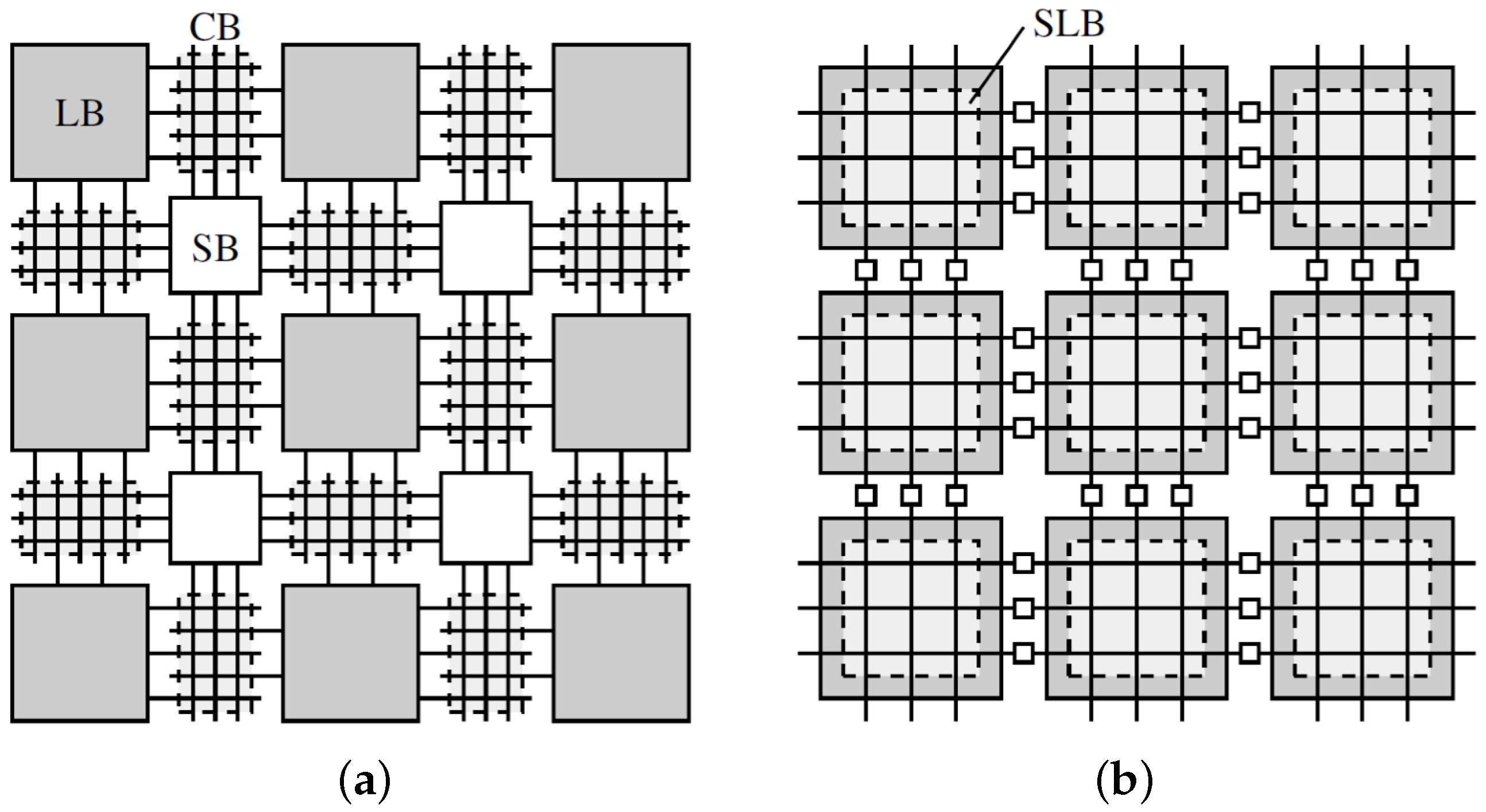
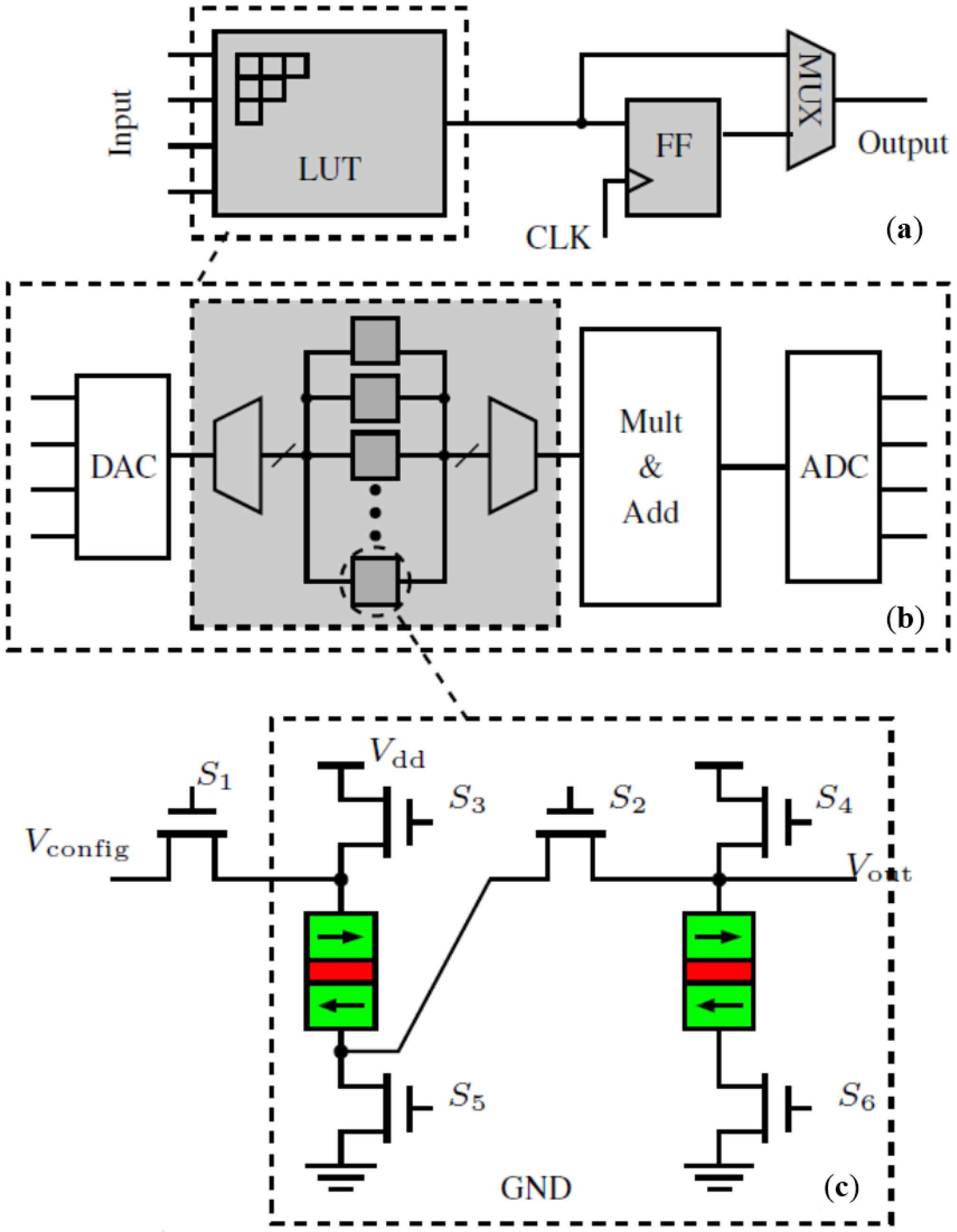
2. Architecture Overview

To a large extent, the architecture of SPGA resembles that of the conventional well-structured island style FPGA as shown in Figure 2a, in which an array of logic blocks (called Configurable Logic Block, CLB, or Logic Array Block, LAB, depending on vendor) are surrounded by pre-fabricated programmable routing channels and I/O pads. However, the SPGA architecture depicted in Figure 2b differs from the existing norm in at least two aspects. First, in the traditional CMOS-based FPGA technology, all configurable bits are implemented with memory devices such as 6-T SRAM. In the SPGA, we do not use binary bits to “define” our target logic function. Instead, we use the spin-based magnetization to configure the logic blocks. Second, the functionality of the memory-based LUT hinges on the concept of K-map and is based on the Boolean algebra. In a sharp contrast, the stochastic-based LUT uses a new curve-based method to reinterpret and redefine Boolean logic functions, therefore can efficiently implement a logic block with a configurable number of logic inputs and outputs without negatively causing excessive hardware overheads. Finally, given the 3D “nature” of the MTJ-CMOS hybrid device technology, we can redesign the interconnect architecture of the SPGA. Specifically, the LB inputs and outputs connect first to local segments. These segments can then be programmable connected to segments in neighboring routing blocks and/or to interconnect segments in a routing channels via programmable buffers and muxes with buffered outputs. The interconnect segments can be directly connected to form longer segments using programmable buffers without going through routing blocks (we shall refer to such interconnects as bypass interconnects).

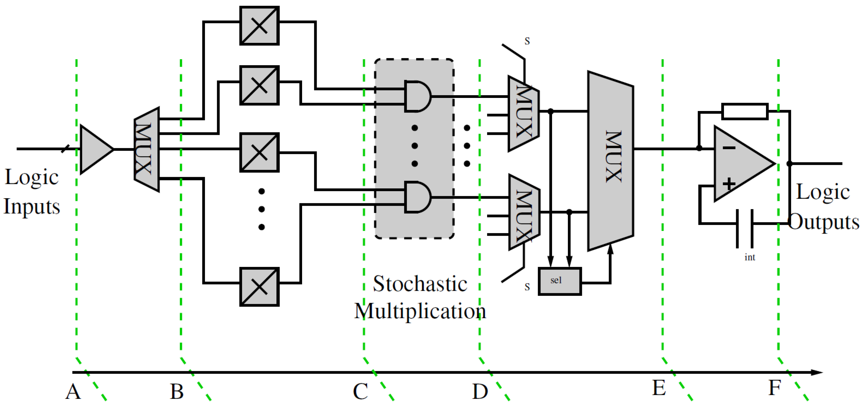
3. Stochastic-Based Logic Block (SLB)

One of the most important foundations in modern FPGA technology is the concept of Lookup-Table (LUT), which acts as a hardware implementation of K-map that directly performs reconfigurable logic functions. In Subsection 3.1, we present a new perspective to reinterpreting the K-Map in an algebraic way based on encoded logic inputs and outputs. Furthermore, we propose to use the well-known Taylor expansion to implement this new function evaluation method with hardware. However, with CMOS device technology, our new replacement to SRAM-based LUT may be too expensive in hardware usage. therefore, in Subsection 3.2, we introduce the newly-established stochastic switching behavior in MTJ devices and demonstrate how to build a reconfigurable random sample generator efficiently with them. Finally in Subsection 3.3, we we show how to take advantage of the stochastic switching behavior of emerging spintronic devices to natively perform curve fitting with ultra-low energy consumption, thus fulfilling logic functions. We present the complete circuit of our stochastic-based logic block (SLB) and validate its correct operation with mixed-mode circuit simulations.

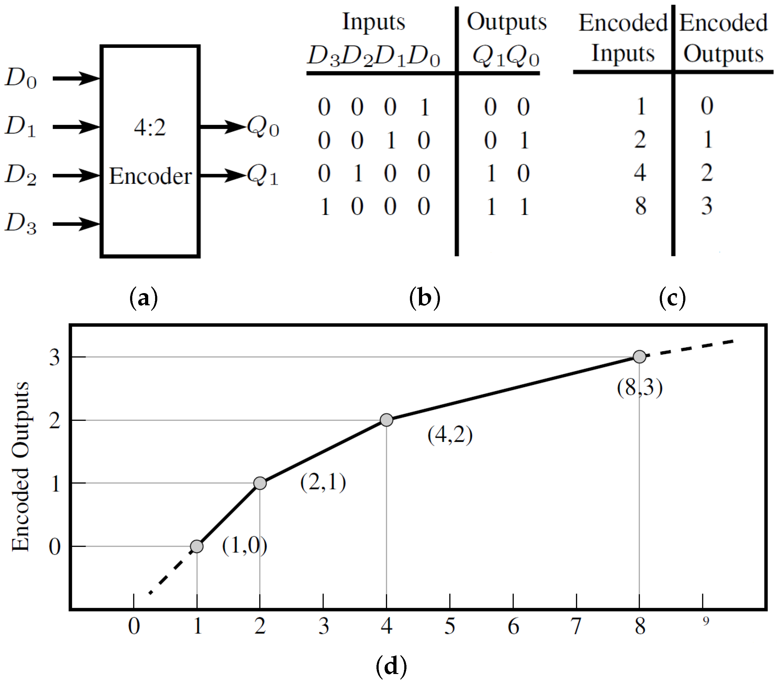
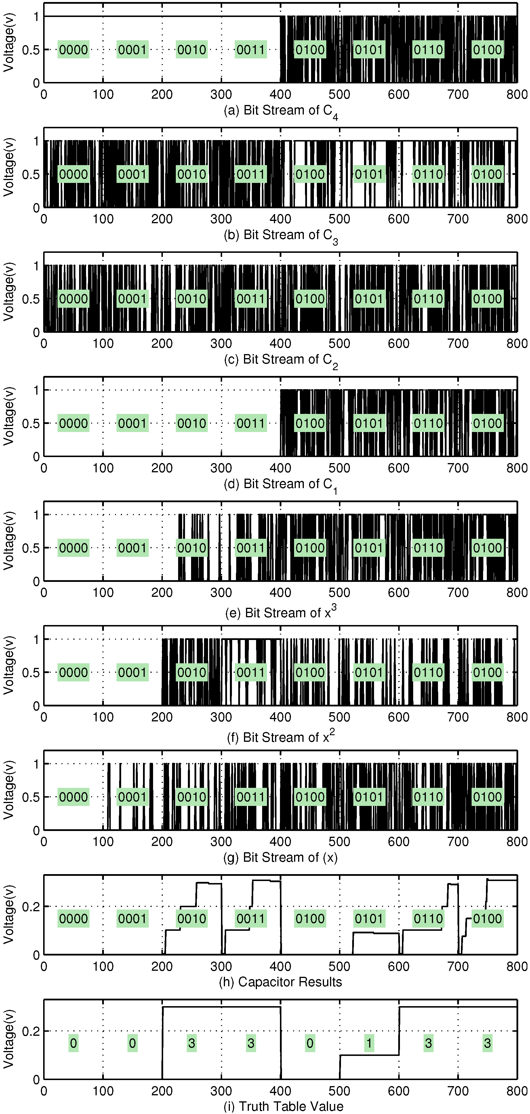
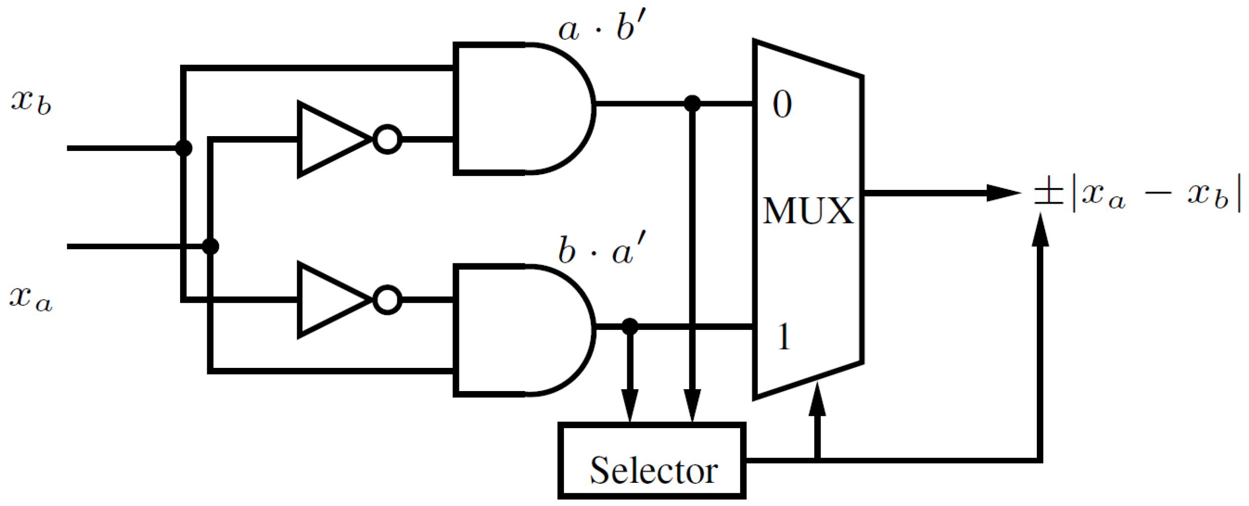
3.1. Algebraically Reinterpreting K-Map

We now interpret the standard Boolean K-map in a different angle. For example, a 4:2 encoder shown in Figure 3a can be represented as a truth-table listed in Figure 3b. If we encode its binary input and output bits as decimal numbers, we obtain a single-input-single-output function as in Figure 3c. Furthermore, such a functional one-to-one mapping can be plotted as a simple algebraic curve shown in Figure 3d. For example, as shown in Figure 3a, when ( D 3 , D 2 , D 1 , D 0 ) = ( 0 , 1 , 0 , 0 ), the output ( Q 1 , Q 0 ) = ( 1 , 0 ) , which can be computed either by looking up the K-map in Figure 3b, or by evaluating the curve at the point ( 4 , 2 ) . This idea can be used to implement a new kind of reconfigurable logic fabric, which has been wildly successful in modern computing due to its low NRE cost. However, the conventional Look-Up Table (LUT), although logically universal, incurs approximately O( 2 N ) of hardware cost for a N-input-1-output logic function due to the number of required reconfiguration memory bits. Our stochastic curve-based logic block can potentially achieve O(N) in hardware cost. This research thrust also involves developing various CAD modules of logic synthesis, LUT placement, and routing algorithms.
Note that both representations in Figure 3a,b are logically equivalent, albeit in totally different forms. Moreover, any given m-input and n-output logic function, with a properly chosen encoding scheme, can be transformed into a well-defined algebraic curve. Therefore, we can recast the problem of logic circuit design into building hardware structure that performs functional evaluation by interpolating algebraic curves. Unfortunately, although Taylor expansion is known to be capable of approximating any form of complex algebraic function by summing power terms calculated at specified points, i.e., f ( x ) = n = 0 N f ( n ) ( x 0 ) n ! ( x - x 0 ) n , where x 0 is constant, directly performing all these constituting operations are quite expensive in CMOS digital hardware. Fortunately, we exploit the quantum-induced Gaussian-like stochastic switching behavior of spin-torque-transfer devices, therefore completely bypassing the aforementioned performance bottlenecks. Specifically, ( x - x 0 ) n = exp ( ln ( x - x 0 ) n ) = exp ( n ln ( x - x 0 ) ) , where n = 0 , 1 , 2 , . Because, the stochastic switching behavior of a MTJ device exhibits a probability density function (P.D.F.) in an exponential form, as discussed in the following subsection, we can bypass both expensive operations exp ( · ) and ln ( · ) .

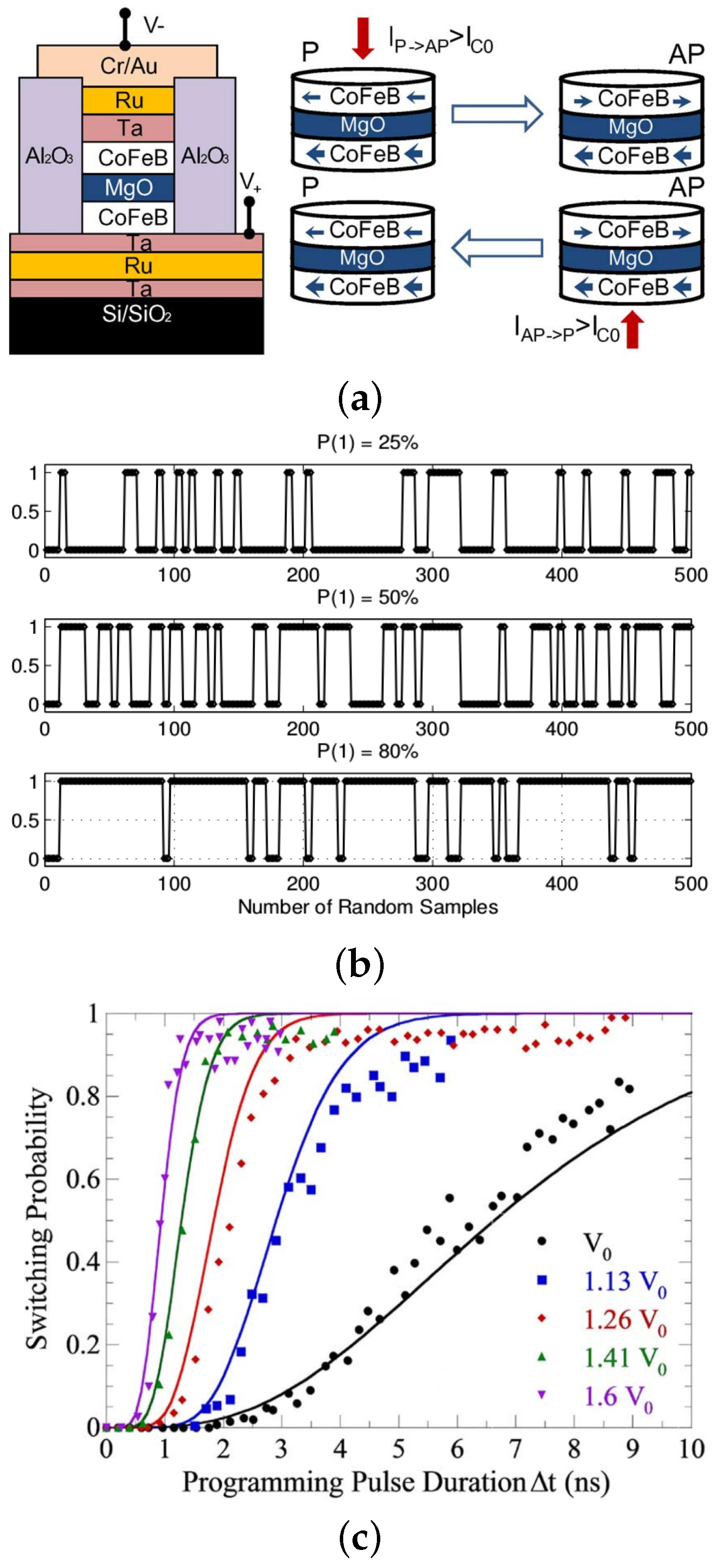
3.2. Stochastic Switching with MTJ Devices

Emerging spintronic devices can exhibit complex switching behaviors due to the shifting of their intrinsic magnetic moment (spin) of electrons. For example, in MgO-based magnetic tunneling junctions (MTJs) (depicted in Figure 4a) [23], the switching characteristic of their spin-torque switching is highly stochastic and exhibits a well-defined probability as shown in Figure 4b. Several recent studies have discovered that MTJ’s switching probability, P sw , mainly depends on its intrinsic switching current and a thermal stability parameter (Δ), where the Δ = E u / k B T , E u , k B , and T are uni-axial magnetic anisotropy energy, Boltzmann’s constant, and temperature, respectively. In fact, if assuming the initial state of MTJ is parallel and one bit current information is stored in the MTJ, a write current signal I w applied during time t can exhibit a switching probability defined by p w = 1 - exp ( - t / τ p ) , where τ p is the switching time constant. According to [24], its switching probability P sw can be controlled by changing the applied pulse width and amplitude [25] and can be concisely formulated as P sw ( I ) = 1 - exp ( - t τ p exp ( - Δ ( 1 - I / I c 0 ) ) ) , where I c 0 is the critical switching current at 0 K. Therefore, by controlling the critical current I c and the duration of applied pulse current τ p , one can accurately predict the switching probability of a given MTJ device. In Figure 4c, we have plotted some of our experimental and analytical results of switching probability vs. the pulse duration for different voltages [6,22].
In Figure 5, we present our design of a reconfigurable random sample generator with two MTJ devices. Its key idea is to exploit the stochastic switching of a MTJ device at different input currents under a fixed pulse duration. Compared with the conventional LFSR-based random number generation, such a MTJ-based methodology can provide not only true randomness but also ultra-fast generation speed. In its configuration mode (Figure 5a), depending on the precomputed STL weights, the MTJ-based memristor is configured with its resistance set in order to produce the required current. The probability of spin-torque switching model P sw ( I ) according to the current I is given by
P sw ( I ) = 1 - exp ( - τ p exp ( - Δ ( 1 - I / I c 0 ) ) )
where I is applied current, τ p is the pulse width normalized by the attempt time. In its operation mode (Figure 5b), depending on the applied logic input, a “0” or “1” value is first written into the right MTJ. Subsequently, a stochastic reading current will be used to perform a read operation on the right MTJ device. The logic output values, i.e., the random samples, are completely determined by both the logic value stored and the reading success probability, which in turn is determined by the magnitude of the reading current I. Note that, by controlling the reading current I and fixing I c 0 , Δ, and τ p , we can match a specific logic weight with a predefined probability value. Finally, the magnitude of reading current I is determined by the reading voltage that is controlled by the resistance of the left MTJ device. The sensing circuit is based on previous MTJ-based true random generator scheme. The analog sensing comparator is used to generate bit stream with an appropriate reference voltage. This analog sensing comparator can be replaced by one or more integrated CMOS inverter to decrease the occupies area on chip [26]. The simulation results from recent fabrication chip test provides sufficient statistical accuracy with negligible device degradation. The distribution of the comparator output voltage typically needs to stay within 50 % ± 1 % to pass the NIST frequency test. Paper [26] utilizes comparator at output, resulting in bimodal abrupt distribution of output voltage along 1000 cycles.

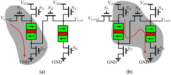
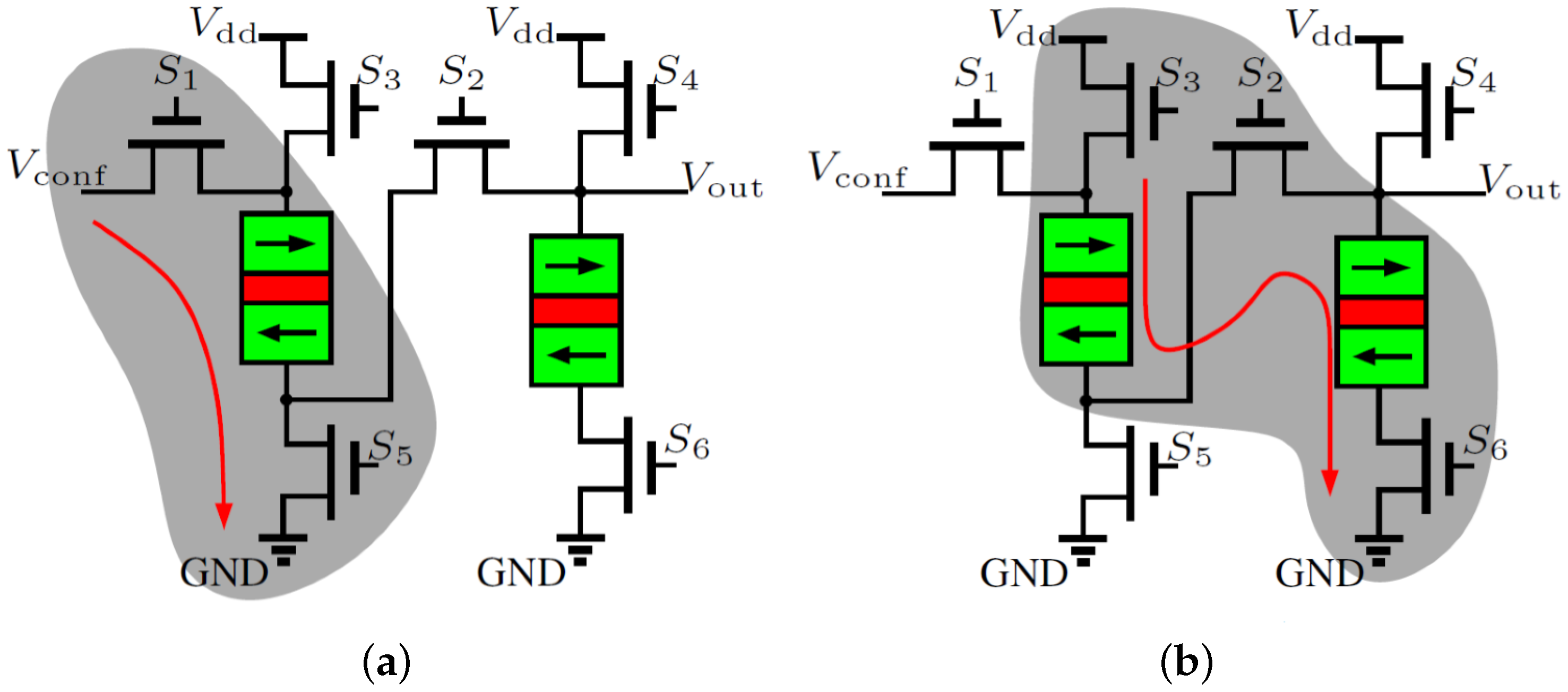
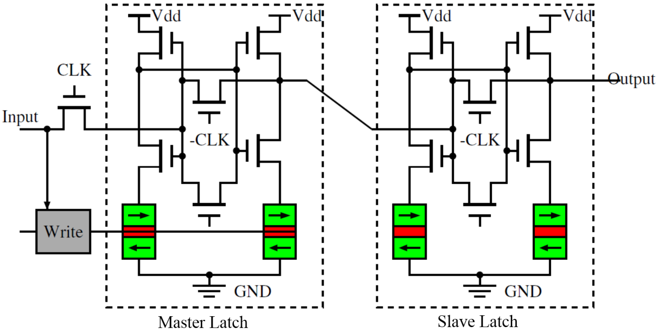
3.3. Detailed Circuit Design of SLB

Figure 6 depicts one possible circuit architecture of stochastic-based logic block (SLB). Specifically, each MTJ device implements an exponential Random variable, whose random samples will subject to simple AND or OR logic operations with CMOS gates. In general, the number of required Taylor terms equals to the the number of needed STT devices, with specific Taylor coefficients are configured with setting different V i . As shown in Figure 6b, each Stochastic-Based Lookup Table (SLB) exploits multiple streams of carefully controlled random bits, instead of deterministic Boolean algebra used in a conventional FPGA technology to accomplish reconfigurable logic operations. As depicted in Figure 6, the key element of a typical N-input STL circuit consists of N controllable random sample generators, each of which corresponds to one logic input. Each random bit generator is implemented with two MTJ devices, where one MTJ device emits random bits with certain probability determined by the other MTJ device. The detailed circuit design of each random sample generator is also shown in Figure 6c. Note that our design of a reconfigurable random sample generator contains two MTJ devices and their detailed operations are discussed in Subsection 3.2. Subsequently, all these N streams of random bits will be aggregated with simple analog circuits and fed into a simple capacitive voltage integrator. The final logic output value will be computed by comparing the integrated value with a predetermined voltage reference V ref = T .
Given the circuit design of our stochastic-based logic block (SLB), we can perform the detailed mixed-mode HSPICE circuit simulation using the model of MTJ devices in Cadence from [21]. The specific device parameters include: I d 0 = 0 . 1 nA, n = 2 , the critical current I c 0 s = 50 μ A, the characteristic resistance R P = 1 KΩ, R AP = 2 KΩ, E / k B T = 60 , the relaxation time t relax = 50 ps, and the attempt time t = 1 ns. To illustrate, in Figure 7, we plotted the HSPICE simulations results from a STL circuit that implements F = A + B C . The first four subfigures, Figure 7a–d present the random signals generated from four constant coefficients c 0 , c 1 , c 2 , and c 3 . Similarly, three additional random sample streams, Figure 7e–g, represent the three power terms. The aggregated and integrated random signals are plotted in Figure 7h. Finally, after thresholding, the resulting logic outputs are presented in the Figure 7i. Note that each of these nine subfigures comprises of eight input epochs and all logic values corresponding to these input epochs are printed in green squares.
Two circuit blocks are essential: log-amplifier block and analog-to-stochastic converter block. The log-amplifier naturally fits an input current into the exponential form of the Taylor series, so that the input analog current I i n and the output voltage V out satisfy V out = - m × V T × ln ( I in I s ) , where m is correction factor, I s is the theoretical reverse-saturation current, and V T is the temperature equivalent voltage. In the stochastic converter block, when the logarithmic voltage is applied to a MTJ device, the resulting current for controlling stochastic switching follows I w = V dd - V bias R MTJ - m × k B × T × ln ( I in / I s ) q × R MTJ . Therefore, ln ( P w ¯ ) = β ln ( I in I s ) + α ( I c 0 s - V dd - V bias R MTJ ) , where β = α m k B T q R MTJ . One rudimentary stochastic subsection unit is presented in Figure 8. More efficient circuit designs are to be explored.
As shown in Figure 6a, a standard logic block also contains flip-flops for supporting sequential circuits. We developed a simple MTJ-CMOS circuit design for a master-slave flipflop. As shown in Figure 9, our design is largely inspired by the 6T-SRAM cell design except replacing the cross-linked feedback cells with four MTJ devices [27]. We believe this design may be further optimized to use fewer devices.
When designing, implementing, and programming a stochastic-based logic block (SLB), four parameters, input number m, output number n, the number of random sample units K, and the number of random samples K per logic epoch, are essential. We now discuss the tradeoff relationship between them. During technology mapping stage, the granularity of a SLB, defined by both m and n, can significantly affect the total number of SLB usage for any given target circuit. Intuitively, increasing the output number n allows each SLB to implement larger logic function. However, when n increases, as shown in Figure 6b, we need larger muxes and higher ADC resolution, both of which consumes more chip area. Furthermore, to meet the accuracy requirement of stochastic-based logic operations, more random sample are often needed, which prolongs the overall stochastic processing time. Note that adding and evaluating more Taylor power terms can also greatly improve the logic precision. But again, this needs more programmable random sample generators, which almost linearly increases the chip area for each SLB. Apparently, how to optimally tradeoff these competing parameters in the application of SPGA remains to be quite challenging and more systematic investigations are needed.

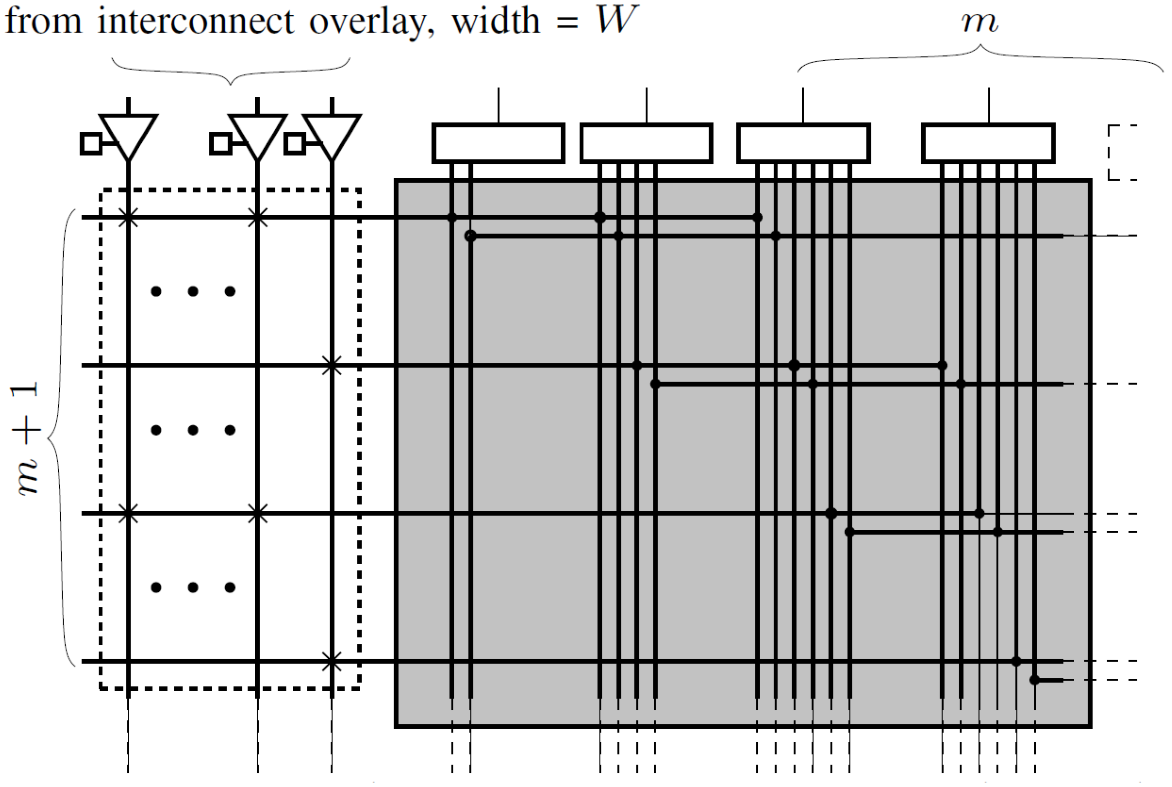
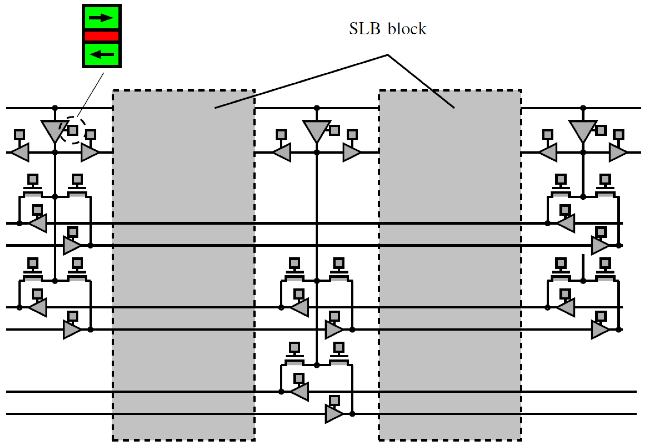
4. Interconnect Architecture

In modern FPGAs, the routing fabric not only contributes the most to the system delay but also consumes most of the chip area [28,29]. To make the situation even worse, the fraction of total delay due to routing in an FPGA is increasing with each process generation [7]. Consequently, an FPGA architect must devise routing architectures that are both fast and area-efficient in order to fully exploit the performance and density potential of deep-submicron technologies. It is known that interconnect segment length can significantly impact the overall performance of an FPGA [30,31], therefore a good mixture of segment lengths is often sought to optimize its overall performance. We took a different approach and developed a new bypassing interconnect for the SPGA. The key idea is to construct long interconnects without passing through heavy switching points and therefore improve delay and power performance without sacrificing routability. Additionally, the more regular structure in bypassing interconnects makes the delay of long interconnects in the SPGA much more predictable than that in a conventional segmented routing architecture, and therefore makes it easier for the CAD software to find the most optimal routes.
As shown in Figure 10, each routing channel comprises only Single and Double segments. Each Single or Double segment consists of two unidirectional wires controlled by two tri-state buffers. Segments can be connected directly to form longer interconnect segments by appropriately setting the states of the tri-state buffers without entering SLB blocks. This helps reducing the parasitic loading along interconnects due to programming overhead. The segments can also be connected through routing blocks to make bends, fan-out, or connect to logic blocks. The number of interconnect segments in each routing channel is denoted by T and the number of routing tracks in each interconnect segment is r.
Connections between the interconnect overlay and a SLB block are made through a structure similar to the conventional Connection Box (CB) as illustrated in Figure 11. For a SLB block with m MUTs on each side, there are m + 1 lines crossing over with the W interconnect segments from the overlay. We define F c as the connecting flexibility of this structure. In Figure 11, F c = 0 . 5 . Note that when the SLB block is configured as a routing block, this connecting structure enhances the routing capability of the routing block which in the conventional island-style FPGA, if a LB is unused, its associated CB will be idle and only add parasitics to the interconnects.

5. CAD Algorithms

To make meaningful FPGA architecture comparison, it is essential that the CAD tools used to place and map circuits into each architecture are of high quality. The routing phase of the SPGA are largely based on the previously published VPR [32]. Unfortunately, the traditional VPR style CAD flow is not totally suitable for the SPGA architecture because the stochastic-based logic block can efficiently provide multiple outputs and the logic and routing resource has to be partitioned before routing stage.

5.1. Logic Synthesis and Technology Mapping Algorithm

Technology mapping for the SPGA architecture needs to be modified in order to consider multiple-output logic block. Note that most standard cell libraries have multiple output cells, e.g., full adders. Similarly, library free technology mappers could use multiple output cells to significantly reduce area of a circuit. Moreover, current FPGAs have multiple output LUTs. We have implemented a simple algorithm Specifically tailored for the SPGA technology that performs a full covering of a circuit by (k, l)-cuts. This algorithm doesn’t stress on achieving the state-of-the-art on mapping. Instead, We implemented a simple greedy algorithm to search for local maxima. The covering is performed from the inputs to the outputs. At each iteration the largest possible (k, l)-cut is chosen, and all (k, l)-cuts with overlapping nodes are eliminated from the solution space. These iterations are repeated until the circuit is fully covered.
Obviously, the algorithm for efficient cut computation is essential for our approach. Typically, computing single output cuts is only considered. In the case of SPGA, because the cost of using multiple-value logic blocks are relatively low, exploring multiple-output-port logic blocks becomes necessary. We adopt the concept of (k, l)-feasible cuts introduced in [33] in our logic synthesis and technology mapping.
Algorithm 1 presents key steps of computing (k, l)-feasible cuts for any given And-Inv-Graph AIG. It starts with enumerating all k-feasible cuts and all l-feasible backcuts on the circuit AIG. Each computed backcut generates a set of (k, l)-cuts. The function combine_kcuts combines the k-feasible cuts of the nodes belonging to the current backcut d.
Algorithm 1 Algorithm of computing (k, l)-feasible cuts.
1:kcuts ← compute_kcuts (AIG, k)
2:lcuts ← compute_lcuts (AIG, l)
3:for each lcut ∈ lcuts do
4:P combine_kcuts (lcuts)
5:for each πP do
6:  klcut ← create_klcut (π, lcut)
7:  if check_and_fix (klcut) then
8:   klcuts.add(klcut)
9:  end if
10:end for
11:end for
12:return klcut

5.2. Placement Algorithm

Our placement software for the S-FPGA is based on a simulated annealing approach with a cost function especially designed to match the routing fabric of the stochastic-based SPGA. For a island-style FPGA, the placement normally uses metrics such as wirelength as well as some measure of the routability and delay. If applying the same methodology to the SPGA, minimizing these metrics will not be able to exploit the configurable logic output and logic granularity of a SLB, which almost certainly results in less efficiency. The placement procedure of the SPGA architecture differs from the island-style FPGA in a fundamental way: its successful routing relies heavily on configuring some SLBs as variable-output logic blocks. To achieve high logic density, the routing resource in a SPGA should be distributed non-uniformly based on the routing demands between each pair of logic blocks. As a result, all SLBs must be configured and positioned as part of the placement process.
Algorithm 2 The placement algorithm of SPGA.
1: p RandomPlacement()
2: T InitialTemperature()
3: g g( A ,p)
4:freeze_count < 50
5:while (ExitCriterion() is FALSE) do
6: changes ← 0
7: trials ← 0
8: c EvaluateCost(g,b)
9:while (InnerLoopCriterion() is FALSE) do
10:  trials ← trials + 1
11:   p new RandomSwap(p)
12:  IncrementalRoute(g( A , p new ), b)
13:   Δ c EvaluateCost(g( A , p new )) −c
14:  if Δ c < 0 /*downhill move*/ then
15:   changes ← changes + 1
16:    p p new
17:    g g( A , p)
18:    c * EvaluateCost(g( A , p new ))
19:  end if
20:  if Δ c > 0 /*uphill move*/ then
21:    r Random(0,1)
22:   if r < e - Δ c T then
23:     s p new
24:     g g( A , p)
25:   end if
26:  end if
27:end while
28: T UpdateTemperature()
29:if c * changes then
30:  freeze_count ← 0
31:end if
32:if c h a n g e s t r i a l s < 0 . 01 then
33:  freeze_count ← freeze_count + 1
34:end if
35:end while
We now describe some of functions referred to in Algorithm 2 in more detail. ExitCriterion ( ) make sure the freeze_count is less than a predetermined number, which is set equal to 50. InnerLoopCriterion ( ) is true if trials < TRIALS and changes < CHANGES . Both constants TRIALS and CHANGES are related to the problem size. We set TRIALS and CHANGES equal to 10 W and 0.01 W, respectively. Given a placement of SLB blocks and the benchmark design, the first step of evaluating the cost is to perform the routing using the Steiner tree algorithm. It is well-known that most Steiner tree problems are NP-complete, i.e., thought to be computationally hard. To simplify our placement algorithm and to combat the intractability, we use a heuristic [34], in which we compute the Euclidean minimum spanning tree to approximate the Euclidean Steiner tree problem. Let ( x i , j , y i , j ) be the cost pair for a SLB block located at ( i , j ) . x i , j be the total number of routed signals along both x- and y-directions above the SLB block ( i , j ) , y i , j be the total number of routed signal turns above the SLB ( i , j ) ,
x ¯ = 1 M N i = 1 M j = 1 N x i , j , y ¯ = 1 M N i = 1 M j = 1 N y i , j
c = 1 M N i = 1 M j = 1 N x i , j 2 - x ¯ 2 + 1 M N i = 1 M j = 1 N y i , j 2 - y ¯ 2
The value of cost c roughly reflects the variance of the demand for routing resource from all SLB blocks. Intuitively, small c means high placement quality in terms of the overall routability.

5.3. Routing Algorithm

To map designs into the SPGA, we modified the VPR router [32,35] to accommodate the differences between the routing architecture of our new stochastic-based SPGA and the island-based architecture. The routing algorithm initially routes one net at a time using the shortest path it can find without considering interconnect segment or logic block pin overuse. Each iteration of the router consists of sequential net rip-up and re-route according to the lowest cost path available. The cost of using a routing resource is a function of its current overuse and any overuse that occurred in prior routing iterations. By gradually increasing the cost of an oversubscribed routing resource, the algorithm forces nets with alternative routes to avoid using that resource, leaving it to the net that most needs it. The main difference between our router and VPR is that we keep track of visited nodes during the breadth-first-search to improve the run time. More details of this routing algorithm can be found in [14].

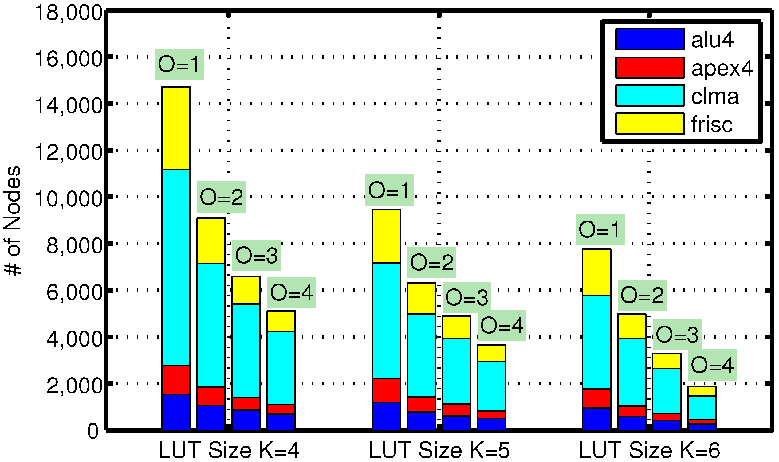
6. Performance Analysis and Comparison
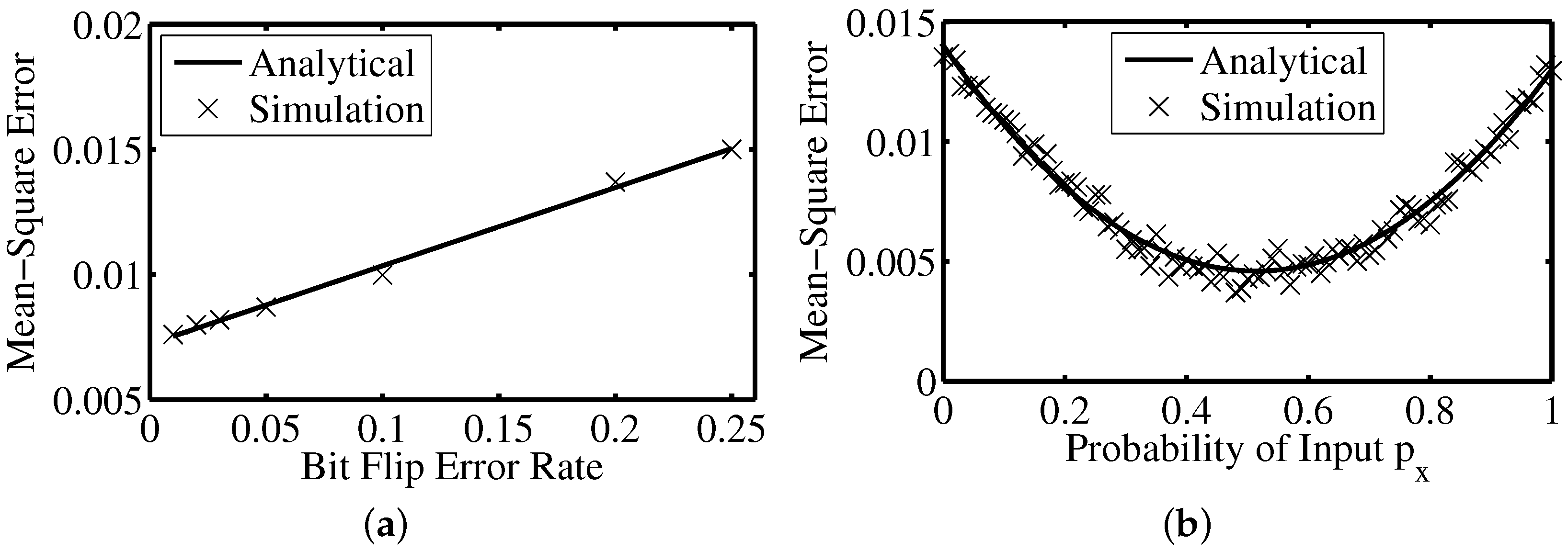
Using the 45 nm CMOS technology node and the In-plane Magnetic Anistrophy (IMA) MTJ Compact model [22], we compare the delay, energy consumption, and transistor count between a baseline island-style FPGA and our stochastic-based spin-programmable gate array (SPGA). Specifically, the MTJ device parameters include: I d 0 = 0 . 1 nA, n = 2 , the critical current I c 0 s = 50 μ A, the characteristic resistance R P = 1 KΩ, R AP = 2 KΩ, E / k B T = 60 , the relaxation time t relax = 50 ps, and the attempt time t = 1 ns. The 45 nm CMOS technology is modelled with the Berkeley Predictive Technology Model (BPTM) [36] for both devices and interconnects.
As in [14], we assume an island-style FPGA as the baseline architecture, referred to henceforth as baseline FPGA, for our performance comparison. It comprises a 2D array of logic blocks (LBs) interconnected via programmable routing. We assume each LB comprises four logic slices, each consisting of two 4-input Lookup Tables (LUTs), two flip-flops (FFs), and programming overhead. The routing fabric comprises horizontal and vertical routing channels each having sets of Single, Double, HEX-3, and HEX-6 interconnect segments. We classify the interconnects into two groups, short, which includes Single and Double FPGA tile width interconnects, and long, which includes HEX-3 and HEX-6 interconnects. The segments can be connected to the inputs and outputs of the LBs via connection boxes and to each other via switch boxes. We assume the MUX-based switch box design described in [37].
For the SPGA architecture, we choose four benchmark circuits to first determine the input number m and output number n for each stochastic-based logic block. The logic synthesis and technology mapping for a given benchmark was conducted with a modified version of the ABC tool based on computing the full covering with (k, l)-cuts as discussed in Subsection 5.1. As shown in Figure 12, with the output number of SLBs increasing, for all four benchmarks, the total number of SLBs will decrease significantly. Not surprisingly, when we increase the input numbers, the total number of SLBs also decreases. However, just as in the case of island-style conventional FPGA, there exists a trade-off between logic block granularity and average net/critical-path delay, in the case of SPGA architecture, there is an additional trade-off between the output number and the total delay performance. This is because, as the output number increases in SLB, the number of total random samples required to compute logic function also increases, therefore prolonging the processing time. In this study, we choose (m, n) = (5, 2) for all measurements.
To accurately measure the chip area of all FPGA architectures we compared, we adopted two different methodologies. For the 2D island-style FPGA, we used the area modelling method at the transistor level, which was first developed in [28,38]. The based FPGA is first decomposed into components including SRAM based LUTs, flip-flops, intra-cluster muxes, inter-cluster routing muxes and switches. The chip area of each of these components is then estimated by counting the total number of minimum-width transistors used. Figure 13 depicts this simple transistor area model. For the SPGA implemented with the hybrid MTJ-CMOS technology, we have to account for its “3D effect”.
We now consider how to measure path delay in a FPGA device. Typically, the total signal path delay in an FPGA device is divided into two components: intra-cluster delay and inter-cluster delay [38], which correspond to the delay due to logic blocks and the routing delay from Interconnect network, respectively. Furthermore, we define average net delay for a placed and routed design as the geometric average of all its pin-to-pin net delays, not including LB delay. As in [14], we first use RC models for the interconnect segments and more delay to optimize the connection and switch box device sizes as well as the number and sizes of the buffers for the HEX-3 and HEX-6 segments for a given FPGA array size in each technology node. We then use a modified version of the VPR delay calculation function to compute net delays.
The delay across a typical stochastic-based logic block, as shown in Figure 14, can be divided into five segments. Table 1 presents our measurements for all these delay segments. The intra-cluster delay contains delay from A C , which is delay from local buffer and routing muxes, and random sample generation module. In the Table 2, the delay of local buffer and routing muxes is calculated with cluster size N = 4, and LUT size (m, n) = (5, 2). By increasing cluster size of N or LUT size (m, n), the total delay due to muxes will increase because more output muxes are needed. However, this delay increase is completely negligible when compared with the delay due to random sample processing. This is because that the stochastic Taylor expansion utilizes random bit streams, the processing delay of A C strongly depends on and grows almost linearly with the number of random bits in each stream. The stochastic multiplication is implemented by fully parallel AND gates, thus, the delay of AND gate C D ( ps ) is added. The large fan-in addition employs large input muxes. The of muxes D E ( ps ) is also determined by the number cluster size N and LUT size K . The delay of the analog integrator is also examined using a high speed module in SPICE. The results are shown in Table 2.
We now compare the performance of our SPGA against three of other FPGA architectures using the 45 nm CMOS technology node and the Perpentidular Magnetic Anistrophy (PMA) MTJ Compact model [22]. In total, we consider three performance metrics: delay, energy consumption, and transistor count or chip area. The first FPGA is a typical 2D island-style architecture implemented with 45 nm CMOS technology. The second work [39] utilizes MTJ device to replace SRAM for constructing LUT. The third architecture is based on the work in [10,40], where a nano crossbar architecture is used to replace the conventional NVFM for high density and lower power consumption. The fourth FPGA is a 3D rFPGA first presented in [41] that utilizes high-density resistive memory (RRAM) to build FPGA components. Different from the existing CMOS-nano hybrid circuits that use crossbars, the proposed rFPGA structures consist of mainly 1T1R structures (1 CMOS transistor is integrated with a two-terminal resistive nanojunction) that can be fabricated using a CMOS-compatible process. Our software tool chain is mostly based on the well-know VPR package from University of Toronto and a modified version of ABC from UC Berkeley. In particular, our power analysis is carried out through the power evaluator, fpgaEvaLP2 [42].
Twelve benchmark circuits from MCNC are used for all measurements and all results are listed in Table 3. Not surprisingly, the conventional FPGA based threshold logic in the 45 nm device technology consumes the highest power mainly because of the routing interconnects and programmable switches. Secondly, the relatively low utilization rate ( 12%) of conventional FPGA logic fabric significantly reduces its efficiency. In comparison, the second architecture [39] MTJ-based SPGA implementation can significantly save power because of using low power MTJ devices for both memory bits and logic computation. However, replacement of SRAM cell by MTJ cell still remain on high usage of routing resource. The third and fourth architecture employ 3D layout to minimize routing resource. Our proposed stochastic-based SPGA achieves the highest energy efficiency. There are several contributing factors. First, our proposed Taylor series approximation method fundamentally reduces the quantity of connections in system level. Second, MTJ devices can be constructed in a 3D metallic structure, therefore drastically reducing the interconnection energy dissipation. Third, MTJ devices can be operated with ultra-low currents for reading and writing procedure (few μ As). Moreover, static power dissipation almost vanishes due to its non-volatile character. Fourth, the analog comparison circuit with the help of ultra-low power MTJ operations can result in very high energy and area efficiency. Fifth, its latch-free architecture does not require any CMOS latch to improve its delay performance. In fact, its delay is mostly determined by the MTJ switching speed and the sample size. Finally, the proposed high output number SLB can drastically reduce the nodes number and delay.

7. Error Analysis

In this section we analysis the robustness of the proposed design, which comes from two major sources: (1) random bit generation through stochastic switching is much more reliable for MTJ devices; and (2) when information is encoded with random bit streams, complicated operations can be converted into much simpler operation that are typically not only cheaper to implement but also much more error-resilient.
In the following, we provide an intuitive explanation of the robustness of our proposed implementation. In our proposed architecture, each signal X is represented as a stochastic bit stream with its expected value E [ X ] = p X . As in a conventional deterministic-based neural network, the value of signal X in our design will also be distorted with errors manifested by flip errors of its random bit stream. Let e denote the bit error vector with an expected value p e , the stochastic signal X thus becomes X * = X e . Mathematically, the expected value of the signal X with its bit flipping errors can be defined as
p X * = E [ X ] = p X + p e ( 1 - 2 p x )
With the standard definition of mean square error (MSE), the difference between the estimated value p ˜ X * and the exact value p X can be written as
E X * = E [ ( p ˜ X * - p X ) 2 ]
In our S-ANN, we assume the estimated value p ˜ X * to be the average of n independent random samples of X * , which is equal to p ˜ X * = 1 / n i = 1 n = X i * . Therefore, the expected value of X * can be written as
E X * = E [ ( p ˜ X * 2 - p X 2 - 2 p X p ˜ X * ) ] = ( p X * - p X ) 2 + p X * ( 1 - p X * ) n
Combing Equations (4) and (6) leads to
E X * = p e 2 ( 1 - 2 p X ) 2 + 1 n [ p X ( 1 - p X ) + p e ( 1 - p e ( 1 - 4 p X ( 1 - p X ) ) ) ]
This clearly shows that the MSE error of X depends on both bit stream probability p X and bit flip error rate p e . With the increasing of bit stream size n, E X * monotonically decreases. Given a sufficiently large n, E X * quickly converges. Also, Equation (7) also reveals that the bit stream probability of p X = 1 / 2 has better error resilience. Guided with the above analysis, we have conducted extensive Monte Carlo simulations with 32 as the bit switch.
Figure 15 presents our simulation results and clearly shows that our stochastic method possesses inherent error resilience. As such, device or circuit errors have much less effect on the expected value of a stochastic bit stream. Specifically, even a portion of a stochastic bit stream (n bits in size) are flipped, their negative effect to the overall expected value will be reduced by n times. More importantly, such an error will be significantly diminished as n increases. Furthermore, bit flipping in a digital circuit tend to be symmetrical, i.e., equal numbers of 0 - to - 1 s or 1 - to - 0 s. As a result, a large portion of bit flipping within a given random bit stream will naturally cancel out, thus posing negligible error on the overall X value [43].
To further validate our proposed proposed design methodology, we now quantitatively consider various error components in our proposed architecture. MTJ Random Number Generation Error ( e m ) forms the first error component of our stochastic synapse circuit. Mitigating MTJ device variations has been the main focus of many researches. Fortunately, our method utilizes MTJ’s probabilistic switching behavior to build up the stochastic computing scheme, therefore quite insensitive to its device variations. A MTJ’s switching probability P sw mainly depends on critical current I c 0 and thermal stability parameter σ, therefore the variation of these two parameters need to be considered. Because the switching probability of a MTJ can be defined as P sw ( I ) = 1 - exp ( - τ p exp ( - Δ ( 1 - I / I c 0 ) ) ) , the l 2 norm least square error of a given switching probability can be written as as e m = 0 n | P sw - P measure | 2 d I n , where the P measure is the measured probability of switching. Using the above error model to analyze the impact of variation of electrical parameter on MTJ device, as shown in Figure 16a, the matching between the model simulation and theoretical results is very high. The paper [26] proposed similar architecture of true random number generator fabricated on the chip. The results experimentally demonstrates true random number generator based on the stochastic switching behavior of MTJ device. The true random number generator based on the stochastic switching behavior of MTJ device enhance the reliability, speed and power consumption to generate the true bit stream.
The random bit fluctuation error ( e r ) is due to the bit flips in a stream. In this paper, since the number of ones in the bit stream will be used to compute the value of stochastic FPGA, the error of bit fluctuations will affect the stochastic FPGA. The bit stream B i with i = 1 , 2 , , n has L length bit stream. The number of ones in a bit stream is converted to a deterministic value T through the integrated circuit. Because T = 1 L i = 0 L B i , the expected value is T e . However, due to the random fluctuation error, the exact output T value is different from the excepted value T e . The random fluctuation e r can therefore be written as e r = | T - T e | T e ( 1 - T e ) L . In this paper, the expected value T e is calculated from the measurements of the output bit stream. The relationship between different probability and different length of random samples is shown in Figure 16b.
Finally, we consider the error due to DW integration. The DW integration determines the number of ones in a given bit stream. According to the experimental work reported in [44], the reliability of a typical domain wall device is excellent. For example, a Co/Ni wire can achieve a 10-year retention time at 150 degrees and 1 × 10 14 times write. In addition, the experiments in [44] have also shown that the domain wall velocity and critical current are not sensitive to external magnetic field or temperature.

8. Conclusions

With the spintronic device technology surging into the mainstream, how to rethink and redesign the existing FPGA architecture is a fascinating yet challenging research problem. This paper is a first step towards capitalizing on the spintronic device technology natively for direct logic computations. Our stochastic-based Spin Programmable Gate Array (SPGA) architecture deviates from the conventional FPGA architecture by directly utilizing the stochastic switching behavior of emerging device technology for Boolean logic computing, while going beyond simply utilizing spintronic devices as an alternative memory technology.

Acknowledgments

This work was supported in part by an ARODURIP grant, N16-22-6056, an NSF BRIGEgrant, ECCS-1342225, and an NSF CCF grant, 1319884.

Author Contributions

Both Yu Bai and Mingjie Lin developed all analytical methods presented in the paper; Yu Bai and Mingjie Lin wrote the paper; illustrations were generated by Yu Bai and Mingjie Lin; simulated and real experimental data was recorded by Yu Bai; analysis of experiments was performed by Yu Bai, Mingjie Lin.

Conflicts of Interest

The authors declare no conflict of interest.

References

  1. Shin, S.; Kim, K.; Kang, S.M. Memristor applications for programmable analog ICs. IEEE Trans. Nanotechnol. 2011, 10, 266–274. [Google Scholar] [CrossRef]
  2. Jo, S.H.; Chang, T.; Ebong, I.; Bhadviya, B.B.; Mazumder, P.; Lu, W. Nanoscale memristor device as synapse in neuromorphic systems. Nano Lett. 2010, 10, 1297–1301. [Google Scholar] [CrossRef] [PubMed]
  3. Bai, Y.; Lin, M. Universal Random Number Generation with Field-Programmable Analog Array and Magnetic Tunneling Junction (MTJ) Devices. In Proceedings of the 2015 IEEE International Conference on Computer and Information Technology; Ubiquitous Computing and Communications; Dependable, Autonomic and Secure Computing; Pervasive Intelligence and Computing (CIT/IUCC/DASC/PICOM), Liverpool, UK, 26–28 October 2015; pp. 1338–1343.
  4. Bai, Y.; Hu, B.; Kuang, W.; Lin, M. Ultra-robust null convention logic circuit with emerging domain wall devices. In Proceedings of the ACM 26th Edition on Great Lakes Symposium on VLSI, Boston, MA, USA, 18–20 May 2016; pp. 251–256.
  5. Wang, P.; Zhang, W.; Joshi, R.; Kanj, R.; Chen, Y. A thermal and process variation aware MTJ switching model and its applications in soft error analysis. In Proceedings of the 2012 IEEE/ACM International Conference on Computer-Aided Design (ICCAD), San Jose, CA, USA, 5–8 November 2012; pp. 720–727.
  6. Onizawa, N.; Katagiri, D.; Gross, W.; Hanyu, T. Analog-to-stochastic converter using magnetic-tunnel junction devices. In Proceedings of the 2014 IEEE/ACM International Symposium on Nanoscale Architectures (NANOARCH), Paris, France, 8–10 July 2014; pp. 59–64.
  7. Lin, M.; El Gamal, A.; Lu, Y.C.; Wong, S. Performance benefits of monolithically stacked 3D-FPGA. In Proceedings of the 2006 ACM/SIGDA Tenth International Symposium on Field-Programmable Gate Arrays, Monterey, CA, USA, 24–26 February 2006; pp. 113–122.
  8. Chen, A. Accessibility of nano-crossbar arrays of resistive switching devices. In Proceedings of the 2011 11th IEEE Conference on Nanotechnology (IEEE-NANO), Portland, OR, USA, 15–18 August 2011; pp. 1767–1771.
  9. Cong, J.; Xiao, B. mrFPGA: A novel FPGA architecture with memristor-based reconfiguration. In Proceedings of the 2011 IEEE/ACM International Symposium on Nanoscale Architectures (NANOARCH), San Diego, CA, USA, 8–9 June 2011; pp. 1–8.
  10. Tanachutiwat, S.; Liu, M.; Wang, W. FPGA Based on Integration of CMOS and RRAM. IEEE Trans. Very Large Scale Integr. (VLSI) Syst. 2011, 19, 2023–2032. [Google Scholar] [CrossRef]
  11. Ebong, I.; Mazumder, P. Self-controlled writing and erasing in a memristor crossbar memory. IEEE Trans. Nanotechnol. 2011, 10, 1454–1463. [Google Scholar] [CrossRef]
  12. Nandha Kumar, T.; Almurib, H.; Lombardi, F. On the operational features and performance of a memristor-based cell for a LUT of an FPGA. In Proceedings of the 2013 13th IEEE Conference on Nanotechnology (IEEE-NANO), Beijing, China, 5–8 August 2013; pp. 71–76.
  13. Ho, Y.; Huang, G.; Li, P. Dynamical properties and design analysis for nonvolatile memristor memories. IEEE Trans. Circuits Syst. I Regul. Pap. 2011, 58, 724–736. [Google Scholar] [CrossRef]
  14. Lin, M.; El Gamal, A. A routing fabric for monolithically stacked 3D-FPGA. In Proceedings of the 2007 ACM/SIGDA 15th International Symposium on Field Programmable Gate Arrays, FPGA ’07, Monterey, CA, USA, 18–20 February 2007; ACM: New York, NY, USA, 2007; pp. 3–12. [Google Scholar]
  15. Dehon, A. Nanowire-based programmable architectures. J. Emerg. Technol. Comput. Syst. 2005, 1, 109–162. [Google Scholar] [CrossRef]
  16. Kuon, I.; Rose, J. Measuring the gap between FPGAs and ASICs. In Proceedings of the 2006 ACM/SIGDA Tenth International Symposium on Field-Programmable Gate Arrays, Monterey, CA, USA, 24–26 February 2006; pp. 21–30.
  17. Actel, Inc. Automotive ProASIC3 Flash Family FPGAs Datasheet; Actel. Inc.: Dover, NJ, USA, 2007. [Google Scholar]
  18. Xilinx. Virtex-II Pro / Virtex-II Pro X Complete Data Sheet (All Four Modules); PXilinx Inc.: San Jose, CA, USA, 2007. [Google Scholar]
  19. Lewis, D.; Ahmed, E.; Baeckler, G.; Betz, V.; Bourgeault, M.; Cashman, D.; Galloway, D.; Hutton, M.; Lane, C.; Lee, A.; et al. The Stratix II logic and routing architecture. In Proceedings of the 2005 ACM/SIGDA 13th International Symposium on Field-Programmable Gate Arrays, Monterey, CA, USA, 20–22 February 2005; pp. 14–20.
  20. Ahmed, E.; Rose, J. The effect of LUT and cluster size on deep-submicron FPGA performance and density. In Proceedings of the 2000 ACM/SIGDA Eighth International Symposium on Field Programmable Gate Arrays, Monterey, CA, USA, 9–11 February 2000.
  21. Zhang, Y.; Zhao, W.; Lakys, Y.; Klein, J.O.; Kim, J.V.; Ravelosona, D.; Chappert, C. Compact modeling of perpendicular-anisotropy CoFeB/MgO magnetic tunnel junctions. IEEE Trans. Electron Dev. 2012, 59, 819–826. [Google Scholar] [CrossRef]
  22. Vincent, A.; Locatelli, N.; Klein, J.O.; Zhao, W.; Galdin-Retailleau, S.; Querlioz, D. Analytical macrospin modeling of the stochastic switching time of spin-transfer torque devices. IEEE Trans. Electron Dev. 2015, 62, 164–170. [Google Scholar] [CrossRef]
  23. Zhu, J.G.J.; Park, C. Magnetic tunnel junctions. Mater. Today 2006, 9, 36–45. [Google Scholar] [CrossRef]
  24. Yagami, K.; Tulapurkar, A.; Fukushima, A.; Suzuki, Y. Inspection of intrinsic critical currents for spin-transfer magnetization switching. IEEE Trans. Magnet. 2005, 41, 2615–2617. [Google Scholar] [CrossRef]
  25. Fukushima, A.; Seki, T.; Yakushiji, K.; Kubota, H.; Imamura, H.; Yuasa, S.; Ando, K. Spin dice: A scalable truly random number generator based on spintronics. Appl. Phys. Express 2014, 7, 083001. [Google Scholar] [CrossRef]
  26. Balatti, S.; Ambrogio, S.; Carboni, R.; Milo, V.; Wang, Z.; Calderoni, A.; Ramaswamy, N.; Ielmini, D. Physical unbiased generation of random numbers with coupled resistive switching devices. IEEE Trans. Electron Dev. 2016, 63, 2029–2035. [Google Scholar] [CrossRef]
  27. Zhao, W.; Belhaire, E.; Javerliac, V.; Chappert, C.; Dieny, B. A non-volatile flip-flop in magnetic FPGA chip. In Proceedings of the International Conference on Design and Test of Integrated Systems in Nanoscale Technology, DTIS 2006, La Marsa, Tunisia, 5–7 September 2006; pp. 323–326.
  28. Betz, V.; Rose, J. FPGA routing architecture: Segmentation and buffering to optimize speed and density. In Proceedings of the 1999 ACM/SIGDA Seventh International Symposium on Field-Programmable Gate Arrays, Monterey, CA, USA, 21–23 February 1999; pp. 59–68.
  29. DeHon, A. Balancing interconnect and computation in a reconfigurable computing array. In Proceedings of the 1999 ACM/SIGDA Seventh International Symposium on Field-Programmable Gate Arrays, Monterey, CA, USA, 21–23 February 1999.
  30. Ciccarelli, L.; Loparco, D.; Innocenti, M.; Lodi, A.; Mucci, C.; Rolandi, P. A low-power routing architecture optimized for deep sub-micron FPGAs. In Proceedings of the 2006 IEEE Custom Integrated Circuits, San Jose, CA, USA, 10–13 September 2006; pp. 309–312.
  31. Pedram, M.; Nobandegani, B.; Preas, B. Design and analysis of segmented routing channels for row-based FPGAs. IEEE Trans. Comput. Aided Des. Integr. Circuits Syst. 1994, 13, 1470–1479. [Google Scholar] [CrossRef]
  32. Betz, V.; Rose, J. VPR: A new packing, placement and routing tool for FPGA research. In Proceedings of the 7th International Workshop on Field-Programmable Logic and Applications, London, UK, 1–3 September 1997; pp. 213–222.
  33. Martinello, O., Jr.; Marques, F.S.; Ribas, R.P.; Reis, A.I. KL-cuts: A new approach for logic synthesis targeting multiple output blocks. In Proceedings of the Conference on Design, Automation and Test in Europe, DATE ’10, Dresden, Germany, 8–12 March 2010; European Design and Automation Association: Leuven, Belgium, 2010; pp. 777–782. [Google Scholar]
  34. Kahng, A.; Robins, G. A new class of iterative Steiner tree heuristics with good performance. IEEE Trans. Comput. Aided Des. Integr. Circuits Syst. 1992, 11, 893–902. [Google Scholar] [CrossRef]
  35. Ebeling, C.; McMurchie, L.; Hauck, S.; Burns, S. Placement and routing tools for the Triptych FPGA. IEEE Trans. Very Large Scale Integr. Syst. 1995, 3, 473–482. [Google Scholar] [CrossRef]
  36. Cao, Y.; Sato, T.; Orshansky, M.; Sylvester, D.; Hu, C. New paradigm of predictive MOSFET and interconnect modeling for early circuit simulation. In Proceedings of the IEEE Custom Integrated Circuits Conference (CICC), Orlando, FL, USA, 21–24 May 2000; pp. 201–204.
  37. Lemieux, G.; Lewis, D. Circuit design of routing switches. In Proceedings of the 2002 ACM/SIGDA Tenth International Symposium on Field-Programmable Gate Arrays, Monterey, CA, USA, 24–26 February 2002; pp. 19–28.
  38. Ahmed, E.; Rose, J. The effect of LUT and cluster size on deep-submicron FPGA performance and density. IEEE Trans. Very Large Scale Integr. (VLSI) Syst. 2004, 12, 288–298. [Google Scholar] [CrossRef]
  39. Zhao, W.; Belhaire, E.; Chappert, C.; Mazoyer, P. Spin transfer torque (STT)-MRAM-based runtime reconfiguration FPGA circuit. ACM Trans. Embed. Comput. Syst. (TECS) 2009, 14, 2–9. [Google Scholar] [CrossRef]
  40. Abid, Z.; Liu, M.; Wang, W. 3D integration of CMOL structures for FPGA applications. IEEE Trans. Comput. 2011, 60, 463–471. [Google Scholar] [CrossRef]
  41. Liu, M.; Wang, W. rFGA: CMOS-nano hybrid FPGA using RRAM components. In Proceedings of the 2013 IEEE/ACM International Symposium on Nanoscale Architectures (NANOARCH), Anaheim, CA, USA, 12–13 June 2008; pp. 93–98.
  42. Li, F.; Lin, Y.; He, L.; Chen, D.; Cong, J. Power modeling and characteristics of field programmable gate arrays. IEEE Trans. Comput. Aided Des. Integr. Circuits Syst. 2005, 24, 1712–1724. [Google Scholar]
  43. Li, F.; Lin, Y.; He, L.; Chen, D.; Cong, J. Behavior of stochastic circuits under severe error conditions. IT Inf. Technol. 2014, 4, 182–191. [Google Scholar]
  44. Fukami, S.; Yamanouchi, M.; Koyama, T.; Ueda, K.; Yoshimura, Y.; Kim, K.-J.; Chiba, D.; Honjo, H.; Sakimura, N.; Nebashi, R.; et al. High-speed and reliable domain wall motion device: Material design for embedded memory and logic application. In Proceedings of the 2012 Symposium on VLSI Technology (VLSIT), Honolulu, HI, USA, 12–14 June 2012; Volume 63, pp. 61–62.
Figure 1. (a) Cross-section of a Magnetic Tunnel Junctions (MTJ)-CMOS hybrid chip; (b) Monolithically stacked 3D-Field Programmable Gate Arrays (FPGA) [7].
Jlpea 06 00015 g001
Figure 2. (a) 2-D Island-style FPGA architecture; (b) Spin-programmable Gate Array (SPGA) architecture with hybrid MTJ-CMOS devices.
Jlpea 06 00015 g002
Figure 3. (a) Logic diagram of a 4:2 encoder; (b) Truth table; (c) Encoded inputs and outputs; (d) Logic curve interpretation.
Jlpea 06 00015 g003
Figure 4. (a) Structure of an MTJ device given from [21]; (b) Our SPICE (Simulation Program with Integrated Circuit Emphasis) simulation results of random signal generation; (c) Experimental and analytical results of switching probability vs. the pulse duration at different voltages [6,22].
Jlpea 06 00015 g004
Figure 5. Circuit design of random bit stream generation. (a) Configuration mode; (b) Operation mode. Devices in gray area are active for each mode. Red curves depict signal directions.
Jlpea 06 00015 g005
Figure 6. (a) Simple conventional LB; (b) Architecture of stochastic-based logic block (SLB); (c) Programmable random bit generator.
Jlpea 06 00015 g006
Figure 7. Mixed-mode circuit simulation results of our stochastic-based logic block.
Jlpea 06 00015 g007
Figure 8. Hardware implementation of stochastic subtraction.
Jlpea 06 00015 g008
Figure 9. Circuit of a MS -register with four MTJ devices.
Jlpea 06 00015 g009
Figure 10. Interconnect overlay and its logic design.
Jlpea 06 00015 g010
Figure 11. Connections between interconnect overlay and a SLB block.
Jlpea 06 00015 g011
Figure 12. The logic synthesis of large fanin and multible fanout Loop-Up table is shown and simulated through logic synthesis tool ABC. The 4 benchmark circuits are taken into consideration. In this Figure, we can see to deceasing trends, one is with Look-Up table size increasing, another is with output increasing. The results show that with the Look-Up table size and output number increasing. The number of nodes in logic network is significantly decreasing. The ratio of decreasing is trending slow, since the small input and output node is decreasing.
Jlpea 06 00015 g012
Figure 13. Layout area measuring model. (a) Conventional transistor layout; (b) 3D MTJ and control transistor layout.
Jlpea 06 00015 g013
Figure 14. Delay breakdown of proposed stochastic-based logic block.
Jlpea 06 00015 g014
Figure 15. (a) The mean square error (MSE) simulation of stochastic bit stream with increasing of bit flip error rate both in analytical and simulation method; (b) The MSE simulation of stochastic bit stream with different probability both in analytical and simulation method [43].
Jlpea 06 00015 g015
Figure 16. (a) Simulation of theoretical and simulated results; (b) Random bit stream error with different bit length.
Jlpea 06 00015 g016
Table 1. Delay of proposed new stochastic FPGA architecture. The CMOS device is using 0 . 18 μ s process.
A B ( ps ) B C ( ps ) C D ( ps ) D E ( ps ) E F ( ps )
301.3305.1250.2522.4478.1
Table 2. Delay of SPGA architecture with 45 nm CMOS technology node.
STT-MRAMProposed
transistor count154 MOS + 32 MTJ6 MOS + 32 MTJ
active power ( μ W )13.43.22
standby power ( μ W )00
Table 3. Benchmark circuit synthesis using propose Look-Up table architecture with large input and output number.
DesignConv. 2D Arch.RRAM FPGA [39]3D CMOS FPGA [10,40]3D rFPGA [41]Proposed SPGA Arch.
# ofAreaDelayPower# ofAreaDelayPower# ofAreaDelayPower# ofAreaDelayPower# ofAreaDelayPower
LUTs ( 10 5 μ m 2 )(ns)(mW)LUTs ( 10 5 μ m 2 )(ns)(mW)LUTs ( 10 5 μ m 2 )(ns)(mW)LUTs ( 10 5 μ m 2 )(ns)(mW)LUTs ( 10 5 μ m 2 )(ns)(mW)
alu45121.377.13625120.8717.5545126.883.6456.25125.863.6446.6631.444.1310.78
apex27061.668.6677060.8818.77557068.34.3862.17066.184.3853.11092.114.3411.22
apex46184.147.3426182.0117.63761820.733.7440.361811.543.7429.81313.184.2212.2
mise35004.627.4251.35002.8817.4247.025006.23.3749.95004.763.3738.4971.984.1110.98
diffeq5263.915.56245262.0515.77195265.013.2425.25264.383.2423.21393.194.2312.36
elliptic1332.3010.7691331.65215813310.685.9670.21337.195.9658.71583.585.3720.6
ex10106121.2414.61136120.7525.610561219.565.9411661211.325.9497.91132.384.8511.31
frisc19051.613.362.719050.824.556.5190511.56.9567.219058.546.9568.31764.334.5830.83
seq7392.648.4657391.8219.5557397.53.74627395.53.7450.21182.414.1511.86
spla4491.3713.38744916.35.6795.44490.7424.3784499.035.6755.71162.394.5111.45
pdc2764.3816.81012762.7718.89627618.47.6910727610.767.6977.51413.225.7515.81
tseng5391.666.96295390.833.48255393.923.5430.15393.893.5429.81082.053.8811.12

