Article

A Sub-Threshold 8T SRAM Macro with 12.29 nW/KB Standby Power and 6.24 pJ/access for Battery-Less IoT SoCs

1
Department of Electrical and Computer Engineering, University of Virginia, Charlottesville, VA 22904, USA
2
Psikick, Charlottesville, VA 22902, USA
*
Author to whom correspondence should be addressed.
J. Low Power Electron. Appl. 2016, 6(2), 8; https://doi.org/10.3390/jlpea6020008
Submission received: 31 December 2015 / Revised: 15 April 2016 / Accepted: 17 May 2016 / Published: 24 May 2016

Abstract

:
We present an ultra-low power (ULP) 1 KB SRAM macro for Internet of Things (IoT) battery-less systems-on-chip (SoCs) operating under varying energy harvesting conditions. The unique combination of features within this array allows battery-less SoCs to retain important information for a significantly longer period of time when energy harvesting conditions are poor. The array uses 8T high-threshold (high-VT) static random access memory (SRAM) cells with word line boosting to eliminate write failures coupled with a read-before-write scheme to address read-disturb in half-selected cells. Due to the reduced on current in high-VT devices, read word line boosting is implemented to improve the drive strength of the read buffer, and to eliminate read failures. Leakage currents through the unselected cells during a read operation is addressed by boosting the footer virtual VSS (VVSS) of the read port to the supply voltage (VDD). To reduce the power consumption of instruction memories in battery-less SoCs, two features were utilized in this array: a read burst mode is used when reading consecutive addresses to reduce the read energy, and instructions with higher percentages of “1” data are defined since reading a “1” is less costly than reading a “0” in 8T cells. The proposed array can operate at a wide range of supply voltages (350–700 mV) and has two ULP modes: standby with retention (1.5 pW/bit) and shutdown without retention (0.13 pW/bit). Aggressive power gating of all peripherals during the standby state reduces the array power consumption down to 12.29 nW/KB at 320 mV with data retention. Compared to previously published 8T arrays, the proposed design provides the lowest standby power. The complete shutdown of the array allows further reduction down to 1.09 nW/KB and is suitable for reducing the power consumption of data memories in battery-less SoCs. The measured results from a commercial 130 nm chip show that the proposed array consumes a minimum of 6.24 pJ/access with a 17.16 nW standby power at 400 mV. The read burst mode allows up to 22% reduction in energy/access at 400 mV.

1. Introduction

The huge drive towards the internet of things (IoT) has led to the development of ultra-low power (ULP) systems-on-chip (SoCs) that are capable of operating on harvested energy [1,2]. The circuits within such SoCs must operate reliably under varying harvesting conditions, and thus their energy and power consumption must be kept at a minimum. One way to guarantee low power and energy consumption is to scale down the supply voltage to the sub-threshold region [3]. However, the reduced on-to-off current ratio (ION/IOFF) and the exponential dependence of the current on the threshold voltage (VT) in the sub-threshold region introduces many challenges especially in ratioed circuits such as the traditional 6 transistor (6T) static random access memory (SRAM) bit-cell. Since conventional non-volatile memories consume higher read and write power than the SRAMs, battery-less SoCs [1,2] rely mainly on SRAMs to hold instructions as well as data, although emerging non-volatile memories are reducing these power numbers. Thus, to ensure that the SoC does not lose its data when harvesting conditions are scarce, the SRAMs must be designed carefully to reduce their power consumption without compromising the integrity of their data.
The increased impact of variation in sub-threshold causes write and half select failures in SRAM arrays, while the reduced ION/IOFF introduces read failures. Many approaches were introduced in the literature to address the different challenges facing SRAMs. A number of alternative bit-cell topologies were used in [4,5,6], including the 8T bit-cell [4] (Figure 1) with decouple read and write ports to improve the stability for sub-threshold operation. Different assist techniques [7,8] were also used to improve read and write stability at lower supply voltages. Half-selected cells sharing a row with a selected bit-cell experience pseudo-read during a write operation and are more vulnerable in sub-threshold. To eliminate half-select instability, new bit-cell topologies [9], banks with only one word per row [5,9], and row read-before-write [10] were proposed.
In this paper, we present a fabricated ULP 1 KB SRAM array designed to minimize the sleep power of arrays in battery-less SoCs. The proposed array was fabricated in a commercial 130 nm process since the main target applications are IoT devices that are not performance-driven and that are usually fabricated in more mature technologies [1,2,11,12]. Newer technology nodes offer higher speeds that are not critical for IoT SoCs, and also suffer from higher leakage and higher cost. The reduction of area from scaling is less beneficial for IoT SoCs that have large analog and radio (RF) components, which do not scale significantly across processes. These factors make the 130 nm process one of the attractive technologies for battery-less IoT devices. The proposed array can be easily expanded to 4 KB with minimal additional circuitry. Table 1 summarizes the different features available within the array. The unique combination of features included in this array addresses all the challenges of sub-threshold SRAM. The array uses high-threshold (high-VT) devices and aggressive power gating to reduce the power consumption. A read burst mode is also implemented to reduce the read energy. An 8T bit-cell and a read-before-write implementation are used to address half-select failures. Read and write assist techniques are introduced to ensure correct read and write functionality in the sub-threshold regime. The array can operate reliably between 350 mV and 700 mV, and can retain data down to 320 mV. Leakage power is minimized at 320 mV to 12.29 nW/KB with data retention, and 1.09 nW/KB without data retention. The resulting design makes use of multiple technology, architecture, and assist methods in a unique combination that optimizes SRAM for the IoT space. To the authors’ best knowledge, the proposed array has the lowest power of any 8T SRAM array in the literature.
The rest of the paper is organized as follows. Section 2 introduces the array structure and motivates the different design decisions. Section 3 shows the chip measurement results from fabricating this array in a commercial 130 nm bulk CMOS process. Finally, Section 4 concludes the paper.

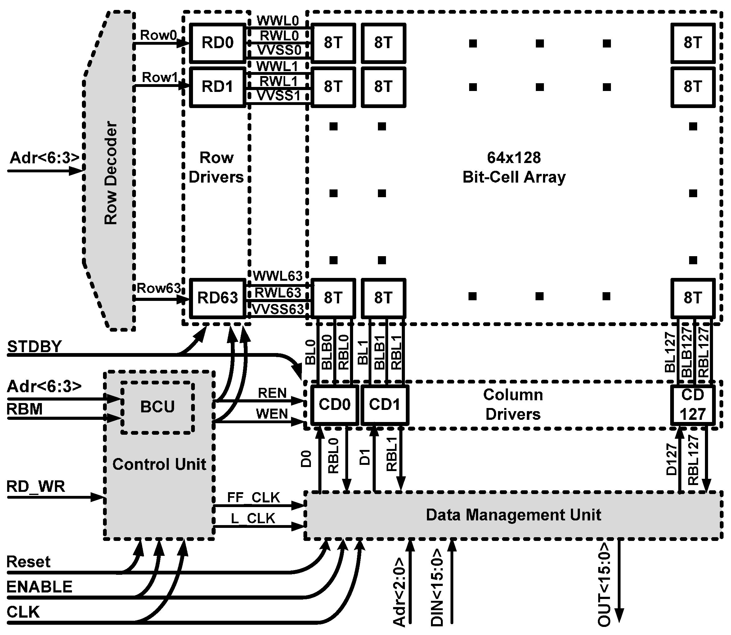
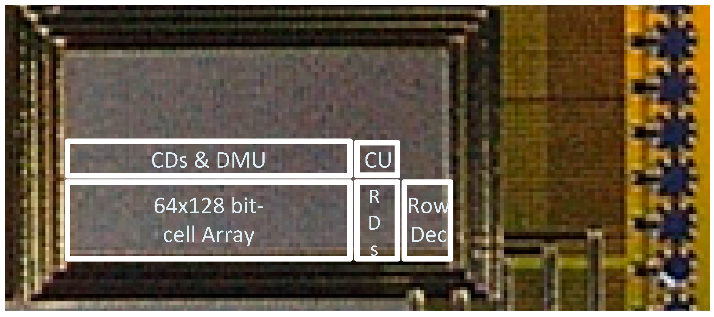
2. Proposed Array Structure
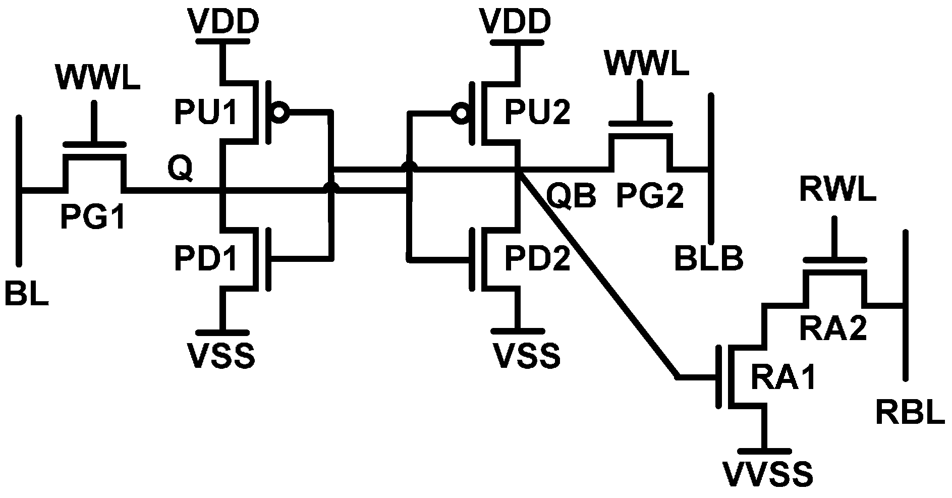
Since the proposed array is designed for battery-less SoCs, it will be used as a building block for three different types of memories: a “hold mostly” memory to save critical information for the longest possible time when energy is scarce, a “read-mostly” memory to hold the program instructions that run on the SoC, and a “read-write” memory to save the data gathered. For the SoCs to support all three types of memories and still operate on harvested energy, the power and energy consumption of these memories must be kept at a minimum. Thus, many of the design decisions and added features aim at reducing the power and energy consumption of the array. Figure 2 shows the overall structure of the array. The 1 KB array consists of 64 × 128 8T bit-cells with row (RDx) and column (CDx) drivers, a row decoder, a read/write control unit with a burst control unit (BCU), and a data management unit (DMU). In the next subsections, we will describe the main features of each unit.
The proposed combination of techniques implemented in this paper can be easily ported into more advanced technologies to reduce the power consumed in the SRAM arrays. However, sub-20 nm Fin Field Effect Transistors (FinFET) bitcells exhibit strong resilience against variation and can reliably write down to 500 mV without assist [13], in large part due to the much lower VTs in those pushed technology nodes. Thus, the degree of assist that needs to be applied to ensure write will be lower than what is required for the 130 nm bitcell presented in this paper (as was shown in [13]). Read-before-write can be implemented in advanced technologies to address half-select failures instead of the dual assist approach presented in [13]. However, the trade-offs between the two approaches need to be assessed for more advanced technologies to determine the more energy-efficient solution (this is outside the scope of the presented work).

2.1. Bit-Cell Array

Due to the challenges of operating the conventional 6T cell at sub-threshold voltages, the bit-cell array is made up of 64 × 128 8T cells (Figure 1) with decoupled read and write ports. High-VT devices are used within the bit-cells to reduce their leakage currents and thus the standby power consumption of the array. However, since high-VT devices have reduced on current, the read and write margins are significantly degraded, necessitating the use of assist techniques to guarantee correct operation. In the following sub-sections, the techniques used to guarantee successful read and write operations are described.

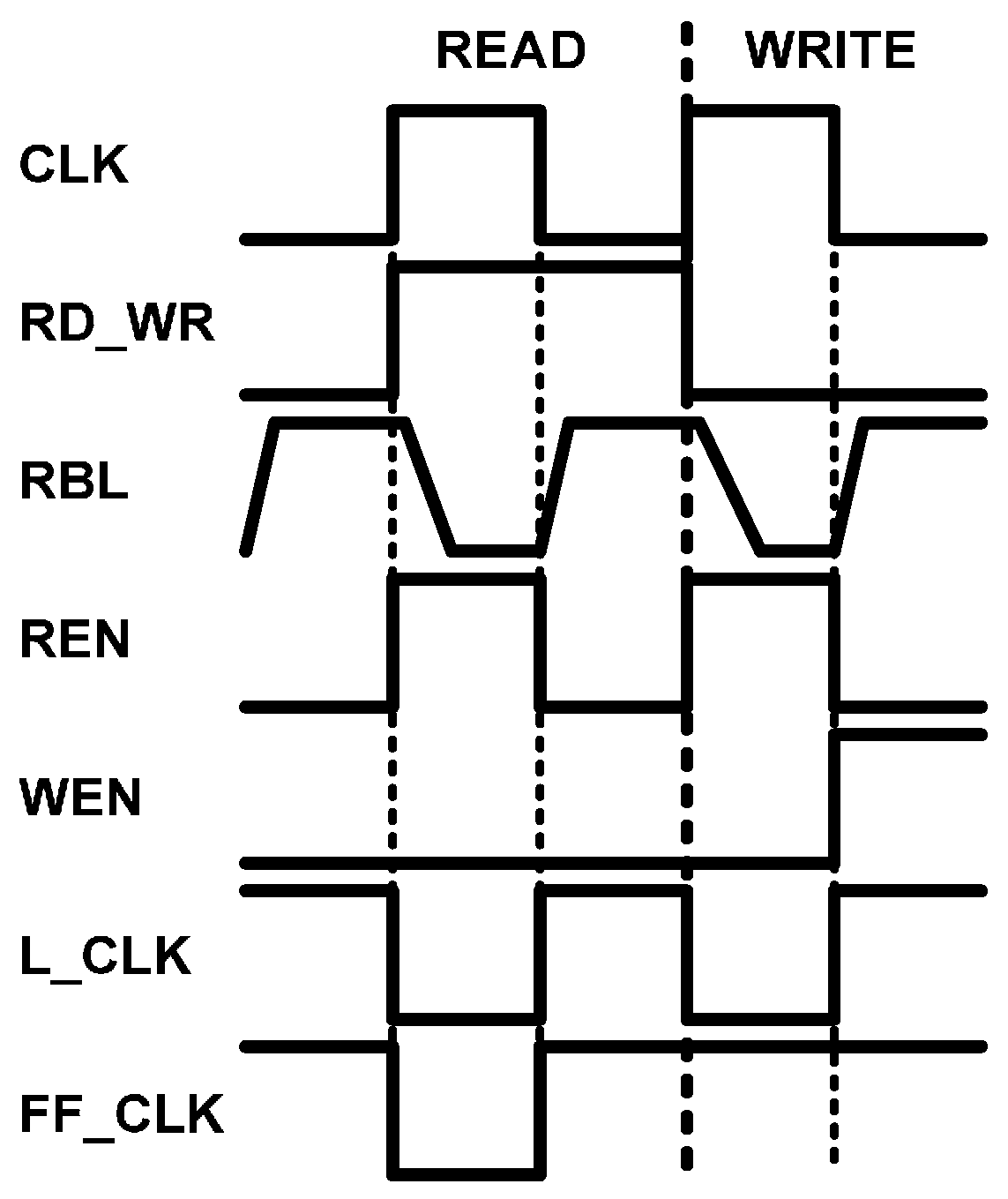
2.1.1. Read Operation

To read the 8T bit-cell, the read bitlines (RBL) are pre-charged by the column drivers before the read wordline (RWL) is asserted by the row driver. Depending on the data within the cell, RBL is either discharged or kept high. However, due to the reduced ION/IOFF in sub-threshold, the off current in the unselected bit-cells on the same RBL might cause an incorrect value to be read out. Thus, the footer voltages (VVSS) of these unselected bit-cells are held high as in [4], and only the accessed bit-cell VVSS is discharged before a read operation. Since the VVSS signal is shared between bit-cells on the same row, its driver must be designed to sink the current from all the bit-cells in a row. Thus, the pull down network of the VVSS driver is overdriven by a charge pump circuit (area overhead <3%) to ensure the VVSS node does not rise [4].
Due to the reduced on-current (ION) of the high-VT devices, the read operation cannot be guaranteed across all process corners/temperatures without the use of an assist technique. Thus, two read assist techniques were considered to improve the read-ability of the 8T cell. In the first approach, RWL is boosted using the charge pump circuit introduced in reference [4]. The charge pump circuit was used instead of a level converter since it does not require an additional high supply voltage, and simulation results showed that it consumes less energy. In the second approach, nominal-VT devices were used in the 2T read port instead of high-VT devices, and no boosting was performed. The two approaches were fabricated and their maximum frequency, leakage power and active power was compared. Table 2 shows the measurement results from the two arrays. Even though the nominal-VT read port improves the read frequency significantly, it also results in more than 2X increase in leakage power and ~4X increase in active read power. Since this array targets IoT applications with relaxed frequency requirements, the RWL boosting approach was chosen instead of the nominal-VT approach to ensure reduced leakage and active power.
To read the value on RBL, our implementation uses a simple output buffer instead of the commonly used sense amplifier to avoid the challenges of operating it at sub-threshold voltages. By limiting the number of bit-cells in a column to 64 and allowing RBL to completely discharge, the output buffer can correctly read the contents of the selected bit-cells. This increases read energy but simplifies timing and increases robustness to variations.
To reduce the read power/energy, the array employs a read burst mode (RBM) feature which makes use of the fact that when RWL is asserted, the complete row experiences a read operation. Thus, when consecutive addresses in the same row should be read, it is enough to perform the read operation once and save the data in latches for the consecutive reads. Accessing the latches will consume significantly lower energy than performing a normal read, thus reducing the overall read energy. The Burst Control Unit (BCU) implementing RBM has a negligible impact on the power (<0.7%), performance (0%) and area (<<1%) of the system, and the potential savings it offers is significantly higher than the cost of implementing it. Section 2.2 describes the implementation of the RBM.
To further reduce the read power/energy of instruction memory (“read-mostly”) arrays in IoT systems, users can make use of the fact that reading a “1” consumes significantly lower power than reading a “0” in 8T SRAM cells [14]. The higher read “0” power is due to the discharging of RBL needed to read a “0”, whereas reading a “1” does not discharge RBL; thus, the only contribution to the read power is the leakage current through unselected cells in the column which is kept at a minimum by boosting the unselected cell VVSS. By designing the instruction set of the IoT processor or by including an encoding scheme that results in more “1” bits than “0” bits in each word, the active power consumption of the array can be significantly reduced. The impact of these techniques on the system area, performance and standby power varies depending on the application. If the IoT processor instruction set is modified, the impact on area, performance and standby power is zero. However this option might not be available to all system designers. On the other hand, the encoding scheme can be widely used but will have an impact on the area, performance and standby power of the system. For example, if the encoding scheme in [15] is used, the area overhead will be ~6% and the standby power will be increased by ~6%. This scheme will have little impact on performance but will allow for a 13% reduction in active power at 400 mV, assuming it can reduce the number of “0” within a word from 50% to 25%. Table 3 below shows the difference in active power consumption of the array (not system) when different percentages of “0”s and “1”s are used within a word. Reducing the number of “0” within a word from 50% to 25% results in 8% and 21% reduction in read power at 350 mV and 400 mV, respectively. Also, since our array relies on read before write to avoid half-select disturbs, the write power is reduced by 9.5% and 17% at 350 mV and 400 mV, respectively.

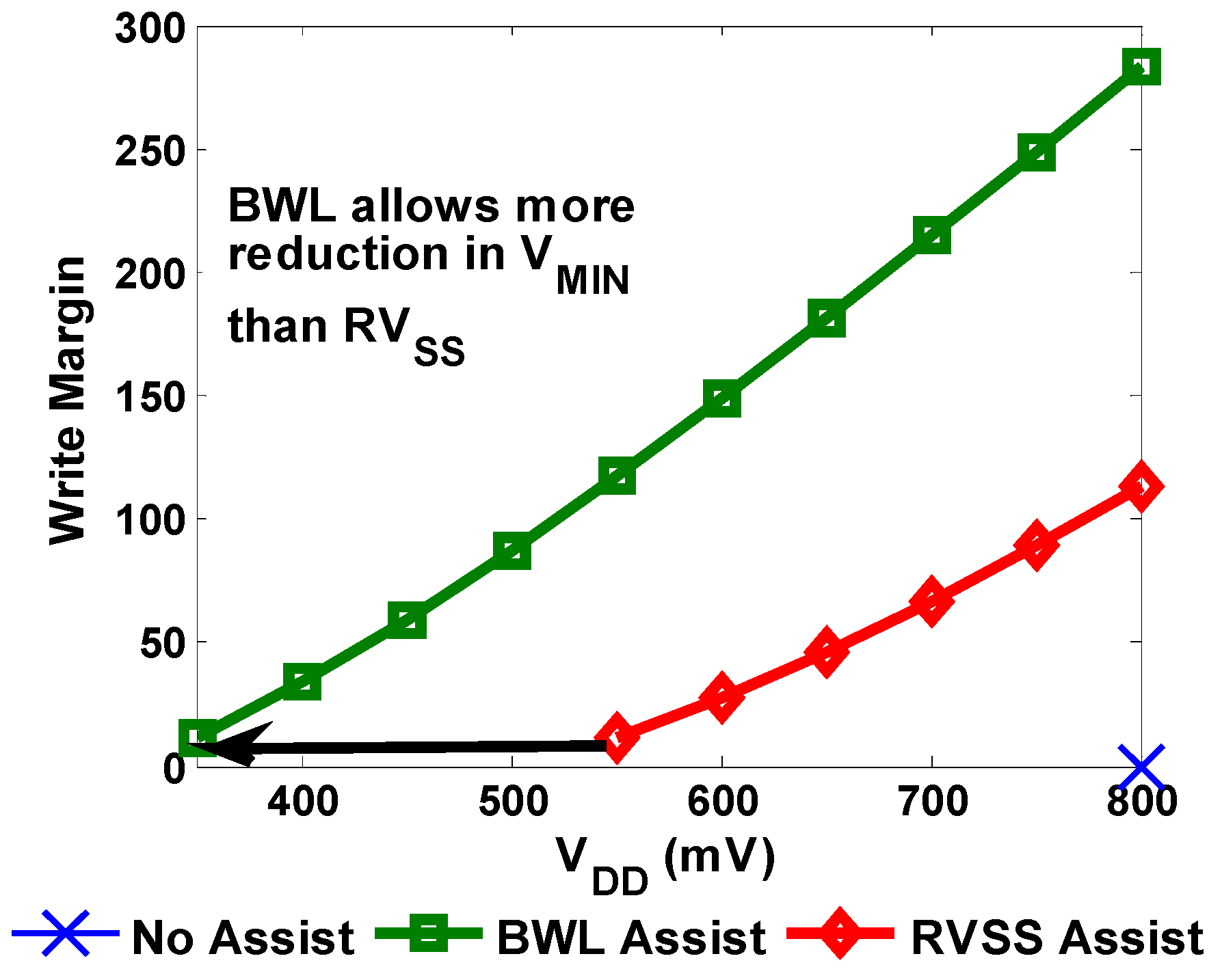
2.1.2. Write Operation

When writing into the 8T bit-cell, the column drivers will set the data on the write bitlines (BL and BLB) before the row driver asserts the write wordline (WWL). Cells sharing the same WWL experience a half-select pseudo-read operation that might corrupt their contents. Thus, we adopted a row read-before-write (RBW) implementation since it provided a good compromise between the added area needed to implement a different bit-cell topology and the added power/energy and area needed to implement the additional logic and drivers for the one-word-per-bank solution. Even though RBW will increase the energy consumed during a write operation, this increase is acceptable for “hold-mostly” and “read-mostly” arrays where the number of writes is limited.
Since high-VT devices are used, the write-ability of the cell is degraded due to the reduced drive strength of the pass transistors. Thus, a write assist technique is needed to guarantee correct write functionality. We evaluated the different write assist techniques to determine the optimal choice for our implementation. Since most battery-less SoCs do not require high performance, the static write margin (WM) can be used as an evaluation metric instead of the critical wordline (WL) pulse width [16]. WM is calculated by sweeping WL, measuring the value at which the contents of the cell switch, and then subtracting that value from VDD [17]. Column-based assist techniques such as Negative BL and Column VDD Lowering were not included in the evaluation due to the large area and energy overhead they will incur when the complete row is written in a row RBW implementation. On the other hand, row-based assist techniques such as WL Boosting and VSS Raising can improve the margins to allow sub-threshold operation with limited impact on area and power. Figure 3 shows the impact of the row-based techniques on the 3σ WM of the 8T bit-cell at the slow-fast (SF) corner (worst write corner) with temperature set to 25 °C. For the same degree of assist applied, WL boosting shows more improvement in WM, and reduces the minimum voltage (write VMIN) at which a write operation can be successfully completed. Thus, the WL boosting assist technique was adopted in this design. To implement this boosting, a charge pump circuit [4] was added within the row driver circuit (RDx) to boost WWL during a write operation.

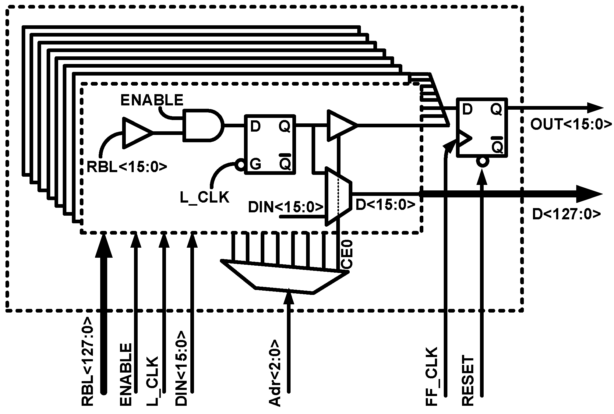
2.2. Control and Data Management Units

The control unit is responsible for reading the inputs to the array, determining the correct mode of operation, and generating the appropriate read, write, and control signals. It takes three inputs: active mode (ENABLE), read/write (RD_WR) and read burst mode enable (RBM), and generates four output signals to control the array: read enable (REN), write enable (WEN), latch clock (L_CLK), and output register clock (FF_CLK). In active mode (ENABLE = 1), the control unit is ready to read/write data into the SRAM array. When RD_WR is asserted, data is read out of the array. First, the control unit drives REN high while keeping WEN low. REN then signals the row drivers to set RWL and VVSS of each row to the appropriate values. At the end of the read cycle, the control unit drives L_CLK high to provide the latching edge for the latches in the DMU. These latches are used to hold the read data to be used when read burst mode is enabled (RBM = 1) or when a write operation should follow the read in the RBW implementation. Finally, FF_CLK is asserted to provide the edge for the output registers.
The read operation is always performed on the high clock phase and takes only half a clock cycle to complete. Thus, the data is available in the latches by the end of the high clock phase. If a write operation is requested (RD_WR = 0), a read is first performed during the high clock phase but FF_CLK is not toggled. At the falling edge of the clock, the control unit asserts WEN which then controls the row and column drivers to set WWL and BL/BLB to the appropriate values.
When RBM is enabled, the BCU within the main controller will keep track of the addresses being accessed and the RD_WR signal. Once two consecutive addresses in the same row are read, the BCU informs the control unit that the data is already available within the latches, thus REN and L_CLK are not toggled.
The DMU shown in Figure 4 manages the data flow in the array. It contains the read output buffer, the data latches, the output registers and the logic required to choose between the input data and the latch data for the write operation. The DMU takes as input the read bitlines (RBL<127:0>), the input data (DIN<15:0>), the column address bits (ADR<2:0>), L_CLK and FF_CLK, and outputs the data read from the array (OUT<15:0>) and the data for the write drivers (D<127:0>).
Figure 5 shows the timing diagram of a read operation followed by a write operation, assuming the array is in the active mode. RBLs are pre-charged during the low phase of the clock (CLK). If the RD_WR signal is high at the rising edge of CLK, REN is driven high to start the read operation. The latch clock signal—L_CLK—is held low until the end of the read operation (signaled by REN going low) where it is toggled high to enable the data latches to save. Based on the column address, one of the eight tristate buffers in the DMU is enabled and passes the data to the rising edge-triggered output registers controlled by FF_CLK. FF_CLK is driven low at the start of the read operation (REN = 1) and high at the end (REN = 0). When the RD_WR signal is low at the rising CLK edge, a write operation is performed. The write operation starts with a read on the low CLK phase (REN = 1 and L_CLK = 0). FF_CLK is not toggled since this data does not need to appear at the output. Once the row data is available (falling CLK edge), the multiplexers in the DMU choose between the latch data and the input data (DIN<15:0>) based on the column address, and then feed the result (D<127:0>) into the column drivers. Next, the WEN signal is asserted, to enable WWL and drive BL/BL to complete the write operation.

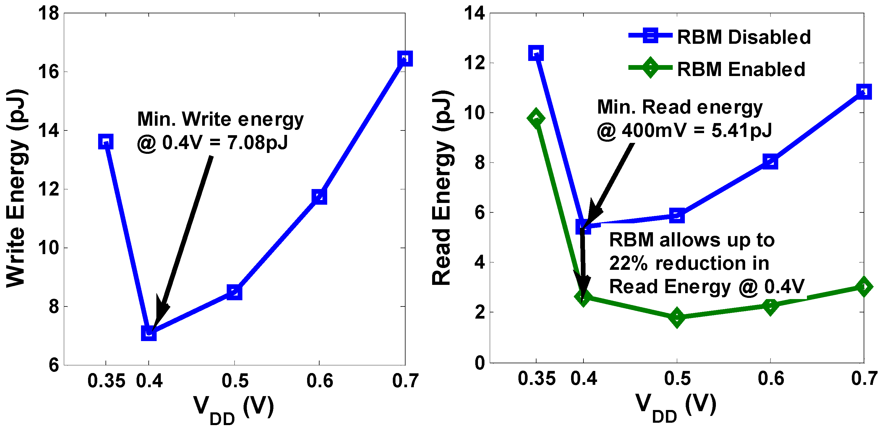
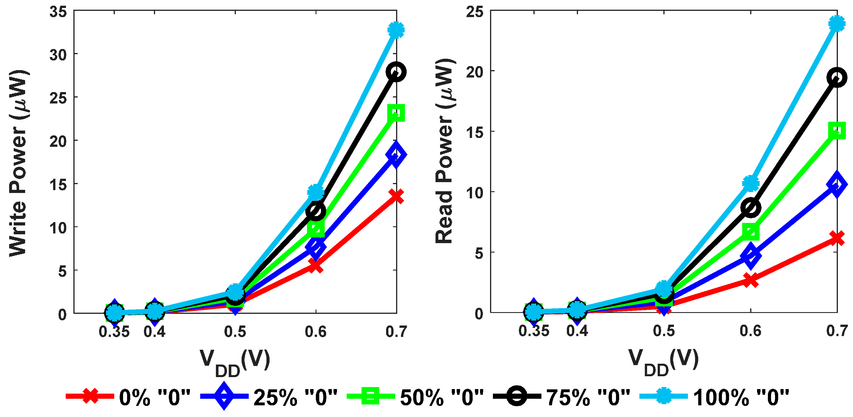
2.3. Power Reduction Features
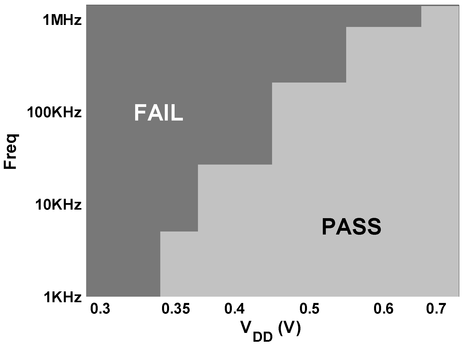
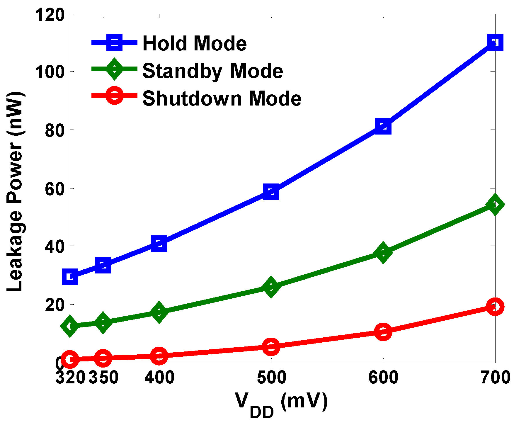
To reduce the power consumption of the array, three low power modes—Hold, Standby and Shutdown—were added. In the Hold mode, the SoC is not accessing the memory, thus the ENABLE signal is held low, and the clock signal to the memory is gated. When the SoC is in a low power state, the data memory SRAM array can be completely shut down while the instruction memory SRAM array can be placed in a low power data retention (Standby) mode. In the Shutdown Mode, the complete array is power gated, and the data is lost. In the Standby Mode, only the peripherals are power gated while the row and column drivers and the bit-cell array retain their state. The row and column drivers isolate the power gated circuits from the on-circuits when the STDBY signal is enabled. The row driver will keep RWL and WWL held low and VVSS held high, and the column drivers will hold BL/BLB low and RBL high.

3. Chip Results

The proposed array was fabricated in a commercial 130 nm bulk CMOS technology (Figure 6) and tested at room temperature. The chip operates for both read and write broadly in the sub-threshold region between 350 mV and 700 mV (Figure 7), and can retain data down to 320 mV.
Figure 8 shows the standby power consumption of the array in the three supported modes: Hold Mode, Standby Mode, and Shutdown Mode. The power consumption of the array is minimized at the data retention voltage of 320 mV to 29.49 nW, 12.29 nW, and 1.09 nW in the Hold, Standby, and Shutdown modes, respectively. The Standby and Shutdown modes are particularly useful for instruction and data memories, respectively, in battery-less SoCs when energy harvesting resources are scarce.
The read and write energies (Figure 9) are minimized at 400 mV to 5.41 pJ/access and 7.08 pJ/access, respectively, assuming equal percentages of “0” and “1” bits within each word. The read burst mode can provide up to 22% reduction in active read energy at 400 mV when enabled. Measurement results show that the charge pump circuits used to boost RWL, WWL and VVSS driver consumes only 3% of the total read/write power at 400 mV.
As discussed in Section 2.1.1, the percentage of “0” bits within a word impacts the read power consumption due to the discharging of RBL during a read “0”. Since a read-before-write approach is used to address half-select failures, the percentage of “0” bits will also impact the write power. Figure 10 shows the read and write power for different percentages of “0” bits within a word. Reducing the percentage of “0” bits from 50% to 25% will result in a maximum of ~30% and ~21% reduction in the read and write power at 0.6 V.
Table 4 shows a comparison between the measured results of our chip and previously presented designs. The active energy per bit and leakage power per bit shown in the table take into account the energy/power consumed in the peripheral logic. The active energy per bit is calculated as the average of the read and write energies per accessed bit. Our design shows the lowest standby power consumed per bit of memory at 1.5 pW/bit for an 8T SRAM cell, making it ideally suited for battery-less SoCs with multiple operating modes.

4. Conclusions

This paper presented a 1 KB SRAM chip fabricated in 130 nm CMOS that operates between 350 mV and 700 mV for ULP sub-threshold operation. High-VT devices are used within the 8T bit-cell in the array. Read and write assist techniques are introduced to guarantee correct operation. A read-before-write approach is implemented to address half-select instability. The read and write energy is minimized at 400 mV. A read burst mode is implemented to reduce read energy when consecutive addresses are accessed and saves 22% of the active read energy. Increasing the percentage of “1” bits within a word allows significant reduction in both the read and write power. Aggressive power gating reduces the power consumption down to 12.29 nW with retention and 1.09 nW when data is not needed (at the data retention voltage of 320 mV). Compared to the state-of-the-art ULP SRAMs, the proposed design gives the lowest full array leakage power per bit at 1.5 pW/bit for an 8T bit-cell array.

Acknowledgments

The authors thank Nicholas Brennan and Ningxi Lui for their support and NVIDIA (DARPA PERFECT) and the NSF NERC ASSIST Center (EEC-1160483) for funding. This research was, in part, funded by the U.S. Government. The views and conclusions contained in this document are those of the authors and should not be interpreted as representing the official policies, either expressed or implied, of the U.S. Government.

Author Contributions

In this work, Farah and Harsh designed the high-VT SRAM cell and ran comprehensive simulations of the read and write operation with their corresponding assist techniques. Farah also worked on the burst control circuitry, chip layout and testing of the high-VT array. She was responsible for the literature review and writing of this paper. In addition to his help in the design and simulation of the cell, Harsh also simulated and compared the charge pump and level converter circuitry, generated the pad ring of the chip and ran top level simulations of the complete array. James designed the read before write circuitry while Arijit designed the initial version of the read burst mode circuitry. Calhoun has guided the design of the array, giving crucial feedback on the different trends seen in the simulation results. He also guided the writing of the paper and its technical proofing.

Conflicts of Interest

The authors declare no conflict of interest.

References

  1. Klinefelter, A.; Roberts, N.E.; Shakhsheer, Y.; Gonzalez, P.; Shrivastava, A.; Roy, A.; Craig, K.; Faisal, M.; Boley, J.; Seunghyun, O.; et al. 21.3 A 6.45 μW self-powered IoT SoC with integrated energy-harvesting power management and ULP asymmetric radios. In Proceedings of the IEEE International Solid- State Circuits Conference (ISSCC), San Francisco, CA, USA, 22–26 February 2015; pp. 1–3.
  2. Zhang, Y.; Zhang, F.; Shakhsheer, Y.; Silver, J.D.; Klinefelter, A.; Nagaraju, M.; Boley, J.; Pandey, J.; Shrivastava, A.; Carlson, E.J.; et al. A Batteryless 19 μW MICS/ISM-Band Energy Harvesting Body Sensor Node SoC for ExG Applications. IEEE J. Solid State Circuits 2013, 48, 199–213. [Google Scholar] [CrossRef]
  3. Calhoun, B.; Wang, A.; Chandrakasan, A.P. Modeling and Sizing for Minimum Energy Operation in Subthreshold Circuit. J. Solid State Circuits 2005, 40, 1778–1786. [Google Scholar] [CrossRef]
  4. Verma, N.; Chandrakasan, A.P. A 256 kb 65 nm 8T Subthreshold SRAM Employing Sense-Amplifier Redundancy. J. Solid State Circuits 2008, 43, 141–149. [Google Scholar] [CrossRef]
  5. Lutkemeier, S.; Jungeblut, T.; Berge, H.K.O.; Aunet, S.; Porrmann, M.; Ruckert, U. A 65nm 32 b Subthreshold Processor with 9T Multi-Vt SRAM and Adaptive Supply Voltage Control. J. Solid State Circuits 2013, 48, 8–19. [Google Scholar] [CrossRef]
  6. Meinerzhagen, P.; Andersson, O.; Mohammadi, B.; Sherazi, Y.; Burg, A.; Rodrigues, J.N. A 500 fW/bit 14 fJ/bit-access 4 kb standard-cell based sub-VT memory in 65 nm CMOS. In Proceedings of the ESSCIRC, 2012, Bordeaux, France, 17–21 September 2012; pp. 321–324.
  7. Kulkarni, J.; Khellah, M.; Tschanz, J.; Geuskens, B.; Jain, R.; Kim, S.; De, V. Dual-VCC 8T-bitcell SRAM Array in 22 nm tri-gate CMOS for energy-efficient operation across wide dynamic voltage range. In Proceedings of the IEEE Symposium on VLSI Circuits (VLSIC), Kyoto, Japan, 11–13 June 2013.
  8. Raychowdhury, A.; Geuskens, B.; Kulkarni, J.; Tschanz, J.; Bowman, K.; Karnik, T.; Lu, S.-L.; De, V.; Khellah, M.M. PVT-and-Aging Adaptive Wordline Boosting for 8T SRAM Power Reduction. In Proceedings of the IEEE International Solid-State Circuits Conference, San Francisco, CA, USA, 7–11 February 2010; pp. 352–353.
  9. Chang, I.J.; Kim, J.-J.; Park, S.P.; Roy, K. A 32 kb 10T sub-threshold SRAM array with bit-interleaving and differential read scheme in 90 nm CMOS. J. Solid State Circuits 2009, 44, 650–658. [Google Scholar] [CrossRef]
  10. Kim, T.H.; Liu, J.; Keane, J.; Kim, C.H. A High-Density Subthreshold SRAM with Data-Independent Bitline Leakage and Virtual Ground Replica Scheme. In Proceedings of the IEEE International Solid-State Circuits Conference, San Francisco, CA, USA, 11–15 February 2007; pp. 330–606.
  11. Ghaed, M.H.; Chen, G.; Haque, R.-U.; Wieckowski, M.; Kim, Y.; Kim, G.; Lee, Y.; Lee, I.; Fick, D.; Kim, D.; et al. Circuits for a Cubic-Millimeter Energy-Autonomous Wireless Intraocular Pressure Monitor. IEEE Trans. Circuits Syst. I Regul. Pap. 2013, 60, 3152–3162. [Google Scholar] [CrossRef]
  12. Liu, X.; Zhou, J.; Yang, Y.K.; Wang, B.; Lan, J.J.; Wang, C.; Luo, J.W.; Wang, L.G.; Kim, T.T.-H.; Minkyu, J. A 457 nW Near-Threshold Cognitive Multi-Functional ECG Processor for Long-Term Cardiac Monitoring. J. Solid State Circuits 2014, 49, 2422–2434. [Google Scholar] [CrossRef]
  13. Yahya, F.B.; Patel, H.N.; Chandra, V.; Calhoun, B.H. Combined SRAM read/write assist techniques for near/sub-threshold voltage operation. In Proceedings of the Asia Symposium on Quality Electronic Design (ASQED), Kula Lumpur, Malaysia, 4–5 August 2015; pp. 1–6.
  14. Sinangil, M.E.; Chandrakasan, A.P. Application-Specific SRAM Design Using Output Prediction to Reduce Bit-Line Switching Activity and Statistically Gated Sense Amplifiers for Up to 1.9x Lower Energy/Access. J. Solid State Circuits 2014, 49, 107–117. [Google Scholar] [CrossRef]
  15. Stan, M.R.; Burleson, W.P. Bus-invert coding for low-power I/O. IEEE Trans. Very Large Scale Int. (VLSI) Syst. 1995, 3, 49–58. [Google Scholar] [CrossRef]
  16. Chandra, V.; Pietrzyk, C.; Aitken, R. On the efficacy of write-assist techniques in low voltage nanoscale SRAMs. In Proceedings of the Design, Automation & Test in Europe Conference & Exhibition (DATE), Dresden, Germany, 8–12 March 2010; pp. 345–350.
  17. Guo, Z.; Carlson, A.; Pang, L.-K.; Duong, K.; Liu, T.-J.K.; Nikolic, B. Large-scale read/write margin measurement in 45nm CMOS SRAM arrays. In Proceedings of the IEEE Symposium on VLSI Circuits, Honolulu, HI, USA, 18–20 June 2008; pp. 42–43.
  18. Wang, Y.; Hong, J.A.; Bhattacharya, U.; Chen, Z.P.; Coan, T.; Hamzaoglu, F.; Hafez, W.M.; Jan, C.-H.; Kolar, P.; Kulkarni, S.H.; et al. A 1.1 GHz 12 μA/Mb-leakage SRAM design in 65 nm ultra-low-power CMOS technology with integrated leakage reduction for mobile applications. J. Solid State Circuits 2008, 43, 172–179. [Google Scholar] [CrossRef]
  19. Sinangil, M.E.; Verma, N.; Chandrakasan, A.P. A reconfigurable 65nm SRAM achieving voltage scalability from 0.25 to 1.2 V and performance scalability from 20 kHz to 200 MHz. In Proceedings of the ESSCIRC 2008 34th European Solid-State Circuits Conference, Edinburgh, UK, 15–19 September 2008.
  20. Kim, D.; Chen, G.; Fojtik, M.; Seok, M.; Blaauw, D.; Sylvester, D. A 1.85fW/bit ultra low leakage 10T SRAM with speed compensation scheme. In Proceedings of the IEEE International Symposium on Circuits and Systems (ISCAS), Rio de Janeiro, Brazil, 15–18 May 2011; pp. 69–72.
  21. Chang, M.F.; Chen, M.P.; Chen, L.F.; Yang, S.M.; Kuo, Y.J.; Wu, J.J.; Su, H.Y.; Chu, Y.H.; Wu, W.C.; Yang, T.Y.; et al. A Sub-0.3 V Area-Efficient L-Shaped 7T SRAM With Read Bitline Swing Expansion Schemes Based on Boosted Read-Bitline, Asymmetric-VTH Read-Port, and Offset Cell VDD Biasing Techniques. J. Solid State Circuits 2013, 48, 2558–2569. [Google Scholar] [CrossRef]
  22. Wu, J.J.; Chen, Y.H.; Chang, M.F.; Chou, P.W.; Chen, C.Y.; Liao, H.J.; Chen, M.B.; Chu, Y.H.; Wu, W.C.; Yamauchi, H. A Large σVTH/VDD Tolerant Zigzag 8T SRAM with Area-Efficient Decoupled Differential Sensing and Fast Write-Back Scheme. J. Solid State Circuits 2011, 46, 815–827. [Google Scholar] [CrossRef]
Figure 1. The 8T bit-cell [4].
Jlpea 06 00008 g001
Figure 2. Array block diagram (The array also includes input latches for all input signals (excluding the standby (STDBY), clock (CLK) and Reset signals). It also has a power gating control block that is not included in the figure.)—blocks in gray are power gated during Standby mode.
Jlpea 06 00008 g002
Figure 3. The 3σ write margin vs. VDD for WL Boosting (BWL) and VSS Raising (RVSS).
Jlpea 06 00008 g003
Figure 4. Data Management Unit (DMU) block diagram.
Jlpea 06 00008 g004
Figure 5. Timing diagram for the read and write operations.
Jlpea 06 00008 g005
Figure 6. Die photo of the proposed SRAM array.
Jlpea 06 00008 g006
Figure 7. Measured shmoo plot of the ultra-low power (ULP) SRAM.
Jlpea 06 00008 g007
Figure 8. Measured power consumption during Hold, Standby and Shutdown modes.
Jlpea 06 00008 g008
Figure 9. Measured write and read energy with read burst mode enabled and disabled.
Jlpea 06 00008 g009
Figure 10. Change in read and write power as a function of the number of “0” bits within a word.
Jlpea 06 00008 g010
Table 1. Main Array Features.
Tech.Commercial 130 nm Complementary Metal Oxide Semiconductor (CMOS)
Cell8T static random access memory (SRAM) cell
Size1 Kbyte (64 × 128), 16-bit/word
Voltage350–700 mV
Leakage Power12.29 nW @ 320 mV (standby)
1.09 nW @ 320 mV (shutdown)
E/access6.24 pJ/access @ 400 mV
Special features
  • High-threshold (high-VT) devices
  • Full-swing read
  • Read burst mode
  • Read wordline (RWL) boosting to improve read stability
  • Read-before-write for half-select instability
  • Write wordline (WWL) boosting to improve write stability
  • Aggressive power gating for low power standby and shutdown modes
Table 2. Comparison between high-threshold (high-VT) read port with RWL boosting and nominal-VT read port for read assist (based on chip measurements).
Nominal-VT Read PortHigh-VT Read Port with RWL Boosting
Read frequency114.7 KHz @ 400 mV26.6 KHz @ 400 mV
Leakage Power per bit3.4 pW @ 320 mV1.5 pW @ 320 mV
Read Power per accessed bit35.4 nW @ 400 mV9 nW @ 400 mV
Area overhead (normalized)1x1.05x
Table 3. Read and Write power (in nW/KB) of the array containing different percentages of “0” and “1” bits in each word (based on chip measurements).
(nW)0% “0” bits25% “0” bits50% “0” bits75% “0” bits100% “0” bits
Read Power @ 350 mV41.8346.0750.3154.5658.80
Read Power @ 400 mV83.07113.48143.89174.3204.71
Write Power @ 350 mV44.7449.9955.2460.4965.74
Write Power @ 400 mV123.89156.09188.29220.49252.69
Table 4. Comparison between this work and previously published chips. * total energy reported in fJ since word size was not provided.
Tech.VDDCell TypeTransistor TypeArray(Kb)/Word SizeFreq. (MHz)Energy (fJ/bit)Leakage Power (pW/bit)
This work1300.328THigh VT8/16--1.5
0.40.0273901.7
[4]650.358TN/A256/1280.038708.4
[5]650.39TMixed VT2/320.2218.217.8
0.4221.825.4
[6]650.514THigh VT4/320.11140.5 @ 0.22 V
[18]650.56TLow leakage1024/-250N/A5.7
[19]650.48TLow power64/128~0.06786.1 @ 0.25 V
[20]1800.3510TMixed VT24/320.053N/A0.0019
[21]650.267TN/A32/-1.85600 *-
[22]900.23Z8TN/A64/-0.580,000 *305

