Article

Extensionless UTBB FDSOI Devices in Enhanced Dynamic Threshold Mode under Low Power Point of View †

1
LSI/PSI—Integrated Systems Laboratory/Department of Electronic Systems Engineering, University of Sao Paulo, Av. Prof. Luciano Gualberto, trav.3, n.158, Sao Paulo 05508-010, Brazil
2
IMEC—Interuniversity Microelectronic Centre, Kapeldreef 75, B-3001 Leuven, Belgium
3
Electrical Engineering Department, KU Leuven, Kasteelpark Arenberg 10, B-3001 Leuven, Belgium
*
Author to whom correspondence should be addressed.
The original of this paper had been presented in IEEE S3S Conference 2014.
J. Low Power Electron. Appl. 2015, 5(2), 69-80; https://doi.org/10.3390/jlpea5020069
Submission received: 19 February 2015 / Revised: 16 April 2015 / Accepted: 21 April 2015 / Published: 29 April 2015
(This article belongs to the Special Issue Selected Papers from IEEE S3S Conference 2014)

Abstract

:
This work presents an analysis about the influence of the gate and source/drain underlap length (LUL) on UTBB FDSOI (UltraThin-Body-and-Buried-oxide Fully-Depleted-Silicon-On-Insulator) devices operating in conventional (VB = 0 V), dynamic threshold (DT, VB = VG), and the enhanced DT (eDT, VB = kVG) configurations, focusing on low power applications. It is shown that the underlap devices present a lower off-state current (IOFF at VG = 0 V), lower subthreshold swing (S), lower gate-induced drain leakage (GIDL), higher transconductance over drain current (gm/ID) ratio and higher intrinsic voltage gain (|AV|) due to their longer effective channel length in weak inversion and lower lateral electric field, while the eDT mode presents higher on-state current (ION) with the same IOFF, lower S, higher maximum transconductance (gmmax), lower threshold voltage (VT), higher gm/ID ratio and higher |AV| due to the dynamically reduced threshold voltage and stronger transversal electric field.

1. Introduction

Thanks mainly to its better back gate coupling, ultrathin-body-and-buried-oxide fully-depleted-silicon-on-insulator (UTBB FDSOI) devices present better performance for sub 28 nm technology nodes such as lower short channel effects (SCE) and better threshold voltage control, while keeping the planar structure [1,2,3,4,5]. Also, they can be used at high frequencies with a lower back gate leakage, lower voltage operation and better power efficiency [4,6]. Moreover, by using a Ground Plane (GP) implantation, the threshold voltage can be adjusted without increasing the channel doping, which avoids mobility degradation and random-dopant fluctuations [7]. This region diminishes the depletion thickness underneath the buried oxide layer, reducing the source and drain electric field that reaches the channel through the buried oxide [7,8,9].
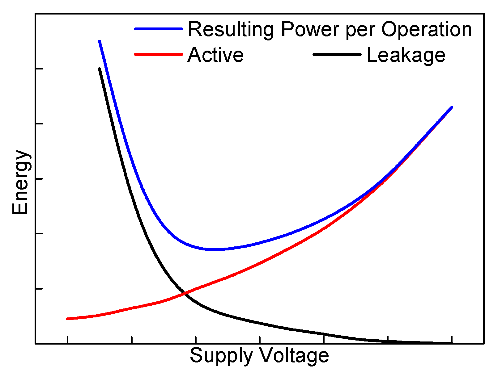
In circuits, a reduced minimum energy consumption has been demonstrated, which occurs at a lower supply voltage [6], when compared to bulk CMOS devices. This minimum energy consumption is a tradeoff between the leakage and the active current, as indicated in Equation (1) and Figure 1 [10].
P = C V D D 2 f A c t i v e + I l e a k V D D L e a k a g e
Figure 1. Energy consumption as a function of the supply voltage [10].
Jlpea 05 00069 g001
With its lower lateral electric field and longer effective channel length, extensionless devices, also known as underlap devices, have demonstrated a better SCE, providing a more scalable structure, better analog performance, and advantages in memory applications [11,12,13,14,15]. Moreover, they have shown a better subthreshold behavior, which in the weak inversion regime is favorable for low power low voltage applications [16].
Originally, the dynamic threshold (DT) concept was explored in partially depleted SOI (PDSOI) devices as a way to avoid the floating body problems. The gate and the body are short-circuited; consequently, the body is never floating [17]. However, the bulk-drain junction can be forward biased if the gate voltage is higher than 0.7 V, which is a disadvantage for these devices. Recently, with the advent of UTBB devices, a new generation of dynamic threshold voltage configuration (DT2) has been studied [3,18]. In this case, the front gate is connected to the back-gate and the same concept is achieved: during the VG sweep, the threshold voltage (VT) is dynamically reduced, as it is a function of the VBody (in PDSOI) or VB (in UTBB), which is equal to VG, improving the device performance [17].
Some optimizations have been reported about this approach, regarding the ground plane and the channel length influence in these operation modes [19] or the impact of the silicon film thickness [20]. The effect of the buried oxide thickness on the analog figures of merits has been studied [20,21,22,23], as well as the circuit for generating the back gate of the eDT mode for a sleep transistor, taking into account the back gate capacitance influence on the circuit performance. Finally, the application of the dynamic threshold technique in UTBB devices as a power switch has also been discussed [24].
Therefore, the goal of this work is to compare the impact of the underlap length (LUL), including the self-aligned devices (LUL = 0 nm), on UTBB SOI MOSFETs when submitted to a conventional and a dynamic threshold voltage (DT2) configuration, focusing on low power low voltage applications. In order to enhance the back gate influence on VT, a back gate bias with a multiple value of the front gate voltage (VB = k × VG) is also used [3,18], with k > 1, which is called the eDT mode in this paper.

2. Device Description

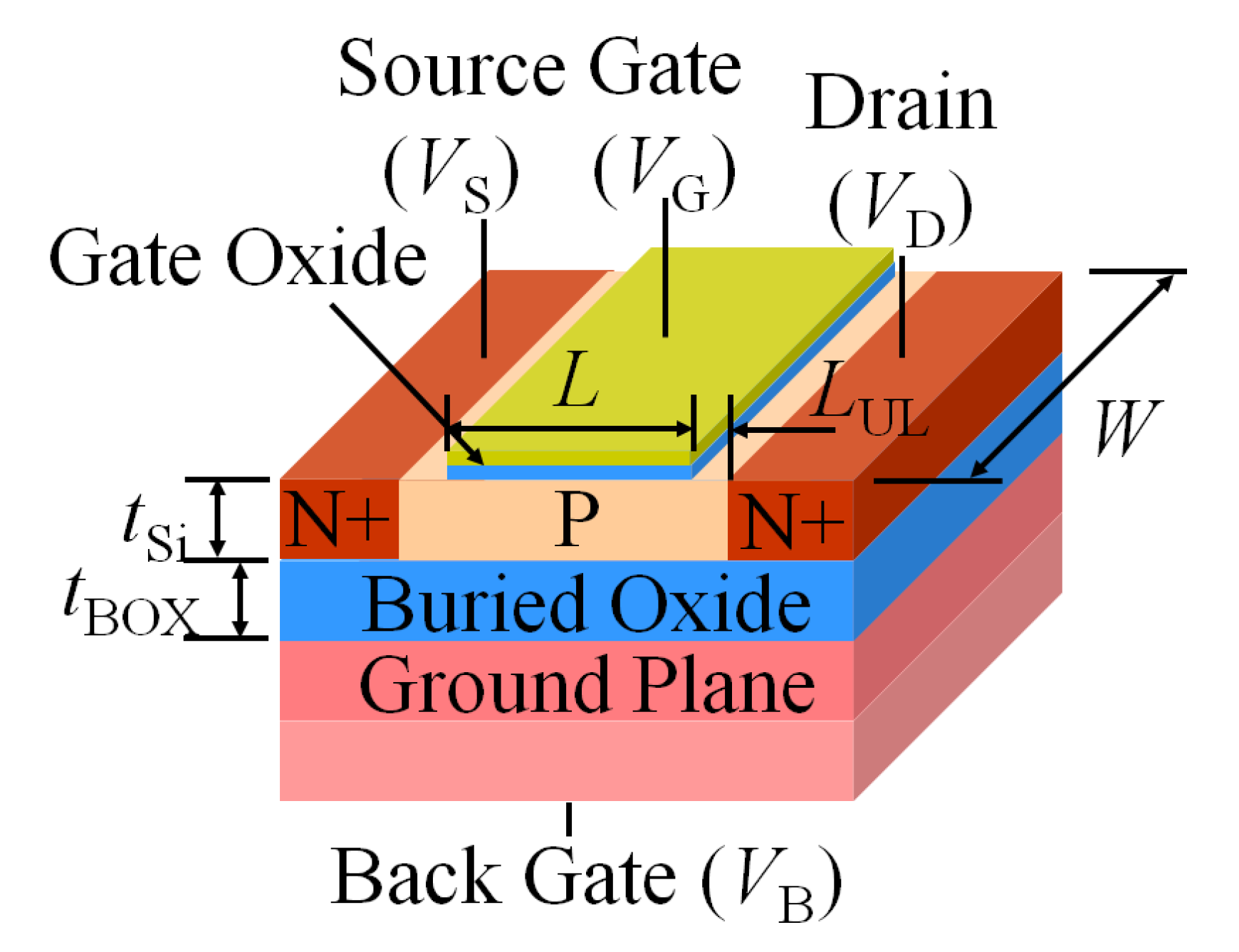
Figure 2 shows the structure of an extensionless UTBB FDSOI device. The devices were built on 300 mm diameter SOI wafers with a 20 nm silicon film (tSi) and 10 nm buried oxide (tBOX). A B-implantation was performed for GP doping. The gate stack is composed by 5 nm SiO2 and a 5 nm plasma enhanced atomic layer deposition (PEALD) TiN layer capped with 100 nm a-Si. A low energy As-implantation was performed on the standard nMOSFETs (self-aligned with lightly-doped drain—LDD) for the extensions while extensions were left free for the extensionless ones. This was followed by a formation of a first nitride spacer of 15 nm or 20 nm width and of the implanted Si-epitaxial raised Source-Drain (SEG) As-HDD (highly-doped drain) [25]. After the HDD a second nitride spacer is formed followed by silicidation and a standard back-end of line process. The effective channel length (Leff) and width (W) were fixed to 70 nm and 920 nm, respectively. The underlap lengths (LUL) are 0 nm (for the self-aligned devices with LDD), or the first spacer width (15 nm or 20 nm).
Figure 2. Extensionless UTBB FDSOI (ultrathin-body-and-buried-oxide fully-depleted-silicon-on-insulator) structure considered in this work.
Jlpea 05 00069 g002
It is important to mention that devices with an underlap of 10 nm have been analyzed in [26]. They presented a worse behavior than the self-aligned devices, due to the shorter effective channel length. These devices have a larger difference between the doping concentration of the channel and the source and drain regions, which increase the lateral diffusion [26]. Therefore, this case will not further be discussed here.

3. Results and Discussion

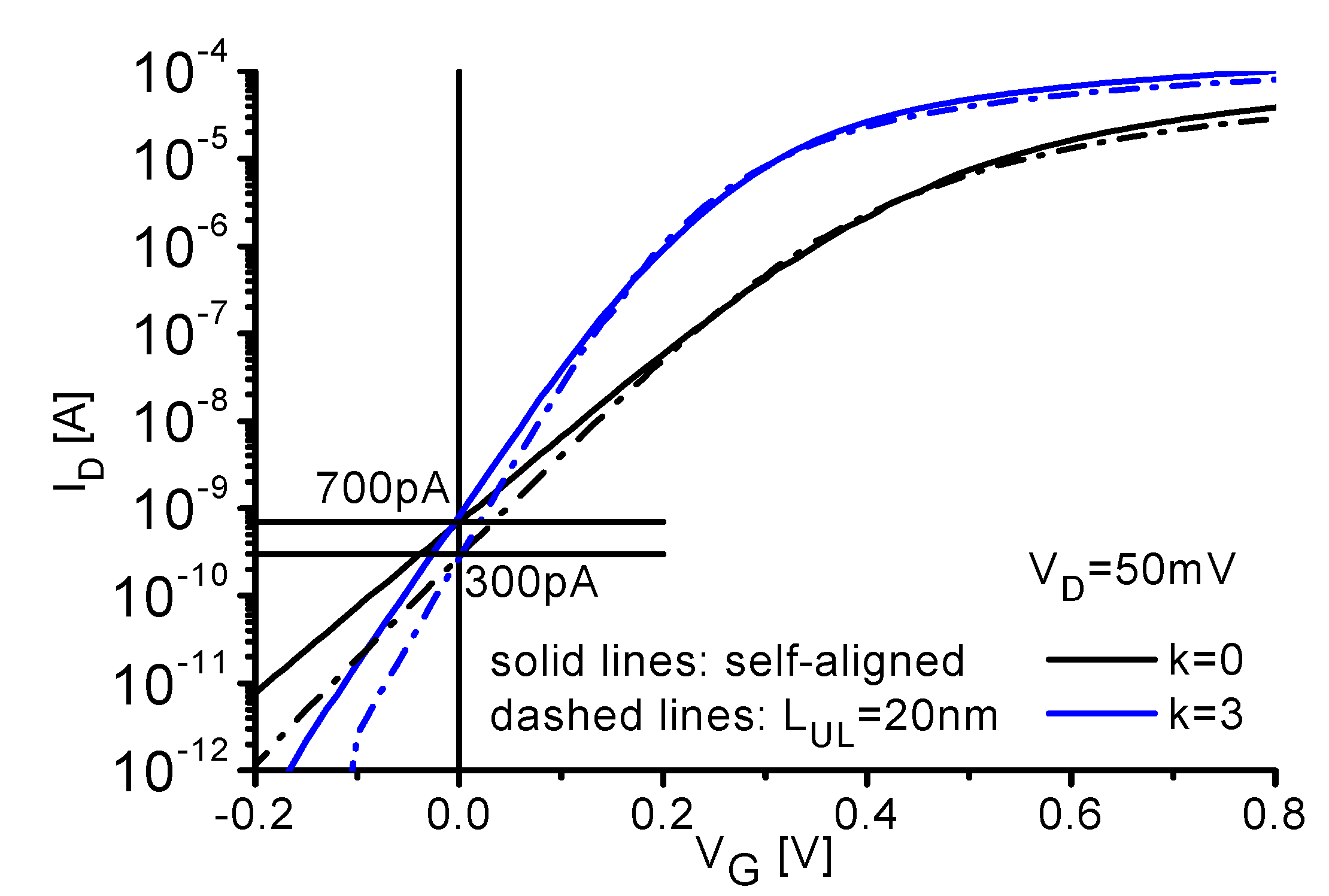
The ID-VG (drain current as a function of front gate voltage) characteristics are presented in Figure 3 for the self-aligned case and for an underlap of 20 nm in the conventional and the eDT (k = 3) modes.
Figure 3. Drain current versus front gate voltage for self-aligned and an underlap length of 20nm in conventional and eDT (k = 3) operation. Leff = 70 nm, Weff = 920 nm, tSi = 14 nm, tBOX = 18 nm.
Jlpea 05 00069 g003
Table 1. ION/IOFF ratio for self-aligned and an underlap length of 20 nm and for conventional and eDT (k = 3) configurations. IOFF @ VG = 0V and ION @ VGT = 200 mV. Leff = 70 nm, Weff = 920 nm, tSi = 14 nm, tBOX = 18 nm.
Self-Aligned, k = 0Self-Aligned, k = 3LUL = 20 nm, k = 0LUL = 20 nm, k = 3
3.08 × 1046.54 × 1046.48 × 10410.52 × 104
One can observe in Figure 3 a lower IOFF (at VG = 0V), i.e., a lower off-state current, for underlap devices in the conventional mode. A lower off-current is aimed in order to reduce the power dissipation during off-state. This behavior can be due to the longer Leff, and better SCE. This remains in the eDT mode, since the back gate bias applied in both cases is the same. As the devices reach weak inversion, the Leff approaches LG and the ID of the underlap device becomes closer to the self-aligned counterpart [15]. In strong inversion, the ID decreases around 10% due to the higher total resistance of the underlap devices, but IOFF reduces around 57% [14]. Also, when the back gate bias is increased (in DT and eDT conditions) the threshold voltage reduces dynamically and a higher ION can be achieved. This results in a higher ION/IOFF ratio for underlap devices in eDT mode (Table 1).
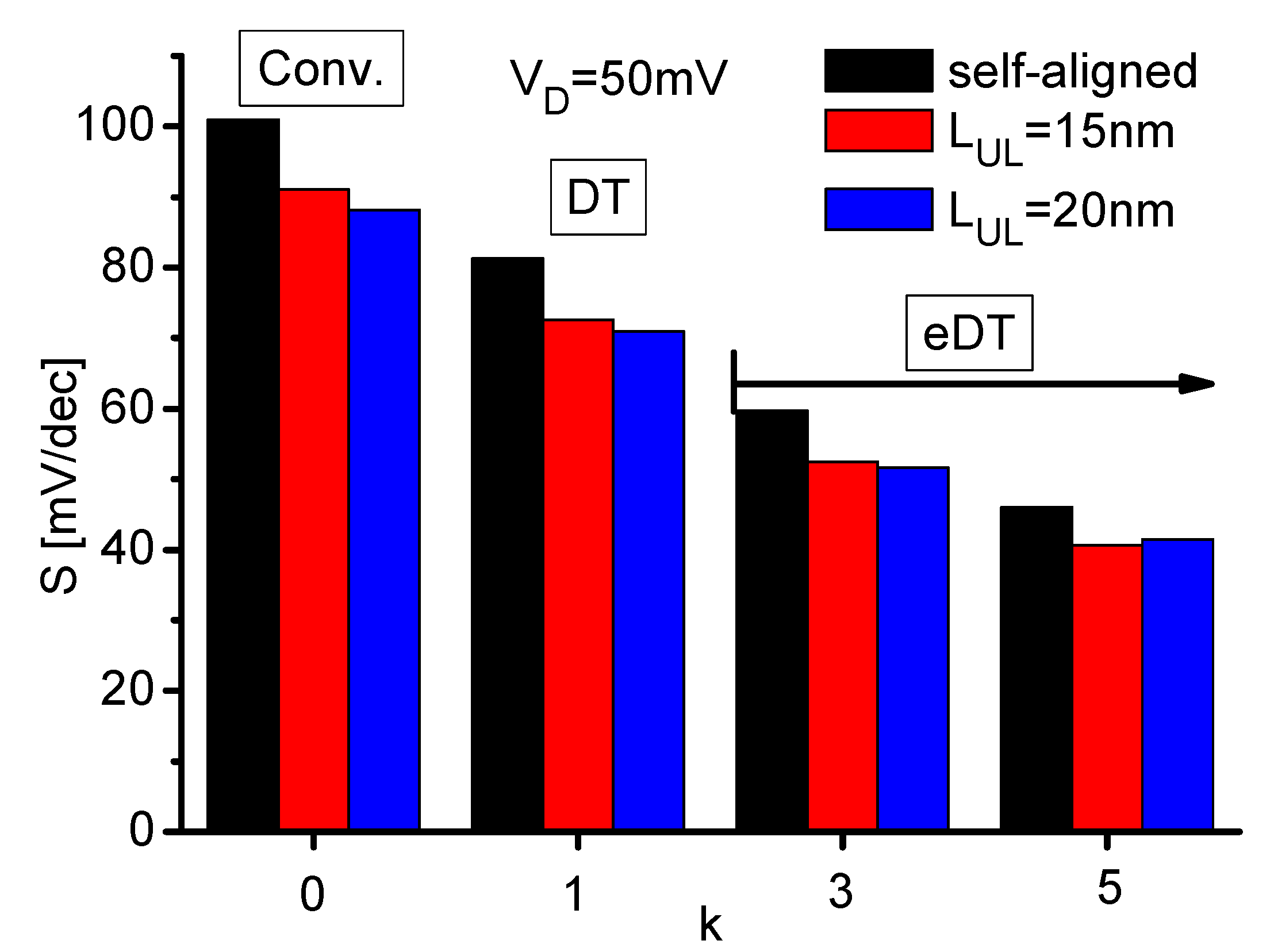
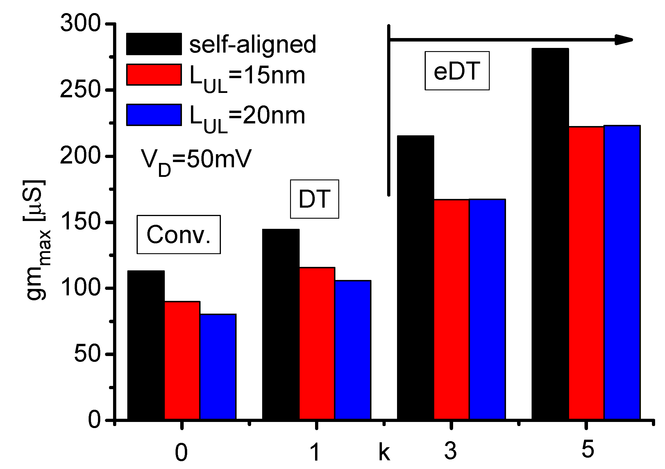
The subthreshold swing (S) and the maximum transconductance were extracted and are presented as a function of the k-values for three underlap lengths in Figure 4 and Figure 5.
Figure 4. Subthreshold swing for various k-values and underlap lengths (based on reference [27]). Leff = 70 nm, Weff = 920 nm, tSi = 14 nm, tBOX = 18 nm.
Jlpea 05 00069 g004
Figure 5. Maximum transconductance for various k-values and underlap lengths (based on reference [27]). Leff = 70 nm, Weff = 920 nm, tSi = 14 nm, tBOX = 18 nm.
Jlpea 05 00069 g005
The higher ID variation with VG shown in Figure 1 for underlap devices, and now also with VB for higher k values, leads to a lower subthreshold swing, which is important for low power devices by enabling reduced supply voltages [28]. Moreover, although the underlap devices present a lower maximum transconductance due to the higher total resistance, the eDT mode can overcome this drawback.
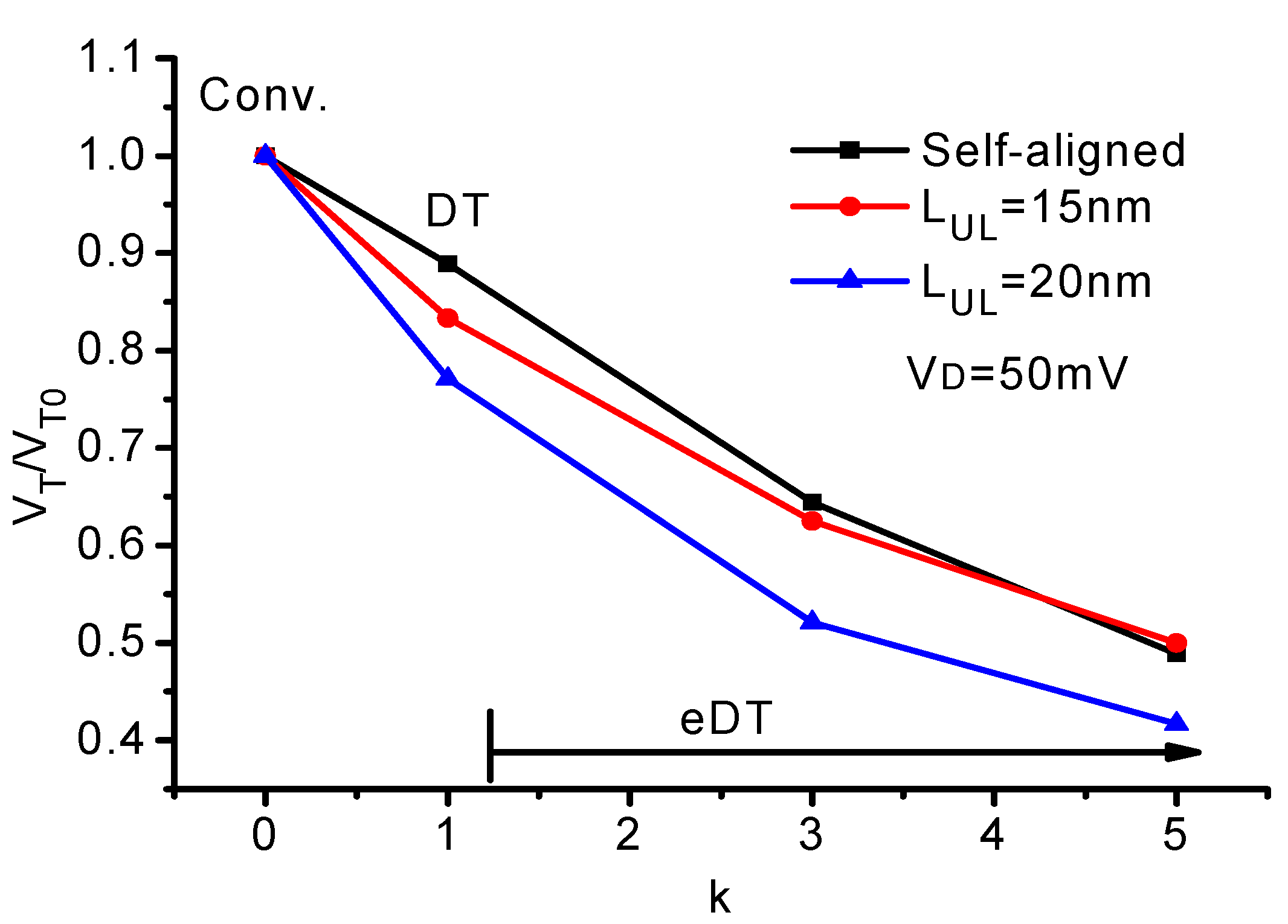
Another important aim for low power applications is the reduction of the threshold voltage without raising the off-current, since it means a lower supply voltage added to a constant, or lower, leakage current Equation (1) [10]. Table 2 and Figure 6 show, respectively, the absolute and normalized threshold voltage for the three devices studied and for various k-values.
As expected, the threshold voltage decreases for higher k values due to the stronger DT effect (Table 2). This effect can also be strengthened by the lower lateral electric field for a higher underlap, which is seen by a lower normalized threshold voltage for DT and eDT in Figure 6.
Table 2. Threshold voltage for various k-values and underlap lengths (based on reference [27]). Leff = 70 nm, Weff = 920 nm, tSi = 14 nm, tBOX = 18 nm.
kThreshold Voltage [V]
Self-AlignedLUL = 15 nmLUL = 20 nm
00.450.480.48
10.400.400.37
30.290.300.25
50.220.240.20
Figure 6. Normalized threshold voltage for various k-values and underlap lengths (based on reference [27]). Leff = 70 nm, Weff = 920 nm, tSi = 14 nm, tBOX = 18 nm.
Jlpea 05 00069 g006
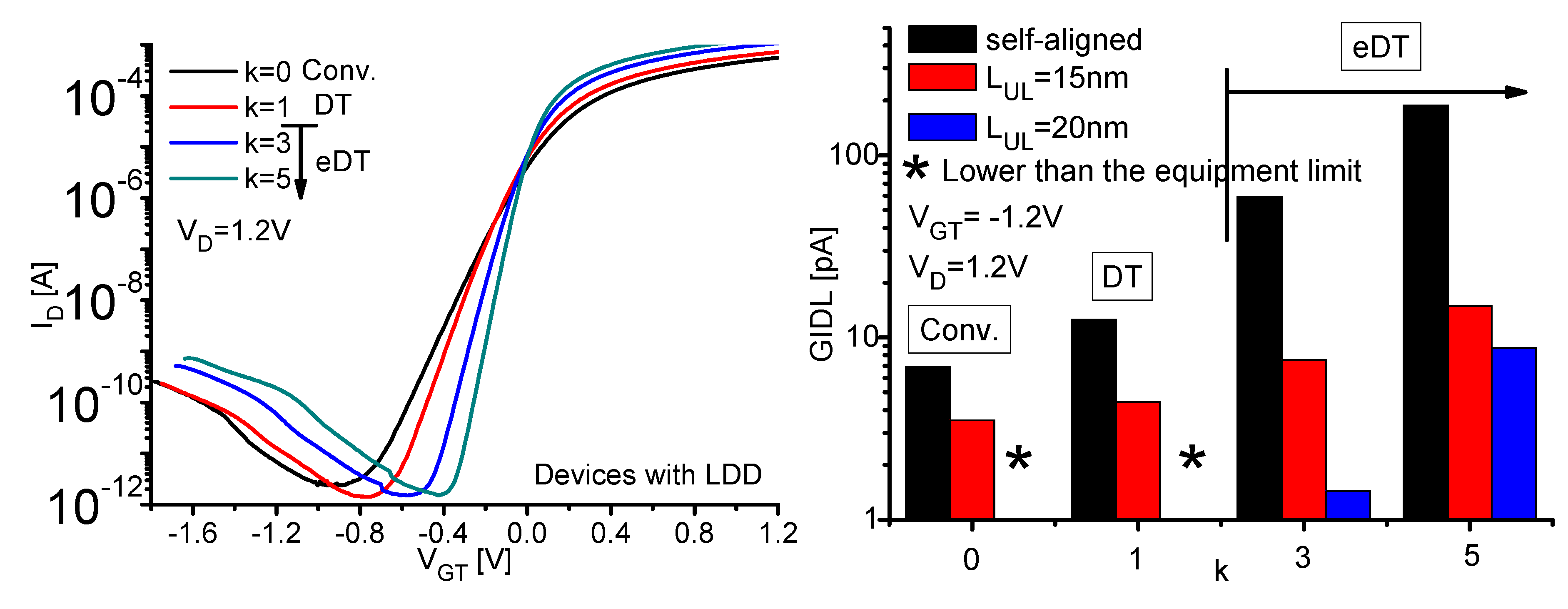
Concerning the leakage current, there is also the gate-induced-drain-leakage (GIDL), which can be seen in Figure 7 for various k values as a ID-VGT (drain current versus gate overdrive, where VGT = VGVT) characteristics (left) and for the three devices studied (right).
Figure 7. Drain current versus overdrive voltage for VD = 1.2 V for various k-values (left) and gate-induced-drain-leakage for different k-factors and underlap lengths (right) (based on reference [27]). Leff = 70 nm, Weff = 920 nm, tSi = 14 nm, tBOX = 18 nm.
Jlpea 05 00069 g007
Concerning the leakage current, as it has already been shown before, IOFF (at VG = 0V) is lower in underlap devices and is the same in DT and eDT modes. Besides, it is possible to see, in Figure 7, a higher GIDL in DT and eDT modes, most probably due to a lower potential induced by the lower VB. For higher k-values, the difference between the front and back gate potential increases, enhancing the transversal electric field. This can generate more tunneling charges near the drain, worsening this leakage. However, underlap devices reduce drastically this leakage by a lower lateral electric field [29]. One can notice from the right side of Figure 7, for example, that the 20 nm-underlap for k = 5 presents almost the same value than the self-aligned counterpart in the conventional mode.
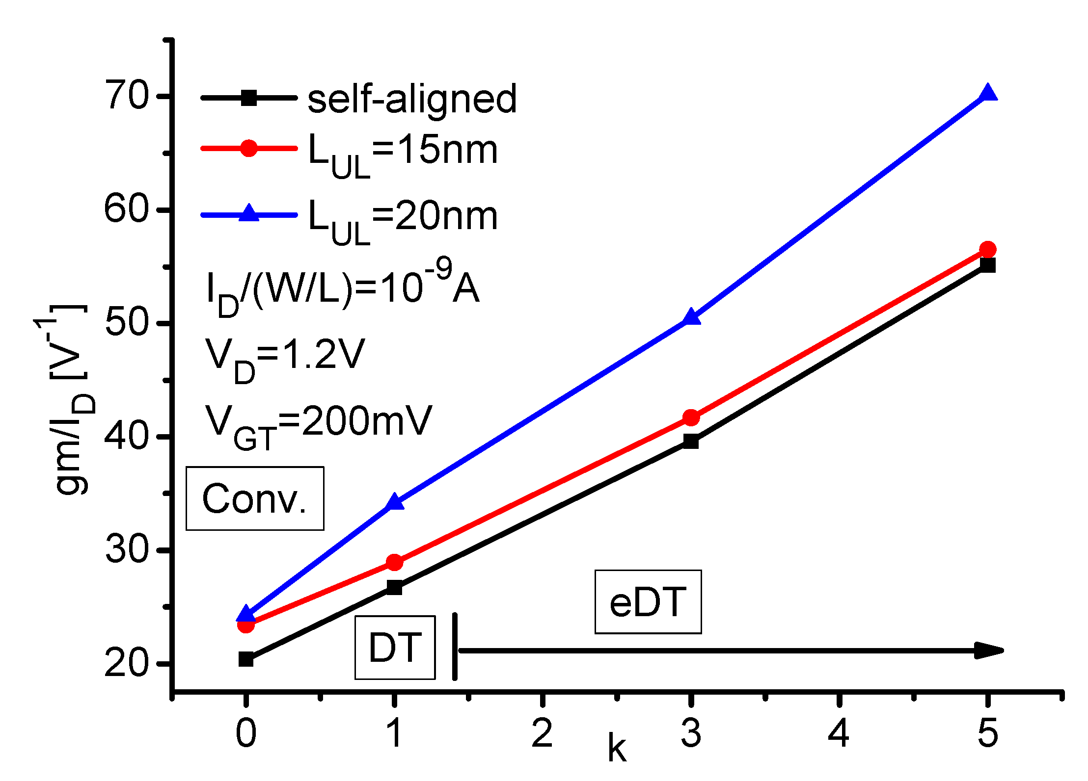
Figure 8 shows the transistor efficiency, i.e., the transconductance over drain current ratio (gm/ID) for various k values and for the three underlap lengths in weak inversion, at a normalized ID/(W/L) of 1 nA.
Figure 8. Transconductance over drain current ratio in weak inversion for various k-values and underlap lengths at a normalized drain current of 1nA (based on reference [27]). Leff = 70 nm, Weff = 920 nm, tSi = 14 nm, tBOX = 18 nm.
Jlpea 05 00069 g008
A higher efficiency is observed for longer underlap and higher k values, due to the lower subthreshold swing (Figure 4). In other words, one can achieve a higher amplification with the same supply energy in underlap devices in DT and eDT modes.
The intrinsic voltage gain of the studied devices is given for various k values in Figure 9.
Figure 9. Intrinsic voltage gain for various k-values and underlap lengths (based on reference [27]). Leff = 70 nm, Weff = 920 nm, tSi = 14 nm, tBOX = 18 nm.
Jlpea 05 00069 g009
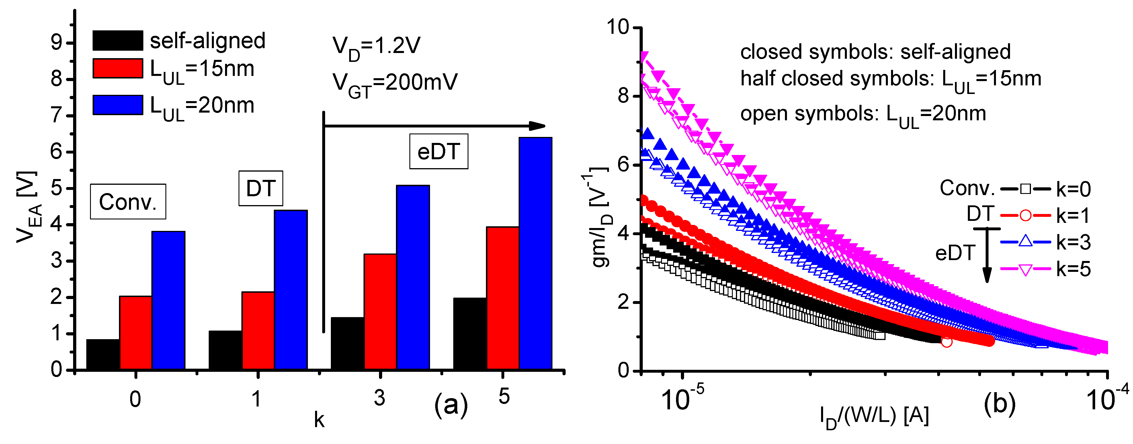
One observes an increased intrinsic voltage gain (|AV|) for longer underlap and higher k-values. Since |AV| = VEA × gm/ID, Figure 10 shows the Early voltage (VEA) and the gm/ID in strong inversion for various k values and underlap lengths.
Figure 10. Early voltage (a) and transconductance over drain current ratio in strong inversion (b) for various k-values and underlap lengths (based on reference [27]). Leff = 70 nm, Weff = 920 nm, tSi = 14 nm, tBOX = 18 nm.
Jlpea 05 00069 g010
Although there is a slight reduction of the gm/ID in strong inversion for longer underlap (Figure 10b) due to the higher total resistance [12,27], it is negligible when compared to the improvement of VEA (Figure 10a), thanks to the lower lateral electric field [12,29]. Therefore, the main reason for the |AV| tendency is the substantial reduction of the lateral electric field and, consequently, a higher Early voltage (Figure 10a). Also, a higher influence of the transversal electric field can improve this parameter in DT and eDT operations.
Regarding the k values, both, the gm/ID and VEA, increase for higher k values in strong inversion (Figure 10a,b).
About the gm/ID in strong inversion, as it is a drawback for longer underlap, one can observe that, for example, the self-aligned transistor in the conventional mode presents almost the same value than the 20 nm-underlap device for k = 1. This means that the eDT mode is overcoming the undesired trend.
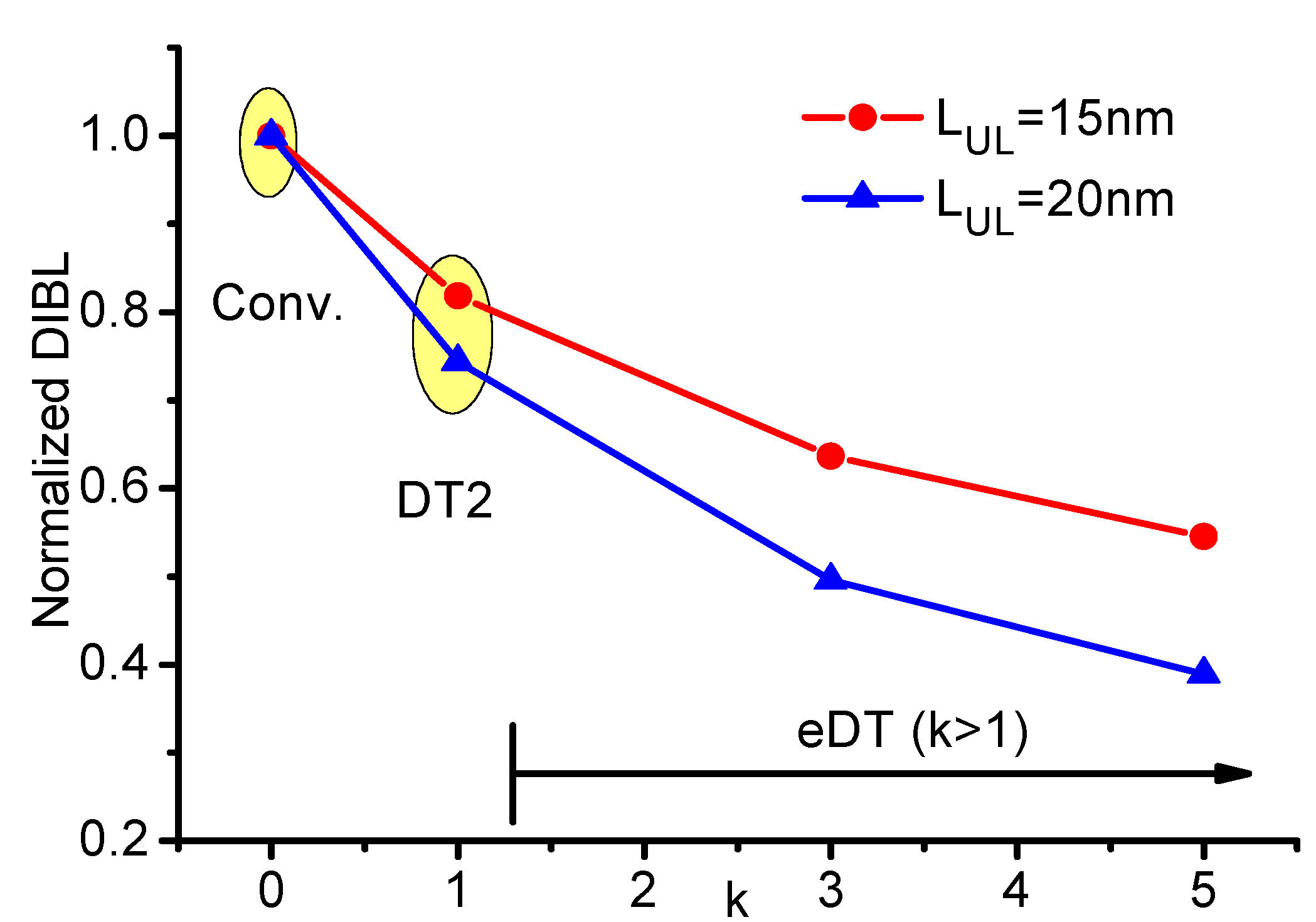
In order to better evaluate the correlation between the lateral and the transversal electric field, Figure 11 shows the DIBL (Drain Induced Barrier Lowering) for devices with 20 nm and 15 nm underlap in the 3 operation modes considered.
In this figure, the DIBL can represent an estimation of the drain electric field existing in the channel. On the other hand, the k-values can be seen as operating on the transversal electric field, since a higher k-value leads to a higher difference between the front and the back interface potential.
One can observe a higher variation for the 20 nm-underlap case than for 15 nm when a higher k value is applied. It means that the longer underlap, which corresponds with a lower lateral electric field, is more susceptible to the dynamic threshold effect. In other words, the higher transversal electric field, resulting from a higher k-factor, strongly acts when the lateral electric field is lower.
Figure 11. Normalized DIBL as a function of k-value for an underlap of 15 nm and 20 nm (based on reference [27]). Leff = 70 nm, Weff = 920 nm, tSi = 14 nm, tBOX = 18 nm.
Jlpea 05 00069 g011

4. Conclusions

The impact of the underlap length, including the self-aligned LDD device, on the main parameters was analyzed for three operation conditions: the conventional (VB = 0 V), the standard dynamic threshold (DT, VB = VG) and the enhanced DT (eDT, VB = kVG), focusing on low power applications.
For low power low voltage applications, the best results were S ≅ 41 mV/dec, VT = 0.2 V, gm/ID ≈ 70 V−1 (in weak inversion) and |AV| ≈ 34 dB for the 20 nm-underlap device, a channel length of 70 nm and in eDT mode.
Although the longer underlap presented a lower ON-current and transconductance due to the higher total resistance, the dynamic threshold reduction compensates these drawbacks. On the other hand, a longer underlap substantially diminishes the GIDL current, which is a negative point of the dynamic threshold and enhanced modes, since it also means a more negative back gate bias. Looking at the OFF-current, the ION/IOFF ratio, the subthreshold swing, the threshold voltage, the gm/ID ratio and the intrinsic voltage gain, both features, longer underlap and eDT, mode improve these parameters.
Moreover, longer underlap devices are more susceptible with the increase of the k-factor, leading to a further performance improvement. This can be explained by the lower lateral electric field and higher influence of the transversal one, which strengthen the dynamic threshold effect.
Thus, the eDT mode or underlap devices alone present important shortcomings for low power low voltage applications, such as higher GIDL for eDT mode and lower ION and gm/ID ratio for underlap devices. However, combined, they compensate the drawback of the other feature. The 20 nm-underlap device in eDT mode with k = 5 presented about the same GIDL current than the self-aligned transistor in the conventional mode. And even for k = 3, the eDT mode improves the lower ION and gm/ID ratio shown by the longer underlap.
Therefore, the 20 nm-underlap device in eDT mode with k = 5 presented the best performance for low power low voltage applications, by enabling a low supply voltage together with a low leakage current.

Acknowledgments

The authors acknowledge FAPESP (Fundação de Amparo à Pesquisa do Estado de Sao Paulo), CAPES (Coordenação de Aperfeiçoamento de Pessoal de Nível Superior), CNPq (Conselho Nacional de Desenvolvimento Científico e Tecnológico) and FWO (Fonds Wetenschappelijke Onderzoek (FWO)—Vlaanderen) for the financial support.

Author Contributions

Katia Sasaki measured and discussed the results. Marc Aoulaiche, Eddy Simoen and Cor Claeys fabricated the devices. Joao Martino discussed and coordinated the overall research.

Conflicts of Interest

The authors declare no conflict of interest.

References

  1. Fenouillet-Beranger, C.; Denorme, S.; Perreau, P.; Buj, C.; Faynot, O.; Andrieu, F.; Tosti, L.; Barnola, S.; Salvetat, T.; Garros, X.; et al. FDSOI devices with thin BOX and ground plane integration for 32 nm node and below. Solid State Electron. 2009, 53, 730–734. [Google Scholar] [CrossRef]
  2. Fujiwara, M.; Morooka, T.; Yasutake, N.; Ohuchi, K.; Aoki, N.; Tanimoto, H.; Kondo, M.; Miyano, K.; Inaba, S.; Ishimaru, K.; et al. Impact of BOX scaling on 30 nm gate length FD SOI MOSFET. In Proceedings of the 2005 IEEE International SOI Conference, Honolulu, HI, USA, 3–6 October 2005; pp. 180–182.
  3. Kilchytska, V.; Flandre, D.; Andrieu, F. On The UTBB SOI MOSFET performance improvement in Quasi-Double-Gate Regime. In Proceedings of the ESSDERC—European Solid-State Device Conference, Bordeaux, France, 17–21 September 2012; p. 246.
  4. Nguyen, B.-Y.; Maleville, C. Advanced Substrate News. 2014. Available online: http//www.advancedsubstratenews.com/2014/03/fd-soi-back-to-basics-for-best-cost-energy-efficiency-and-performance (accessed on 7 May 2014).
  5. Yan, R.; Duane, R.; Razavi, P.; Afzalian, A.; Ferain, I.; Lee, C.W.; Dehdashti-Akhavan, N.; Bourdelle, K.; Nguyen, B.Y.; Colinge, J.P. LDD Depletion Effects in thin-BOX FDSOI Devices with a Ground Plane. In Proceedings of the IEEE International SOI Conference, Foster City, CA, USA, 5–8 October 2009.
  6. Nakamura, S.; Kawasaki, J.; Kumagai, Y.; Usami, K. Measurements of the Minimum Energy Point in Silicon-on-Thin-BOX (SOTB) and Bulk MOSFET. In Proceedings of the Joint International EUROSOI Workshop and International Conference on Ultimate Integration on Silicon, Bologna, Italy, 26–28 January 2015; pp. 193–196.
  7. Ohtou, T.; Saraya, T.; Hiramoto, T. Variable-body-factor SOI MOSFET with ultrathin buried oxide for adaptive threshold voltage and leakage control. IEEE Trans. Electron. Devices 2008, 55, 40–47. [Google Scholar] [CrossRef]
  8. Yanagi, S.; Nakakubo, A.; Omura, Y. Proposal of partial-ground-plane (PGP) silicon-on-insulator (SOI) MOSFET for deep sub-0.1 μm channel regime. IEEE Electron. Device Lett. 2001, 22, 278–280. [Google Scholar] [CrossRef]
  9. Xiong, W.; Colinge, J.P. Self-aligned ground-plane fully depleted SOI MOSFET. Electron. Lett. 1999, 35, 2059–2060. [Google Scholar] [CrossRef]
  10. Kimura, S. Overview of ultra-low power devices, focus on SOTB. In Proceedings of the IEEE SOI-3D-Subthreshold Microelectronics Technology Unified Conference (S3S), San Francisco, CA, USA, 6–9 October 2014.
  11. Trivedi, V.; Fossum, J.G.; Chowdhury, M.M. Nanoscale FinFETs with Gate-Source/Drain Underlap. IEEE Trans. Electron. Devices 2005, 52, 56–62. [Google Scholar] [CrossRef]
  12. Santos, S.; Nicoletti, T.; Martino, J.A. Analog Performance of Gate-Source/Drain. Underlap Triple Gate SOI nMOSFET. ECS Trans. 2011, 39, 239–246. [Google Scholar]
  13. Song, K.-W.; Jeong, H.; Lee, J.-W.; Hong, S.I.; Tak, N.-K.; Kim, Y.-T.; Choi, Y.L.; Joo, H.S.; Kim, S.H.; Song, H.J.; et al. 55 nm Capacitorless. 1T-DRAM Cell. Transistor with non-overlap structure. In Proceedings of the IEEE International Electron Devices Meeting, San Francisco, CA, USA, 15–17 December 2008; pp. 1–4.
  14. Nicoletti, T.; Santos, S.; Almeida, L.; Martino, J.; Aoulaiche, M.; Veloso, A.; Jurczak, M.; Simoen, E.; Claeys, C. The Impact of Gate Length Scaling on UTBOX FDSOI Devices: The Digital/Analog Performance of Extension-less Structures. In Proceedings of the 13th Ultimate Integration on Silicon, Grenoble, France, 6–7 March 2012; p. 161.
  15. Fossum, J.G.; Chowdhury, M.M.; Trivedi, V.P.; King, T.-J.; Choi, Y.-K.; An, J.; Yu, B. Physical Insights on Design and Modeling of Nanoscale FinFETs. In Proceedings of the IEEE International Electron Devices Meeting, Washington, DC, USA, 8–10 December 2003.
  16. Vitale, S.A.; Peter, W.W.; Checka, N.; Kedzierski, J.; Keast, C.L. FDSOI Process Technology Subthreshold Operation Ultra-Low-Power Electronics. In Proceedings of the 219th ECS Meeting, Montreal, QC, Canada, 1–6 May 2011; pp. 179–188.
  17. Colinge, J.P. An SOI voltage-controlled bipolar-MOS device. IEEE Trans. Electron. Devices 1987, 34, 845–849. [Google Scholar] [CrossRef]
  18. Sasaki, K.R.A.; Manini, M.B.; Martino, J.A.; Aoulaiche, M.; Simoen, E.; Witters, L.; Claeys, C. Ground plane influence on enhanced dynamic threshold UTBB SOI nMOSFETs. In Proceedings of 9th ICCDCS Conference, Playa del Carmen, Mexico, 2–4 April 2014; pp. 1–4.
  19. Sasaki, K.R.A.; Manini, M.B.; Simoen, E.; Claeys, C.; Martino, J.A. Enhanced dynamic threshold voltage UTBB SOI nMOSFETs. Solid-State Electron. 2015, in press. [Google Scholar]
  20. Sasaki, K.R.A.; Aoulaiche, M.; Simoen, E.; Claeys, C.; Martino, J.A. Silicon Film Thickness Influence on Enhanced Dynamic Threshold UTBB SOI nMOSFETs. In Proceedings of the SBMicro 2014, 29th Symposium on Microelectronics Technology and Devices, Aracaju, SE, Brazil, 1–5 September 2014; pp. 1–4.
  21. Kilchytska, V.; Bol, D.; de Vos, J.; Andrieu, F.; Flandre, D. Quasi-double gate regime to boost UTBB SOI MOSFET performance in analog and sleep transistors applications. Solid State Electron. 2013, 84, 28–37. [Google Scholar] [CrossRef]
  22. Bol, D.; Kilchytska, V.; de Vos, J.; Andrieu, F.; Flandre, D. Quasi-Double Gate Mode for Sleep transistors in UTBB FD SOI Low-Power High Speed Applications. SOI Conference (SOI). In Proceedings of the 2012 International, Napa, CA, USA, 1–4 October 2012; pp. 1–2.
  23. Arshad, M.K.M.; Kilchytska, V.; Makovejev, S.; Olsen, S.; Andrieu, F.; Raskin, J.P.; Flandre, D. UTBB SOI MOSFETs Analog Figures of Merits: Effect of Ground Plane and Asymmetric Double Gate Regime. In Proceedings of the EUROSOI, Montpellier, France, 23–25 January 2012; pp. 111–112.
  24. Le Coz, J.; Pelloux-Prayer, B.; Giraud, B.; Giner, F.; Flatresse, P. DTMOS Power Switch in 28 nm UTBB FD-SOI Technology. In Proceedings of the IEEE SOI-3D-Subthreshold Microelectronics Technology Unified Conference (S3S), Monterey, CA, USA, 7–10 October 2013; pp. 1–2.
  25. Nicoletti, T.; Santos, S.D.; Sasaki, K.R.A.; Martino, J.A.; Aoulaiche, M.; Simoen, S.; Claeys, C. The Activation Energy Dependence on the Electric Field in UTBOX SOI FBRAM Devices. In Proceedings of the IEEE SOI-3D-Subthreshold Microelectronics Technology Unified Conference (S3S), Monterey, CA, USA, 7–10 October 2013; pp. 1–2.
  26. Santos, S.D.; Nicoletti, T.; Aoulaiche, M.; Martino, J.A.; Veloso, A.; Jurczak, M.; Simoen, E.; Claeys, C. In ECS Transactions, Spacer Length and Tilt Implantation Influence on Scaled UTBOX FD MOSFETs. In Proceedings of the SBMicro 2012: 27th Symposium on Microelectronics Technology and Devices, 30 August–2 September 2012; pp. 483–489.
  27. Sasaki, K.R.A.; Aoulaiche, M.; Simoen, E.; Claeys, C.; Martino, J.A. Influence of Underlap on UTBB SOI MOSFETs in Dynamic Threshold Mode. In Proceedings of the IEEE SOI-3D-Subthreshold Microelectronics Technology Unified Conference (S3S), San Francisco, CA, USA, 6–9 October 2014; pp. 1–3.
  28. Woo, J. Tunnel-FETs. In Proceedings of IEEE SOI-3D-Subthreshold Microelectronics Technology Unified Conference (S3S), San Francisco, CA, USA, 6–9 October 2014.
  29. Sasaki, K.R.A.; Nicoletti, T.; Almeida, L.; Santos, S.D.; Nissimoff, A.; Aoulaiche, M.; Simoen, E.; Claeys, C.; Martino, J.A. Improved retention times in UTBOX nMOSFETs for 1T-DRAM applications. Solid State Electron. 2014, 97, 30–37. [Google Scholar] [CrossRef]