Abstract
This paper presents an energy-efficient solar energy harvesting and sensing microsystem that harvests solar energy from a micro-power photovoltaic module for autonomous operation of a gas sensor. A fully integrated solar energy harvester stores the harvested energy in a rechargeable NiMH microbattery. Hydrogen concentration and temperature are measured and converted to a digital value with 12-bit resolution using a fully integrated sensor interface circuit, and a wireless transceiver is used to transmit the measurement results to a base station. As the harvested solar energy varies considerably in different lighting conditions, in order to guarantee autonomous operation of the sensor, the proposed area- and energy-efficient circuit scales the power consumption and performance of the sensor. The power management circuit dynamically decreases the operating frequency of digital circuits and bias currents of analog circuits in the sensor interface circuit and increases the idle time of the transceiver under reduced light intensity. The proposed microsystem has been implemented in a 0.18 µm complementary metal-oxide-semiconductor (CMOS) process and occupies a core area of only 0.25 mm2. This circuit features a low power consumption of 2.1 µW when operating at its highest performance. It operates with low power supply voltage in the 0.8V to 1.6 V range.
1. Introduction
There is an increasing demand for energy-efficient wireless sensor networks in different sensing and monitoring applications. These emerging sensors that mostly rely on energy harvesting, incorporate energy source, energy storage and electronic circuits for power management, sensing and communication into a miniaturized system. In order to have autonomous operation, different energy harvesting sources, including piezoelectric, electro-magnetic, thermoelectric, radio frequency and solar sources can be used. Solar energy harvesting can be a good energy source for autonomous microsystems in the order of a few cubic centimeters’ size. However, as energy harvested from solar cells is intermittent, an energy storage device, such as a rechargeable microbattery or a supercapacitor, should be used for reliable operation of electronic circuits that are used for power management, sensor interfacing and wireless data transmission. The system level design of energy harvesting system starts by selecting an appropriate energy harvesting source and energy storage device, and the energy harvester circuit is designed according to the target energy source and energy storage. The proposed area- and energy-efficient solar energy harvester circuit harvests energy from a photovoltaic (PV) module consisting of nanowire solar cells in series [1] and stores it in a Varta V6HR NiMH microbattery [2]. A miniaturized PV module should have high efficiency to provide enough power, while other characteristics, such as open circuit voltage, short circuit current and maximum power point of the PV module, should be also considered to design a highly efficient solar energy harvester. The microbattery not only provides power for the proposed sensor interface and power management circuits, but also provides the required supply current during wireless data transmission in the target TZ1053 chipset [3].
The DC voltage that a PV module provides depends on the environmental conditions, including illumination level and temperature. Meanwhile, the battery voltage may change from its nominal voltage during battery charging and discharging. At room temperature, the voltage of the target NiMH battery reaches to an end-of-discharge voltage (VEOD) of 0.9 V when the battery is discharged and reaches an end-of-charge voltage (VEOC) of 1.5 V when the battery is fully charged. As a result, the DC voltage that the PV module provides may differ from the voltage of the target battery, depending on the illumination level and remaining charge of the battery. Different DC-DC converters have been proposed to harvest energy from a miniaturized PV module to charge a battery, including switched-capacitor (SC) [4] and inductive DC-DC converters [5]. These DC-DC converters either use external capacitors or inductors or operate at high frequencies to have high efficiency. However, by using higher frequencies, the power consumption of energy harvester circuits increases and a high efficiency is not achievable under a reduced illumination level when input power is only a few micro-watts. In addition, since under reduced light intensity, harvested energy from the PV module may be lower than the power consumption of the microsystem, the energy management circuit should dynamically reduce power consumption of the sensor to avoid complete discharge of the battery during system operation. As a result, the microsystem can continue its autonomous operation at a lower speed. The proposed energy harvester circuit reliably measures energy stored in the target NiMH microbattery and scales the power consumption of the microsystem up or down according to the energy stored in the battery. This circuit consumes less than 350 nW and achieves more than 90% efficiency during battery charging, using the direct charging method already proposed in [6].
As the use of hydrogen fuels becomes more common, an increasing demand for miniaturized hydrogen sensors is expected. Miniaturized palladium (Pd) nanowire hydrogen sensors [7] that can be used at room temperature have good sensitivity to H2 concentration, thanks to their large surface-to-volume ratio. These sensors are good candidates for ultra-low power (ULP) hydrogen sensing, as they are very low power, while maintaining a small form factor. As these sensors are very sensitive to temperature, temperature effects should be compensated to increase measurement accuracy. A grid of 14 Pd nanowires, fabricated on a silicon wafer, has been used for gas sensing [8]. Half of these sensors are only sensitive to temperature and have been used as reference nanowires. The remaining sensors are sensitive to both temperature and H2 concentration and have been used as sensing nanowires. As reference and sensing nanowires have a similar temperature dependence, temperature cross-sensitivity is cancelled by deploying a differential approach in the readout circuit. The readout circuit proposed in [9] has been used to measure the change in conductivity of these nanowires upon hydrogen exposure. Upon hydrogen exposure, the conductance change of sensing nanowires in comparison with reference nanowires is measured and converted to a digital value using an analog-to-digital converter. This paper makes the following contributions: (a) a new solar energy harvester circuit is proposed that scales the power consumption and performance of a wireless sensing platform, according to the harvested solar energy. This circuit reconfigures the power and speed of a fully integrated gas sensor interface circuit and data transmission duty cycle, according to the energy stored in the battery; (b) we present the design and implementation of an energy-efficient wireless sensing platform that uses the proposed solar energy harvester circuit to guarantee autonomous operation of the proposed hydrogen gas sensor. System level design parameters that affect autonomous operation of this sensor, including selection of the appropriate energy storage option and wireless data transceiver, have been discussed thoroughly. The remainder of this paper is organized as follows. Section 2 presents the system architecture, including the realized integrated circuit and required external components. Section 3 presents the system implementation of the realized integrated circuits. In Section 4, measurement and simulation results have been discussed to evaluate the performance and autonomous operation of the proposed hydrogen sensor, and finally, Section 5 concludes the paper.
2. System Architecture
In order to realize a miniaturized autonomous sensor, a miniaturized low power gas sensor and wireless data transceiver should be used and the power delivered to the sensor should be maximized. Appropriate energy harvesting source and the energy storage device should be selected for this purpose, and the energy harvester circuit should be designed accordingly. In this section, all main blocks of the target sensor, including the circuit architectures that have been proposed for solar energy harvesting and sensor interfacing, and external components that have been selected as the energy storage device, energy harvesting source and wireless transceiver will be discussed thoroughly.
2.1. Energy Storage Option
Selecting an appropriate energy storage device is the first step in designing an energy harvester circuit, and based on the selected energy storage device, the power management circuit should be designed with the target of optimizing the overall power efficiency. The systems targeted for micro-power energy harvesting applications typically have additional stringent constraints on die area and usage of external components. As energy harvested from the PV module is intermittent and the maximum power that it can provide may be much less than the needed peak power during sensing and data transmission, an energy storage device is needed. Although the proposed H2 sensor may consume less than 20 μA on average for sensing and data transmission, the peak power consumption during wireless data transmission is much higher. The target wireless transceiver consumes 3.3 mA and 2.8 mA during data transmission and reception [3]. Miniaturized supercapacitors, NiMH microbatteries and lithium-based batteries are different solutions that have been used in wireless sensor nodes frequently. The battery should have enough capacity to provide enough power for a few hours’ operation of the sensor, even without energy harvesting. In addition to capacity, other characteristics, such as size, peak discharge current, nominal operating voltage, VEOC, VEOD, cycle life and leakage, are very important factors to design an energy-efficient sensor that relies on energy harvesting.
Although miniaturized supercapacitors, such as GZ115F of CAP-XX [10], can provide much higher peak charge and discharge currents and have much longer cycle lives in comparison with the rechargeable batteries, they have some disadvantages that make them inappropriate for our application. The main disadvantage of supercapacitors is their high leakage currents that can be even larger than the current provided by the PV cell under reduced illumination level. In addition, they have much lower energy capacity compared with rechargeable batteries of similar sizes. Among lithium batteries, state-of-the-art thin film lithium batteries, such as MEC125 of Infinite Power Solutions [11], are the best candidates for micro-power energy harvesting applications thanks to their low leakage currents, long cycle lives and high discharge currents. The main disadvantage of these batteries is their high nominal voltage levels. As thin film lithium batteries have nominal voltages of more than 3.8 V, additional DC-DC converters are required to use these batteries for ULP applications. The target V6HR microbattery has a nominal voltage of 1.2 V and can provide a peak discharge current of 18 mA that is much higher than the required current during data transmission. This battery has a large nominal capacity of 6.2 mAh, while its diameter and height are 6.8 mm and 2.15 mm, respectively. As in the proposed gas sensor, all electronic circuits, including the external wireless transceiver, can work with a sub-1.2 V supply voltage, so additional step-down or step-up circuits are not required. Table 1, compares the main characteristics of the proposed V6HR battery with GZ115F and MEC125. The main disadvantage of this NiMH battery is its lower cycle life compared to supercapacitors and thin film lithium batteries. In addition, this battery has a relatively low leakage current. It loses at most 20% of its charge during the first month, which is much lower than the discharge current of supercapacitors.

Table 1.
Comparing energy storage options.
| Energy Storage Option/Specification | CAP-XX (GZ115F) [10] | Infinite Power Solutions (MEC125) [11] | Varta (V6HR) [2] |
|---|---|---|---|
| Technology | Supercapacitor | Thin film lithium battery | NiMH battery |
| Nominal operating voltage | 2.3 V | 4.1 V | 1.2 V |
| Size | 20 × 15 × 1.25 mm3 | 12.7 × 12.7 × 0.7 mm3 | D: 6.8 mm, H: 2.15 mm |
| Energy capacity | 4 µAh | 200 µAh | 6200 µAh |
| Peak discharge current | 30 A | 7.5 mA | 18 mA |
| Cycle life | 30,000+ hours | 10,000 | 1000 |
2.2. Solar Energy Harvester
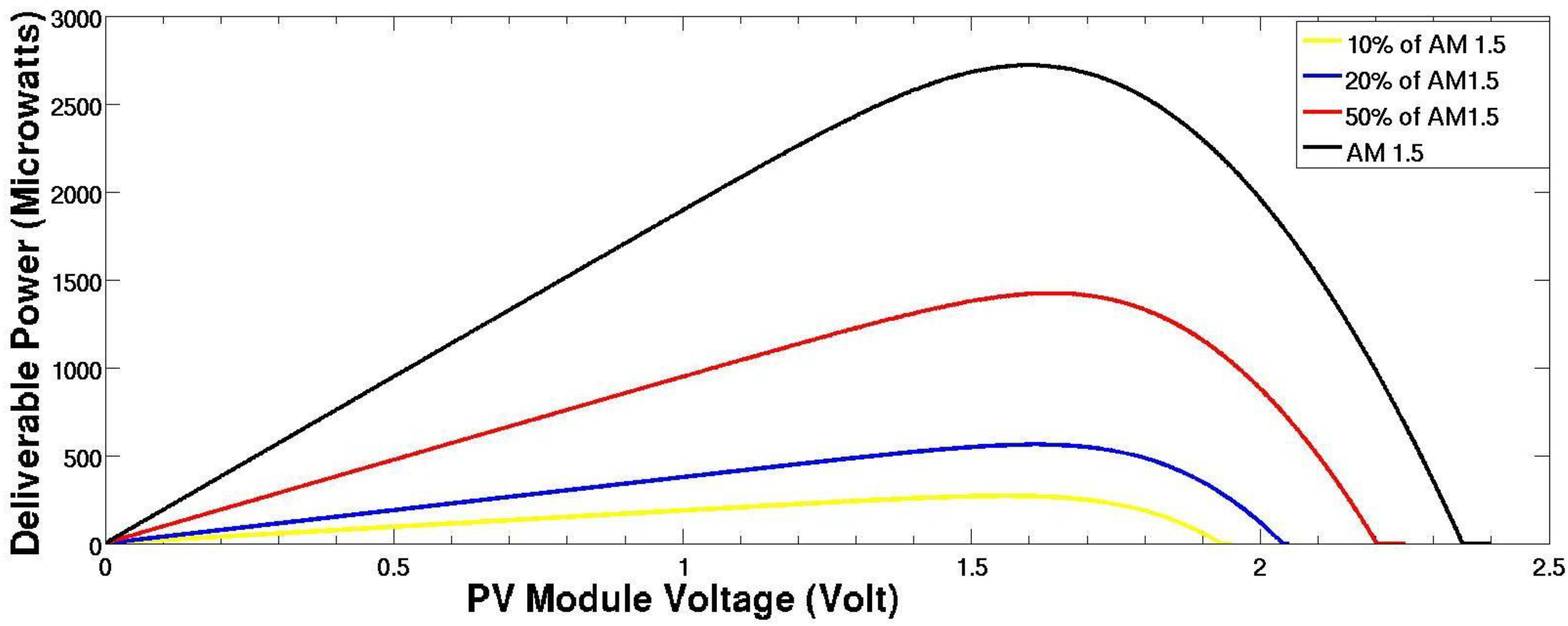
The block diagram of the target H2 gas sensor, including the required external components and the main blocks of the proposed solar energy harvester, is depicted in Figure 1. Four miniaturized nanowire solar cells have been connected in series to be used as the energy source. The main tasks of a solar energy harvester block are battery charging, battery management and energy management. The direct charging method proposed in [6] has been used for charging the target NiMH microbattery with very high efficiency. In this approach, battery voltage (Vbat) is compared with open circuit voltage of the PV module (Vpv) using a dynamic comparator, and if it is lower, the battery is connected to the PV module to store harvested energy. If Vpv drops below Vbat, the switch between Vpv and Vbat is kept turned off to avoid battery discharge through the PV module. In the direct charging method that has been deployed for solar energy harvesting, the maximum power point voltage (Vmpp) of the PV module should be close to the VEOC of the battery to achieve high efficiency. Although Pmpp and ISC of the PV module changes considerably in different lightning conditions, Voc and Vmpp of the PV module does not change significantly. In Figure 2, deliverable power of the PV module in different illumination levels has been simulated using the electrical model of the target PV module [12]. In AM1.5, solar intensity is almost 1 mW/mm2. Although, in 10% of AM1.5, deliverable power is reduced by roughly the factor of 10; Voc drops from 2.35 V to 1.95 V.
The second main task of the energy harvester circuit is battery management. As the charging current is limited by the PV module, the battery is charged in either standard or trickle charging modes, depending on the illumination conditions [2]. In trickle charging mode, the battery is charged by a small current, and it can be continuously charged after reaching VEOC. However, in standard charging mode, the battery charging should be stopped after reaching VEOC to avoid permanent damage to the battery. In addition, to avoid full discharge of the battery that reduces the cycle life of the battery, the battery should be disconnected from the sensor when it drops to VEOD. In order to avoid overdischarge or overcharge of the battery in standard charging mode, VEOC and VEOD voltage levels are detected by this circuit.
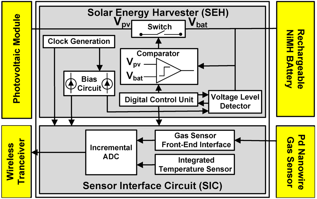
Figure 1.
Block diagram of the proposed hydrogen gas sensor.
Figure 1.
Block diagram of the proposed hydrogen gas sensor.

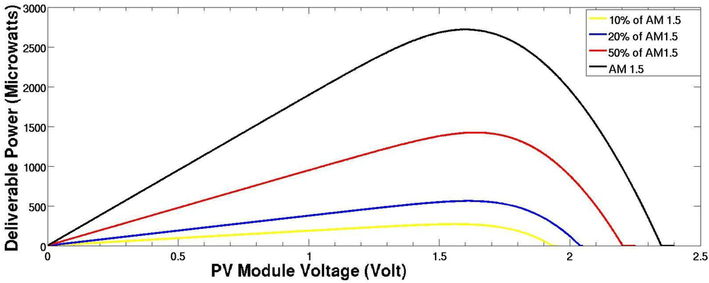
Figure 2.
Deliverable power of the photovoltaic (PV) module in different lightning conditions.
Figure 2.
Deliverable power of the photovoltaic (PV) module in different lightning conditions.
Finally, the last task of the energy harvester circuit is energy management. Since, under reduced light intensity, the power delivered by the PV module may be lower than the average power consumption of the sensor, the energy harvester circuit should reduce power consumption of the microsystem to avoid full discharge of the battery during this period. Under reduced light intensity, the microsystem continues its autonomous operation at a lower speed and with a lower duty cycle. The proposed energy harvester circuit reliably measures energy stored in the target battery and scales the power consumption of the microsystem up or down according to the measurement results. In order to reduce the power consumption and speed of digital circuits, operating frequency is scaled down and data transceiver is activated by a lower duty cycle. Bias currents are also scaled down to reduce power consumption and the speed of analog circuits. In order to reliably estimate the energy stored in the battery, battery voltage is measured when the battery is discharged by a high discharge current.
The PV module, with the total area of 28 mm2, can provide a maximum power Pmpp of 2.88 mW at its Vmpp in AM1.5 illumination [1]. However, as harvested solar energy may be as small as a few micro-watts under reduced light intensities, the power consumption of this circuit should not be higher than a few hundred nanowatts to have high efficiency during these periods. As neither Vpv nor Vbat changes rapidly, comparator and voltage level detector blocks are activated every few seconds to minimize average power consumption. This circuit consumes less than 350 nW, which is mainly due to the clock generator and digital control unit that are always active.
2.3. Sensor Interface Unit
Pd nanowire grid fabricated on a silicon wafer has been used for gas sensing. Each grid consists of 14 Pd nanowires, half of which are covered with a passivation layer to prevent hydrogen from reaching the nanowire [8]. These coated nanowires, which are only sensitive to temperature, have been used as reference nanowires, while the remaining nanowires, which are sensitive to both temperature and H2 concentration, have been used as sensing nanowires. This circuit measures the conductance change of the sensing nanowires in comparison to the reference nanowires. In addition to eliminating the effects of temperature by first order, the measurement is only sensitive to the ratio of conductance of nanowires, instead of their absolute values, and as a result, a higher accuracy is achievable. Although the temperature effect is eliminated by first order, there are still second order effects, as the temperature coefficient of nanowire resistance changes according to H2 concentration. In order to compensate this second order effect, temperature is measured using an integrated temperature sensor [9]. H2 sensing accuracy can be increased by incorporating the measured temperature during sensor calibration. An incremental analog to digital converter (ADC) [13] converts the measured temperature and H2 concentration to 12-bit digital values. Power consumption and conversion time of this ADC can be reconfigured according to the energy stored in the battery to match the amount of available power, resulting in an adaptive, autonomous sensor. The power management circuit dynamically reduces the operating frequency of digital circuits and the bias currents of analog circuits in this sensor interface circuit under reduced light intensity. However, ADC conversion time increases as a result.
2.4. Wireless Transceiver
Emerging wireless sensors that are powered by micro-power energy harvesting sources have more stringent energy requirements compared to traditional wireless sensors. Apart from minimizing total power consumption of the sensor, which is mainly achieved by duty cycling operation of the sensor, they should have low peak power and ultra-low standby current. Low peak power ensures that miniaturized batteries with limited peak discharge currents can be used to power up the circuit. Ultra-low standby current guarantees that the average power consumption of the sensor can be minimized by heavily duty cycling sensing and data transmission. The main factors impacting power consumption of a wireless transceiver are supply voltage, carrier frequency and receiver sensitivity. The power consumption of transceiver can be reduced by operating at lower supply voltages. Although most of the wireless transceivers work with at least 1.8 V supply voltage, ultra-low power wireless transceivers with sub-1.2 V voltage, such as TZ1053 [3] or ZL70250 [14], are more suited to our application, thanks to their lower power consumption during data transmission and reception. These transceivers operate at sub-1 GHz frequency bands and have much lower peak-power and standby power, compared to state-of-the-art 2.4 GHz transceivers.
The second important factor is the carrier frequency. Some of the factors that affect choice of carrier frequency are operation range, power consumption, transmission data rates and antenna size. Although 2.4 GHz protocols, such as Zigbee, have been used extensively for wireless sensing applications, sub-1 GHz wireless systems offer several advantages for ultra-low power, low data rate applications. These transceivers have less power consumption for the same operating range, thanks to reduced attenuation rates and blocking effects at lower frequencies. Besides requiring higher power for the same link budget, higher traffic in the 2.4 GHz frequency band increases the interference in this frequency band.
Finally, receiver sensitivity also affects the power efficiency. A narrower bandwidth creates higher receiver sensitivity and allows efficient operation at lower transmission rates. Overall, all radio circuits running at higher frequencies, including low-noise amplifiers, power amplifiers, mixers and synthesizers, need more current to achieve the same performance as lower frequencies.
Although these sub-1 GHz transceivers have some disadvantages, such as larger size of antennas and lower data rates, overall, they are more suited for our application. A higher data rate can improve the energy efficiency (energy per bit) of the transceiver for high bandwidth applications with large data payloads. In fact, overall power consumption of a wireless transceiver is not only a factor of physical layer items, such as radio architecture, carrier frequency and antenna choice, but is also a function of the amount of time that the radio needs to run in order to transport the payload data over the air. Transmission time depends on the data rate and the protocol overhead to establish and maintain the communication link. For example, a Zigbee transceiver that has a 250 kbps data rate can send 1 MB of data almost five-times faster than a TZ1053 that has a 50 kbps data rate. However, in ultra-low power applications, typically, data payloads are small and a 50 kbps data rate is more than enough. In addition, as standard protocols, such as Zigbee or Bluetooth, offer highly sophisticated link and network layers and have a large protocol overhead, they are not very efficient for sending small data payloads.
3. System Implementation
3.1. Solar Energy Harvester
The proposed energy harvester is based on the direct charging scheme [6], in which a dynamic comparator compares Vbat with Vpv in a timely manner. The dynamic comparator and required control signals can be seen in Figure 3.

Figure 3.
Circuit diagram of dynamic comparator.
Figure 3.
Circuit diagram of dynamic comparator.
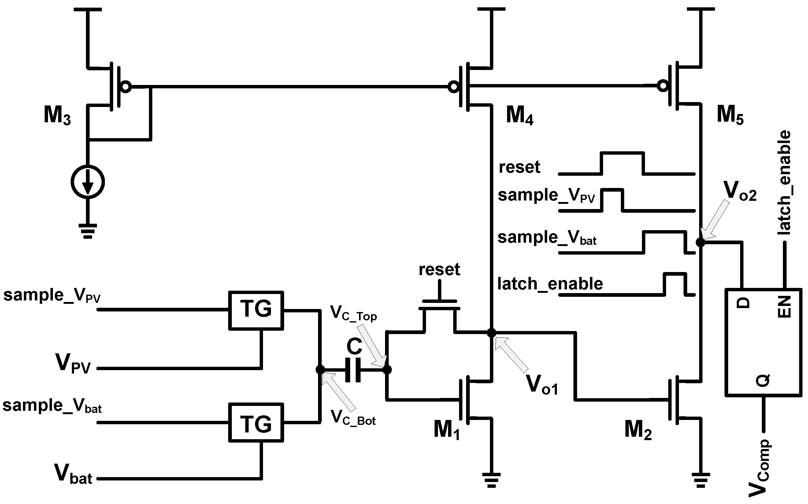
After turning off the switch between Vpv and Vbat, the first inverting gain stage gets reset by activating the reset control signal, to establish a common mode voltage of Vcm at the VC_Top node. Meanwhile, VC_Bot is connected to Vpv by activating the Sample_Vpv control signal, and the difference between Vpv and Vcm is sampled on the sampling capacitor. In the next step, by deactivating the reset and activating Sample_Vbat control signal, VC_Bot is connected to Vbat, and as a result, VC_Top changes to Vcm + (Vbat – Vpv). Outputs of the first and second gain stages (Vo1 and Vo2) change according to the new VC_Top, and Vo2 is latched and stored as VComp, by enabling the latch_enable control signal. If VComp gets 1, it means that Vbat is higher than Vpv, and the switch should be kept turned off to avoid battery discharge, but if VComp gets 0, the PV module starts to charge the battery by turning on the switch. After the switch is turned on, Vpv will follow Vbat during battery charging.
As the operating voltage of the PV module is determined by the battery, end-to-end efficiency from the PV module to the battery is reduced when battery voltage diverges from the Vmpp of the PV module during battery charging. Different maximum power point tracking (MPPT) strategies have been deployed in energy harvesting applications to maximize the amount of harvested energy. As the Vmpp of the PV module varies with incident light conditions, an efficient MPPT scheme ensures that the maximum power is extracted from a PV module at any given time. Many complex and accurate MPPT schemes have been investigated for large solar harvesting systems [15]; however, when the PV module is small and can only provide a few micro-watts under reduced light intensity, only low-overhead schemes that incur very little power overhead can be good candidates. In [16], several low-overhead MPPT approaches, including fractional open-circuit voltage (FOC), fractional short circuit current (FSC) and hill-climbing techniques, have been discussed that can be deployed in inductive and SC DC-DC converters. Although in direct charging Vpv always follows Vbat and no MPPT scheme can be deployed, nevertheless, it achieves even higher efficiency than competing SC and inductive DC-DC converters [6]. In addition, the die area is much smaller than SC and inductive DC-DC converters, as large passive components, such as pumping capacitors, or inductors have not been used in this architecture.
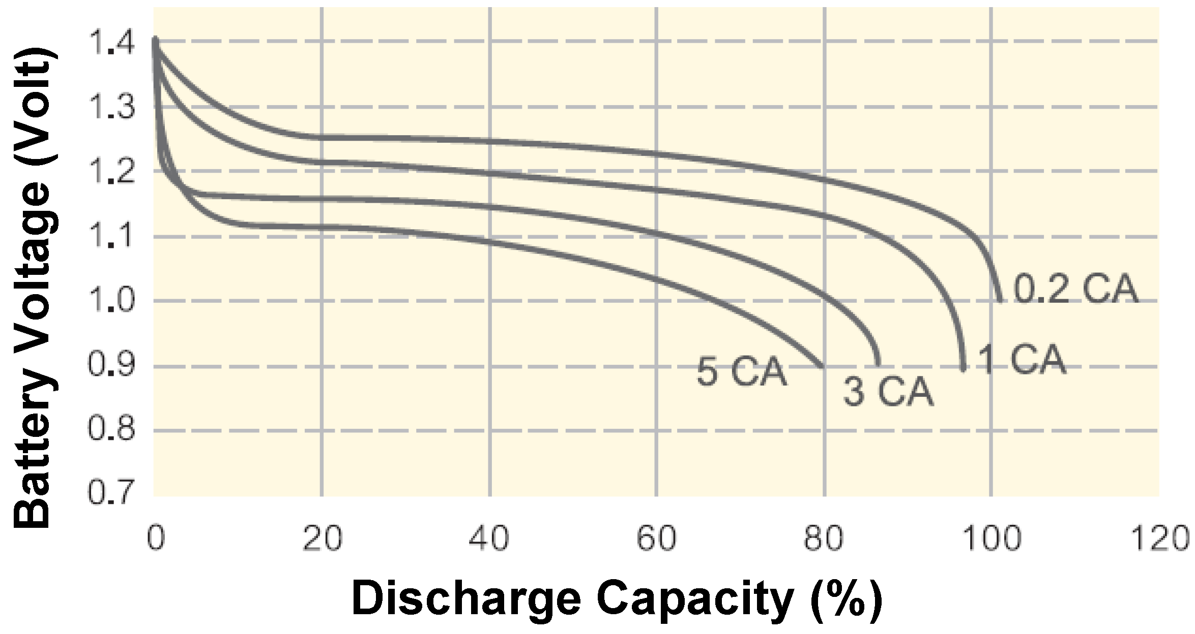
When the target V6HR NiMH microbattery is fully charged, the battery voltage is close to VEOC; as the battery is discharged by a low current, Vbat drops to its nominal value and remains almost constant, up to getting close to the fully discharged state. However, if the battery is discharged by a high current, as can be seen in the discharge curve of the battery in Figure 4 [2], Vbat drops immediately and voltage drop depends on the remaining charge of the battery. During wireless data transmission, the battery is discharged by a high current, close to 5 CA (C being the 1 hour charge or discharge current). As can be seen in Figure 4, if discharge capacity is less than 20%, Vbat is higher than 1.1 V during this period; however, if discharge capacity is higher than 20%, Vbat drops from 1.1 V down to 900 mV, depending on the remaining charge of the battery.
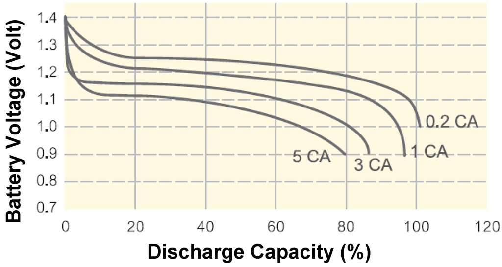
Figure 4.
Typical discharge curves of the target NiMH microbattery at room temperature [2].
Figure 4.
Typical discharge curves of the target NiMH microbattery at room temperature [2].
In our circuit, battery voltage is detected during this period to accurately estimate the energy stored in the battery. Depending on the detected Vbat, the power-performance of the integrated electronic circuits and operation duty cycle of the wireless transceiver are reconfigured to guarantee autonomous operation of the sensor. If Vbat is high enough, the sensor can operate at its highest performance: solar energy harvester and sensor interface circuits work at their highest speed, and measurement results are sent to the base station every 10 seconds. If Vbat is not high enough, the sensor interface circuit and wireless transceiver are activated with a lower duty cycle to minimize total power consumption of the sensor. If Vbat is close to VEOD, these blocks should get deactivated temporarily to avoid full discharge of the battery.
The voltage level detector (LD) in Figure 5 is used to determine the battery voltage level [6]. After circuit startup, battery voltage is checked to make sure that it is more than the end of discharge threshold voltage (VEOD) and can power up the circuit. If Vbat is less than VEOD, it means that the battery is fully discharged and cannot provide enough power for the electronic circuits. In this situation, the PV module continuously charges the battery by keeping the switch closed. As soon as Vbat passes VEOD, LD starts its normal operation, comparing Vbat with specified threshold voltages in a timely manner and updating the Vbat_level as a result. In order to generate a bandgap reference voltage, 25 substrate PNP transistors have been used as Q1 and Q2 in a common-centroid layout [6]. These transistors are biased with a 100 nA current source to generate VBE1 and VBE2 in non-overlapping Φ1 and Φ2 phases, and the SC circuit sums up VBE1 and (VBE1 – VBE2) with appropriate coefficients. When Vbat reaches VEOC, the switch between the PV module and the battery is turned off to avoid overcharge of the battery.
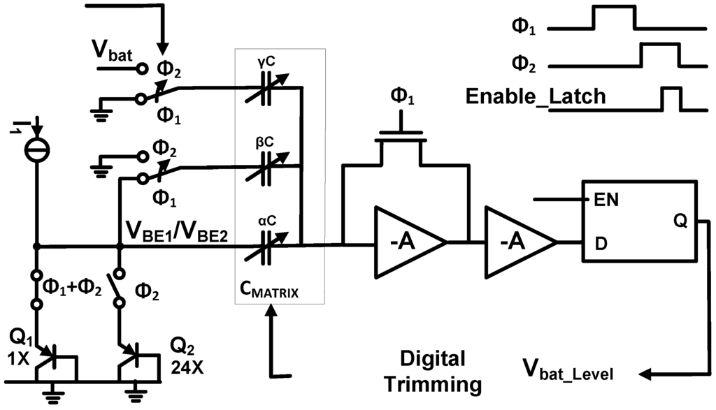
Figure 5.
Circuit diagram of voltage level detector.
Figure 5.
Circuit diagram of voltage level detector.

This SC circuit detects when Vbat passes the VL specified in Equation (1) by setting the Vbat_level output. By using a variable γC capacitor, different voltage levels between VEOD and VEOC can be detected to estimate the remaining charge of the battery. In Equation (1), α, β and γ coefficients are the ratios of tunable αC, βC and γC capacitors. These variable capacitors have been implemented using a matrix of 10 fF metal-insulator-metal (MIM) capacitors that have been used as unity capacitors.

As VBE1 is complementary to absolute temperature (CTAT) and (VBE1VBE2) is proportional to absolute temperature (PTAT), different CTAT, PTAT or temperature-independent reference voltages (Vref) can be built by proper selection of αC and βC capacitors. After that, by modifying the γC capacitor, target voltage levels can be detected. As can be seen in Table 2, by modifying βC and γC capacitors, different battery voltages, starting from VEOD of 0.9 V up to VEOC of 1.5 V, can be detected. In order to have a temperature-independent voltage reference, αC should be modified according to the selected βC capacitor. By detecting the battery voltage between 900 mV and 1.1 V, the remaining charge of the battery can be estimated according to the discharge curve of the battery in Figure 4.

Table 2.
Detected voltage levels in voltage level detector.
| Voltage Level (VL) | αC Capacitor | βC Capacitor | γC Capacitor |
|---|---|---|---|
| 907 mV (VEOD) | 170 fF | 1230 fF | 230 fF |
| 947 mV (VL0) | 170 fF | 1230 fF | 220 fF |
| 1002 mV (VL1) | 180 fF | 1300 fF | 220 fF |
| 1051 mV (VL2) | 180 fF | 1300 fF | 210 fF |
| 1104 mV (VL3) | 190 fF | 1370 fF | 210 fF |
| 1509 mV (VEOC) | 160 fF | 1160 fF | 130 fF |
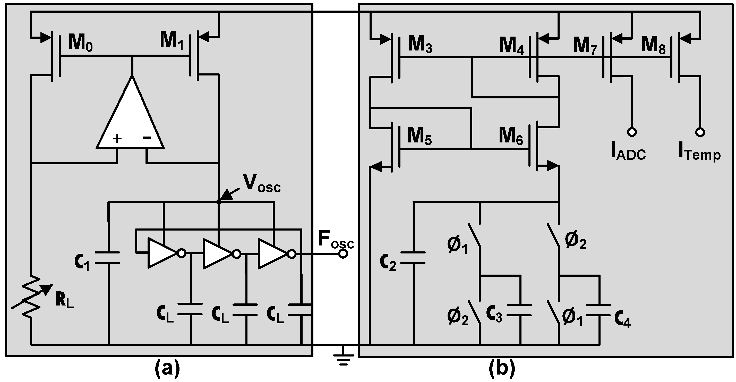
After measuring Vbat and estimating the energy stored in the battery, the operating frequency of digital circuits and bias currents of analog circuits are reconfigured according to the remaining charge of the battery. In the current-starved ring oscillator in Figure 6a, the frequency is determined by RL and CL and can be specified as Equation (2). In Equation (2), K1 is a constant value that depends on the number of inverter stages in the ring oscillator [17]. By using a digital resistive trimming network to modify RL, Fosc is reconfigured by an energy harvesting circuit, according to the measured Vbat. When Vbat is low, RL is increased to decrease Fosc. Four target operating frequencies have been considered, corresponding to four voltage levels that are detected by the LD block, ranging from 125 kHz, corresponding to VL0, to 1 MHz corresponding to VL3.

In addition to a fixed 10 nA beta-multiplier (BM) current reference that has been used to provide the required bias current for a solar energy harvester, a switched-capacitor beta-multiplier (SCBM) current source has been designed to generate frequency-proportional bias currents. In this circuit, which can be seen in Figure 6b, SC resistors have been used instead of regular resistors to generate frequency-proportional bias currents [18]. For example, IADC can be specified as in (3):


In Equation (3), K1 and K2 are constant values that depend on the ratio between the widths of transistors in Figure 6b. K1 depends on the ratio between M7 and M4, and K2 depends on the ratio between M5 and M6. The current ripple of Ibias is minimized by using a large decoupling capacitor, C2, and two complementary branches charging and discharging C3 and C4 capacitors in non-overlapping Ø1 and Ø2 clock phases with Fosc frequency [18]. As Fosc is determined by the oscillator, Ibias scales dynamically by changing the frequency of the oscillator. In addition, this current source can be easily deactivated by turning off the Ø1 and Ø2 clocks.
In ultra-low power analog circuits, such as the discrete time incremental ADC that has been used here, bias currents should be high enough to guarantee correct operation at the target operating frequency. Generated bias currents (IADC and ITemp) have been used for the sensor interface circuit. If Vbat is low, Fosc is decreased to reduce the power consumption of digital circuits in the ADC. When the system is operating at a lower frequency, lower bias currents can be used to reduce the power consumption of analog circuits in the sensor interface circuit. By using these frequency-proportional bias currents, power consumption of the sensor can be scaled down dynamically by reducing Fosc.

Figure 6.
(a) Reconfigurable current-starved ring oscillator; (b) switched-capacitor beta-multiplier (SCBM) current source.
Figure 6.
(a) Reconfigurable current-starved ring oscillator; (b) switched-capacitor beta-multiplier (SCBM) current source.
The digital control unit (DCU) activates the comparator and LD blocks in a timely manner, to check the charging status of battery. As neither Vbat nor Vpv change rapidly, these blocks are activated every few seconds to minimize their average power consumption. After activating each block, DCU generates the required control signals for related SC circuits. Standard complementary metal-oxide-semiconductor (CMOS) logic has been used to implement DCU. The power consumption of DCU is mainly determined by the low frequency 20-bits counter that activates the comparator and LD in a timely manner. Table 3 presents die area and power consumption of individual blocks, operating at 1 MHz as its highest clock frequency. As can be seen, the simulated total power consumption of the circuit is mainly determined by the clock generator, bias circuit and DCU blocks, which are always active. Although comparator and LD blocks consume considerable power during their active time, nevertheless, as they are activated every 10 seconds, their average power consumption is less than 1 nW. When Vbat is low, the average power consumption of the clock generator and DCU blocks is reduced by operating at a lower clock frequency. By reducing the operating clock frequency, the simulated power consumption of clock generator and DCU is reduced roughly linearly, reaching to 23 nW and 13 nW, respectively, at 125 kHz.

Table 3.
Die area and active power of main blocks in solar energy harvester circuit.
| Block | Die Area (µm2) | Active Power (nW) | Average Power (nW) | |
|---|---|---|---|---|
| Clock generator | 14,400 | 165 | 165 | |
| Digital control unit | 38,115 | 90 | 90 | |
| Bias circuit (10 nA) | 2,832 | 35 | 35 | |
| Comparator | 759 | 55 | <1 | |
| Level detector | 31,960 | 520 | <1 | |
| SCBM | 6,300 | 640 | <1 | |
3.2. Sensor Interface Circuit
The proposed sensor interface circuit is depicted in Figure 7. An incremental ADC [13] measures H2 concentration and temperature at different times. Individual Pd nanowires that have between 7 kΩ and 9 kΩ resistance should be biased, with a minimum bias voltage of 50 mV for 10 seconds. These nanowires have been represented by NWref and NWsense in Figure 7. The conductance of NWsense nanowires may change by 20% in comparison with NWref nanowires as H2 concentration varies from zero to 30% [7]. The voltage around the reference nanowire, VR = (V1 – V2), is used as the reference voltage, while the voltage of the sensing nanowire (V2) is used as the input voltage for the following incremental ADC in consecutive non-overlapping clock phases. This ADC can achieve 12 bits resolution by using 200 fF metal-insulator-metal (MIM) capacitors, as C3, C4 and C5, and a conventional two-stage amplifier with at least 75 dB gain for the integrator [9]. As a 1 MHz clock has been used for ADC and since this ADC needs 2N cycles for N-bits conversion, a 12-bit conversion takes nearly 4 ms. After finishing gas sensing, temperature is measured to further increase the accuracy of gas sensing using an integrated temperature sensor. In the proposed integrated temperature sensor, substrate PNP transistors have been used to generate proportional to absolute temperature (Vptat) and temperature-independent reference (Vref) voltages, and the ADC converts (Vptat/Vref) to a 12-bit digital value. In Figure 7, by using a 50 fF MIM capacitor as C1 and a 360 fF MIM capacitor as C2, a temperature-independent reference voltage of approximately 310 mV has been generated. Similar to gas sensing, n-bit digital representation of (Vptat/Vref) is stored in the ADC counter and sent to a wireless transceiver after temperature sensing. The accuracy of temperature sensing is mainly limited by mismatch between Q1 and Q2 and nonlinearity in temperature dependence of VBE1 and (VBE1VBE2). Although these errors can be minimized by using dynamic methods presented in [19] to reach ±0.1 °C accuracy, such power-consuming techniques are not needed here. The proposed low power temperature sensor can achieve ±1 °C accuracy by only calibrating C2 and ITemp at room temperature [9]. When the sensor interface circuit operates at a lower frequency, Q1 and Q2 transistors are biased with a lower ITemp bias current to reduce the average power consumption of the circuit.
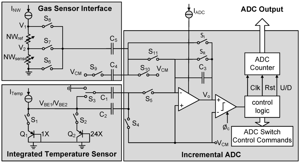
Figure 7.
Circuit diagram of the proposed sensor interface.
Figure 7.
Circuit diagram of the proposed sensor interface.

4. System Integration and Performance
The circuit has been implemented in a 0.18 µm CMOS process with 0.25 mm2 total area, as can be seen in the chip microphotograph in Figure 8. The main blocks, including the digital and analog blocks of solar energy harvester and sensor interface circuits, have been specified separately. When operating at 1 MHz, the whole circuit consumes almost 2.1 µW; while the average power consumption of the energy harvester is less than 350 nW. The wireless transceiver sends the measurement results for both temperature and H2 concentration to a base station every 15 seconds.
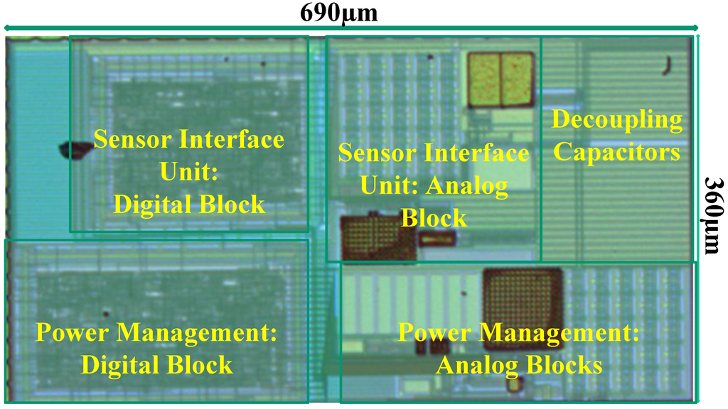
Figure 8.
Chip microphotograph of the whole microsystem.
Figure 8.
Chip microphotograph of the whole microsystem.

Table 4 presents measurement and simulation results for power consumption of the energy harvester and sensor interface circuits in different system operation modes. These operation modes have been defined according to the remaining charge of the battery, which is estimated accurately by detecting the battery voltage between 900 mV and 1.1 V during wireless data transmission, and the battery is discharged by a high current, close to 5 CA. Battery discharge capacity is determined according to the discharge curve of the battery shown in Figure 4. By using highly resistive poly resistors, total layout area has been decreased compared to [9]; however, as these embedded resistors are sensitive to process variations, absolute values are important for all resistors, including resistors that have been used in the beta multiplier current source, and oscillator are trimmed initially. If the battery gets discharged, a lower battery voltage is detected during 5 CA discharge and the system is switched to a lower clock frequency to decrease the average power consumption of the whole system. In SL2 and SL1 modes, the operating frequency is decreased to 500 kHz and 250 kHz, respectively. In SL0 mode, when the remaining charge of the battery is less than 25%, the circuit consumes less than 0.6 µW by operating at 125 kHz frequency instead of 1 MHz and using lower bias currents. The average power consumption of the energy harvester drops to less than 110 nW in SL0 mode. In addition, measurement results are sent every 120 seconds instead of every 15 seconds in SL3 mode, to further reduce the total average power consumption of the whole sensor.

Table 4.
System performance and power consumption in different system operation modes.
| Block | SL3 | SL2 | SL1 | SL0 | ||
|---|---|---|---|---|---|---|
| Detected Vbat during 5CA discharge (mV) | 1,104 | 1,051 | 1,002 | 947 | ||
| Battery discharge capacity (%) | <20% | <50% | <65% | <75% | ||
| Battery threshold voltage (V) | Measured | 1.114 | 1.055 | 1.003 | 0.955 | |
| Simulated | 1.122 | 1.063 | 1.010 | 0.962 | ||
| Clock frequency (kHz) | Measured | 950 | 488 | 249 | 127 | |
| Simulated | 980 | 502 | 257 | 132 | ||
| Time interval of sensing and data transmission (seconds) | 15 | 30 | 60 | 120 | ||
| Power consumption of clock generator (nW) | 165 | 85 | 44 | 23 | ||
| Power consumption of digital control unit (nW) | 90 | 46 | 24 | 13 | ||
| Average power consumption of energy harvester (nW) | Measured | 346 | 210 | 142 | 103 | |
| Simulated | 293 | 169 | 106 | 74 | ||
| Average power consumption of sensor interface circuit (nW) | Measured | 1730 | 1120 | 790 | 640 | |
| Simulated | 1360 | 870 | 625 | 500 | ||
| Average power consumption of the integrated circuit (nW) | 2076 | 1330 | 932 | 707 | ||
| Average current consumption of gas sensor bias circuit (µA) | 4.67 | 2.33 | 1.16 | 0.58 | ||
| Average current consumption of the wireless transceiver (µA) | 9.4 | 7.7 | 6.6 | 5.55 | ||
| Average current consumption of the complete system (µA) | 16 | 11 | 8.5 | 6.7 | ||
In order to estimate total power consumption of the sensor, the average power consumption of sensor biasing circuit and wireless transceiver should be calculated. Pd nanowires should be biased with a 7 µA bias current for 10 seconds, before measuring H2 concentration. TZ1053 consumes 5 µA during standby and consumes 3.3 mA during a period of 20 ms to send a sample with the minimum payload size of 55 bytes [3]. In SL3 mode, samples are sent every 15 seconds, and the average current consumption of Pd nanowire sensors and wireless transmission are 4.67 µA and 9.4 µA, respectively. By sending the samples every 120 seconds in SL0 mode, these values will be reduced to 0.58 µA and 5.6 µA, respectively. So, the total average current consumption of the whole sensor is less than 16 µA, operating at its highest performance in SL3 mode, and is reduced to less than 7 µA, operating in SL0 mode.
Four nanowire solar cells presented in [1] have been connected in series to provide an appropriate Vmpp voltage, close to the VEOC of the V6HR NiMH battery. The power delivered to the battery by the PV module can be simulated using the equivalent circuit model of the PV module. This PV module, with total area of 28 mm2, can provide a maximum power of 2.88 mW at its Vmpp under AM1.5 illumination level [1]. In order to evaluate autonomous operation of the sensor, end-to-end efficiency from the PV module to the battery has been simulated in different illumination levels. As can be seen in Table 5, even in 1% light intensity, the PV module delivers average power of 18.4 µW to the battery with 89.8% average efficiency. The power that can be delivered to the battery in 1% can be seen in Figure 9. When battery voltage is close to VEOD, 15.9 µW power is delivered to the battery with 76.8% efficiency. As in this situation, the system is operating in SL0 mode, its average power consumption is less than 8 µW and the battery gets charged. By increasing the battery voltage, efficiency is improved and more power is delivered to the battery. As a result, even in 1% light intensity, the harvested energy is enough for autonomous operation of the whole system. Meanwhile, as the whole sensor node consumes less than 16 µA for sensing and data transmission, the target 6 mAh battery can provide enough power for approximately 375 hours operation, even without energy harvesting.

Table 5.
Die area and active power of solar energy harvesting blocks.
| Illumination Level | Vmpp (V) | Pmpp (µW) | Pcharge (µW) | Efficiency |
|---|---|---|---|---|
| 100% of AM1.5 | 1.586 | 2,718 | 2,240.8 | 82% |
| 50% of AM1.5 | 1.622 | 1,422 | 1,127.3 | 79.2% |
| 20% of AM1.5 | 1.604 | 561.6 | 448.4 | 79.8% |
| 10% of AM1.5 | 1.549 | 269.5 | 221.4 | 82.1% |
| 1% of AM1.5 | 1.289 | 20.3 | 18.4 | 89.3% |
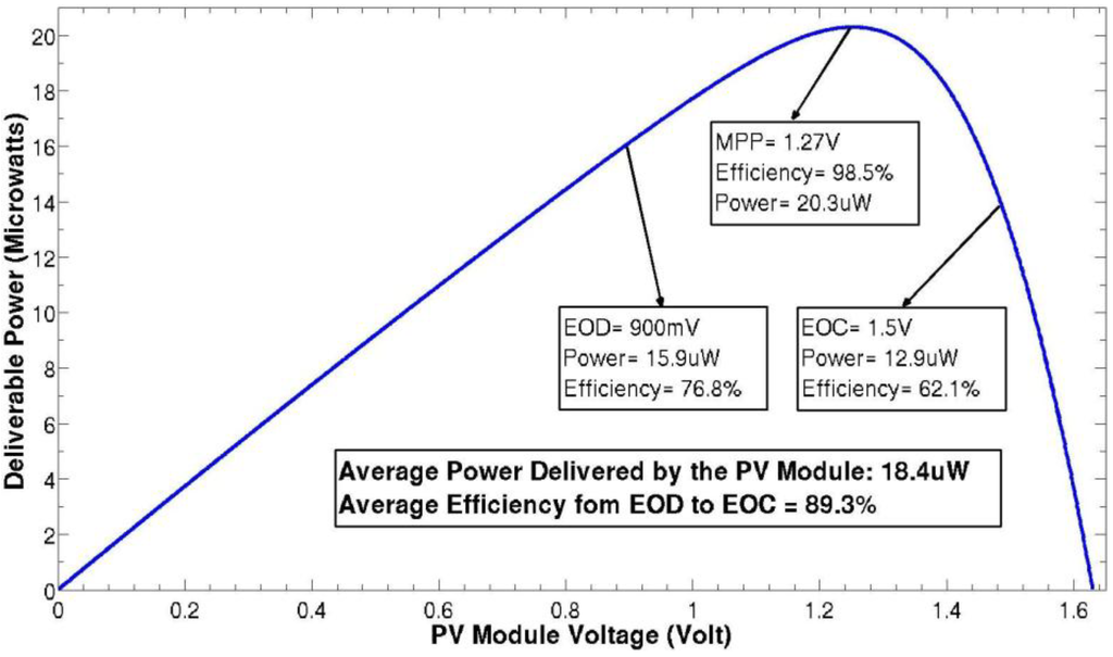
Figure 9.
Power delivered to the battery under simulated 1% of AM1.5 illumination.
Figure 9.
Power delivered to the battery under simulated 1% of AM1.5 illumination.
5. Conclusions
An ultra-low power energy-efficient solar energy harvesting and sensing microsystem has been proposed for wireless sensing applications. The circuit has been realized in a 0.18 µm CMOS process with only a 0.25 mm2 die area to measure both hydrogen concentration and temperature, using fully integrated solar energy harvesting and sensor interfacing circuits. An external wireless data transceiver is used to transmit the measurement results to a base station. Four nanowire solar cells have been connected in series, and the proposed area- and power-efficient energy harvester circuit stores the energy harvested from the PV module in a NiMH microbattery. In addition, this circuit scales the power consumption and performance of the sensor by reconfiguring the operating frequency, bias currents and time interval of sensing and data transmission to guarantee autonomous operation of the sensor. This circuit consumes only 2.1 µW when operating at its highest performance, which is further reduced to less than 0.7 µW when operating at its lowest speed. Simulation results show that even under reduced illumination, the harvested energy is enough for autonomous operation of the sensor.
Acknowledgments
This work is supported by European project SiNAPS under contract number 257856. The authors would like to thank Fritz Falk and Jia Goubin from the Institute of Photonic Technology, Jena (IPHT-Jena) for providing miniaturized nanowire solar cells.
References
- Jia, G.; Steglich, M.; Sill, I.; Falk, F. Core-shell heterojunction solar cells on silicon nanowire arrays. Sol. Energy Mater. Sol. Cells 2012, 96, 226–230. [Google Scholar] [CrossRef]
- Varra V6HR Datasheet. Available online: http://www.varta-microbattery.com (accessed on 3 December 2012).
- Toumaz TZ1053 Datasheet. Available online: http://www.toumaz.com/page.php?page=telran (accessed on 3 December 2012).
- Chen, G.; Ghaed, H.; Haque, R.; Wieckowski, M.; Yejoong, K.; Gyouho, K.; Fick, D.; Daeyeon, K.; Mingoo, S.; Wise, K.; Blaauw, D.; Sylvester, D. A Cubic-Millimeter Energy-Autonomous Wireless Intraocular Pressure Monitor. In Proceedings of IEEE International Solid-State Circuits Conference, San Francisco, CA, USA, 20–24 February 2011; pp. 310–312.
- Qiu, Y.; Liempd, C.V.; Veld, B.O.H.; Blanken, P.G.; Hoof, C.V. 5 μW-to-10 mW Input Power Range Inductive Boost Converter for Indoor Photovoltaic Energy Harvesting with Integrated Maximum Power Point Tracking Algorithm. In Proceedings of IEEE International Solid-State Circuits Conference, San Francisco, CA, USA, 20–24 February 2011; pp. 118–120.
- Khosro Pour, N.; Krummenacher, F.; Kayal, M. Fully integrated ultra-low power management system for micro-power solar energy harvesting applications. Electron. Lett. 2012, 48, 338–118. [Google Scholar] [CrossRef]
- Offermans, P.; Tong, H.D.; Van Rijn, C.J.M.; Merken, P.; Brongersma, S.H.; Crego-Calama, M. Ultralow-power hydrogen sensing with single palladium nanowires. Appl. Phys. Lett. 2009, 94, 223110–223113. [Google Scholar]
- Van der Bent, J.F.; van Rijn, C.J.M. Ultra low power temperature compensation method for palladium nanowire grid. Procedia Eng. 2010, 5, 184–187. [Google Scholar] [CrossRef] [Green Version]
- Pour, N.K.; Krummenacher, F.; Kayal, M. A Miniaturized Autonomous Microsystem For Hydrogen Gas Sensing Applications. In Proceedings of IEEE 10th International New Circuits and Systems Conference, Montreal, Canada, 17–20 June 2012; pp. 201–204.
- Cap-XX Co. Website. Available online: http://www.cap-xx.com (accessed on 3 December 2012).
- InfinitePowerSolutions Co. Website. Available online: http://www.infinitepowersolutions.com (accessed on 3 December 2012).
- Lu, C.; Raghunathan, V.; Roy, K. Micro-Scale Energy Harvesting: A System Design Perspective. In Proceedings of 15th Asia and South Pacific Design Automation Conference (ASP-DAC), Taipei, Taiwan, 18–21 January 2010; pp. 89–94.
- Markus, J.; Silva, J.; Temes, G.C. Theory and applications of incremental ΔΣ converters. IEEE Trans. Circuits Syst. 2004, 51, 678–690. [Google Scholar] [CrossRef]
- Zarlink ZL70250 Datasheet. Available online: http://www.zarlink.com/zarlink (accessed on 3 December 2012).
- Esram, E.; Chapman, P.L. Comparison of photovoltaic array maximum power point tracking techniques. IEEE Trans. Energy Conver. 2007, 22, 439–449. [Google Scholar] [CrossRef]
- Lu, C.; Raghunathan, V.; Roy, K. Maximum power point considerations in micro-scale solar energy harvesting systems. In Proceedings of IEEE International Symposium on Circuits and Systems (ISCAS), Paris, France, 30 May–2 June 2010; pp. 273–276.
- Pastre, M.; Krummenacher, F.; Kazanc, O.; Khosro Pour, N.; Pace, C.; Rigert, S.; Kayal, M. A solar battery charger with maximum power point tracking. In Proceedings of 18th IEEE International Conference on ElectronicsCircuits and Systems (ICECS), Beirut, Lebanon, 11–14 December 2011; pp. 394–397.
- Pastre, M.; Krummenacher, F.; Robortella, R.; Simon-Vermot, R.; Kayal, M. A fully integrated solar battery charger. In Proceedings of Joint IEEE North-East Workshop on Circuits and Systems and TAISA Conference, Toulouse, France, 28 June–1 July 2009; pp. 1–4.
- Pertijs, M.A.P.; Makinwa, K.A.A.; Huijsing, J.H. A CMOS smart temperature sensor with a 3σ inaccuracy of ±0.1 °C from −55 °C to 125 °C. IEEE J. Solid State Circuits 2005, 40, 2805–2815. [Google Scholar] [CrossRef]
© 2013 by the authors; licensee MDPI, Basel, Switzerland. This article is an open access article distributed under the terms and conditions of the Creative Commons Attribution license (http://creativecommons.org/licenses/by/3.0/).
