1. Introduction
Just as human beings acquire information about their environment through their senses and process such information using their brain, electronic systems perform such functions by means of sensors and processing digital devices such as microcontrollers (μC) or microprocessors (μP). Nowadays, such small but smart devices have become essential in many fields (industrial, automobiles, aircraft, medical devices, consumer electronics, home appliances, etc.) so that it is hard to imagine a society without them.
Figure 1(a) shows the classical block diagram of a sensor electronic interface [
1]. First of all, the sensor transforms a signal from a given energy domain (such as thermal, magnetic, mechanical, chemical or radiant) to the electrical domain by changing—for example—its electrical resistance or capacitance. Afterwards, the signal conditioning circuit, which generally relies on operational amplifiers (OpAmp), performs some or all of the following tasks in the analogue domain: sensor output-to-voltage conversion, amplification, filtering, linearization and/or demodulation. The resulting analogue signal is then digitized via an analogue-to-digital converter (ADC). Finally, a digital system (e.g., a μC) acquires, stores, processes, controls, communicates (to other devices or systems) and/or displays the digital value with information about the measurand.
Figure 1.
(a) Classical sensor electronic interface; (b) Direct interface circuit.
Figure 1.
(a) Classical sensor electronic interface; (b) Direct interface circuit.
Nowadays, several blocks, as shown in
Figure 1(a), can be embedded into the same integrated circuit (IC). There are commercially available ICs that integrate the processing digital system, the ADC and/or some signal conditioning circuit; for instance, MSC1210 from Texas Instruments (TI). There are also commercial ICs that integrate the sensor, its signal conditioning circuit and/or the ADC; for example, ADXL103 and ADXL312 accelerometers from Analog Devices; such chips are usually known as integrated smart sensors [
2]. Other commercial ICs integrate the required signal conditioning circuit and the ADC to measure a specific type of sensor; for instance, ADS1232 from TI for bridge-type resistive sensors and AD7745 from Analog Devices for single and differential capacitive sensors.
For some sensors, however, the block diagram in
Figure 1(a) can be simplified to that shown in
Figure 1(b) [
3], where the sensor is directly connected to the digital system without using either the signal conditioning circuit or the ADC; these circuits were initially proposed in application notes of μC’s manufacturers [
4,
5,
6]. In such a circuit topology (so-called direct interface circuit), the μC appropriately excites the analogue sensor to get a signal (usually, a time-modulated signal) that can be directly measured in the digital domain, for instance, using an embedded digital timer; such output signals are also known as quasi digital since the analogue information (e.g., period or time interval) can be directly measured by a digital system. In comparison with the sensor electronic interface shown in
Figure 1(a), a direct interface circuit is simpler and needs less components; actually, it just needs a common low-cost general-purpose 8-bit μC. Therefore, a direct interface circuit has advantages in terms of cost, physical space and power consumption, which is of major interest, for instance, in battery-powered measurement systems such as autonomous sensors. Furthermore, as will be shown along this paper, the performance of such circuits is quite remarkable taking into account their simplicity.
This paper reviews most of the work carried out about direct interface circuits and is organized as follows.
Section 2 describes the operating principle of such circuits.
Section 3 and
Section 4 explain how these circuits can be used to measure different topologies of resistive and capacitive sensors, respectively, and then discuss their performance.
Section 5 deals with the power consumption and proposes some design guidelines to reduce the current consumption. Finally,
Section 6 takes some conclusions and forecasts the future research work about this topic.
2. Operating Principle
Two measurement methods have been proposed so far to build the direct interface circuit shown in
Figure 1(b):
Direct interfaces based on a RC circuit [
3], where the μC measures the time interval needed to charge (or discharge) a capacitance
C to a given threshold voltage through a resistance
R; this method has been applied to measure resistive and capacitive sensors.
Direct interfaces based on charge transfer [
7,
8], where the μC counts the number of charge-transfer cycles needed to charge a reference capacitor to a given threshold voltage via a capacitive sensor; this method has been applied only to measure capacitive sensors.
Most of the research work about direct interfaces has been focused on those based on RC circuits, whose basics are explained by means of
Figure 2.
Figure 2.
(a) RC circuit; (b) Charging process; (c) Discharging process.
Figure 2.
(a) RC circuit; (b) Charging process; (c) Discharging process.
If
C is initially discharged and a step of amplitude
V1 is applied at the input, the output voltage is [see
Figure 2(b)]:
and the time required to charge
C from 0 to a given high threshold voltage (
VTH) is:
which is proportional to
R and
C. On the other hand, if
C is already charged to
V1 and a step towards ground is applied at the input, the output voltage is [see
Figure 2(c)]:
and the time needed to discharge
C from
V1 to a given low threshold voltage (
VTL) is:
which again is proportional to
R and
C. According to (4), if
C,
V1 and
VTL are known and
Td is measured, then the resistance of the RC circuit could be estimated by
R =
Td/(
Cln(
V1/
VTL)).
The RC circuit in
Figure 2(a) can be directly connected to a μC using the circuit topologies shown in
Figure 3(a) and
Figure 4(a). In
Figure 3(a),
R has been replaced by
Rx (
i.e., a resistive sensor) and
C by
Cd (
i.e., a capacitor whose nominal value is known), whereas in
Figure 4(a),
C has been replaced by
Cx (
i.e., a capacitive sensor) and
R by
Rd (
i.e., a resistor whose nominal value is known). Pins 1 and P are two input/output digital port pins. Pin 1, which is in charge of monitoring the exponential charging or discharging voltage, usually includes a Schmitt trigger (ST) buffer (with two threshold voltages) and should be associated to an external interrupt or a capture module. The circuits in
Figure 3(a) and
Figure 4(a) can measure either the charging time or the discharging time of the RC circuit, but the measurement of the latter is more recommended since it has lower variability. This is because the discharging-time measurement uses the low threshold voltage (
VTL) of the ST buffer, which is less noisy [
9] than the high threshold voltage (
VTH) used for the charging-time measurement.
Figure 3.
(a) Basic direct interface circuit for a resistive sensor (Rx); (b) Pin configuration during the charging stage; (c) Pin configuration during the discharging stage.
Figure 3.
(a) Basic direct interface circuit for a resistive sensor (Rx); (b) Pin configuration during the charging stage; (c) Pin configuration during the discharging stage.
Figure 4.
(a) Basic direct interface circuit for a capacitive sensor (Cx); (b) Pin configuration during the charging stage; (c) Pin configuration during the discharging stage.
Figure 4.
(a) Basic direct interface circuit for a capacitive sensor (Cx); (b) Pin configuration during the charging stage; (c) Pin configuration during the discharging stage.
The circuit in
Figure 3(a), which is for the measurement of resistive sensors, involves two operation stages: charging stage, and discharging and measurement stage. During the charging stage [see
Figure 3(b)], Pin 1 is set as an output providing a digital “1”, whereas Pin P is set as an input offering high impedance (HZ). Therefore, the capacitor
Cd is quickly charged to the analogue output voltage (
V1) corresponding to a digital “1”, which is generally equal to the supply voltage (
VDD). During the discharging and measurement stage [see
Figure 3(c)], Pin 1 is set as a HZ input and Pin P is set as an output providing a digital “0” and, consequently,
Cd is discharged towards ground through
Rx while the embedded timer measures the time interval required to do so; such a measurement is carried out using a high-frequency oscillator (with a period
TS) as a reference. When the exponential discharging voltage crosses
VTL, the timer is read and a digital number proportional to
Rx [see Equation (4)] is achieved. The resulting waveform of the voltage across
Cd is similar to that shown in
Figure 2(c).
For the measurement of a capacitive sensor (
Cx), it is recommended to swap the position of the resistance and the capacitance, as shown in
Figure 4(a), but again two operation stages are required. During the charging stage [see
Figure 4(b)], both pins are set as an output: Pin 1 provides a digital “1”, whereas Pin P provides a digital “0”. Therefore,
Cx is rapidly charged to
V1. During the discharging and measurement stage [see
Figure 4(c)], Pin 1 is set as a HZ input and Pin P does not change its state and, consequently,
Cx is discharged towards ground through the resistor
Rd while the timer is running. When the voltage-threshold crossing is detected [see
Figure 2(c)], the timer is read and a digital number proportional to
Cx [see Equation (4)] is achieved.
5. Current Consumption
For those applications in which the sensor is not read continuously but periodically (
i.e., every
TT seconds), the average current consumption of a direct interface circuit is
where
Iact is the average current consumption in active mode (
i.e., when the μC is working to perform the measurement),
Tact is the time interval required to complete one measurement in active mode,
N is the number of times that the measurement is repeated in active mode to average
N measurements,
Isleep is the current consumption of the μC in sleep (or standby) mode,
Tsleep is the time interval in which the μC is in sleep mode, and
TT =
N·Tact +
Tsleep. The value of
Isleep specifically depends on the low-power features of the μC, but it is generally smaller than 1 μA (even it can be smaller than 100 nA). On the other hand, the value of
Iact clearly depends on the configuration of the resources embedded into the μC during the measurement. To reduce the current consumption, it is advisable to set the CPU (Central Processing Unit) and the timer as indicated in
Table 10 [
29]; the rest of peripherals should be switched off. In the charging stage, the charging time should be controlled by the CPU running at low frequency (e.g., tens or hundreds of kHz); two remarks are as follows: (i) most of the current μCs have a prescaler to divide the master clock frequency, and (ii) a low-accuracy charging time (due to a low-frequency clock) is not a problem at all since the information is in the discharging time. In the discharging stage, the discharging time should be measured by the timer running at high frequency (e.g., units or tens of MHz) to have a good resolution, whereas the CPU should be off whenever this does not stop the operation of the interrupt system and the timer. In the processing stage, the CPU should run at high frequency (e.g., units or tens of MHz) to compute as fast as possible the resistance or capacitance of the sensor by means of, for example, (5) or (8).
Table 10.
Proposed state (on/off) and running frequency of the CPU and the embedded timer for each stage of the measurement.
Table 10.
Proposed state (on/off) and running frequency of the CPU and the embedded timer for each stage of the measurement.
| Stage | CPU | Timer |
|---|
| State | Frequency | State | Frequency |
|---|
| Charging | on | low | off | - |
| Discharging | off | - | on | high |
| Processing | on | high | off | - |
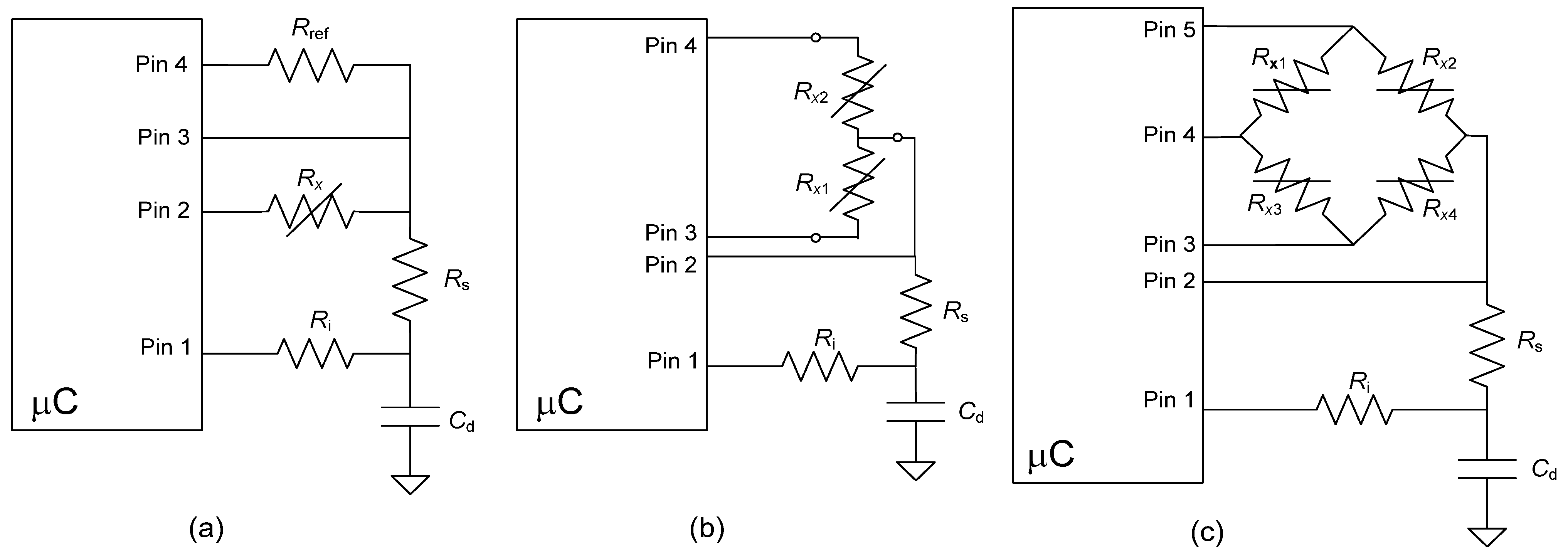
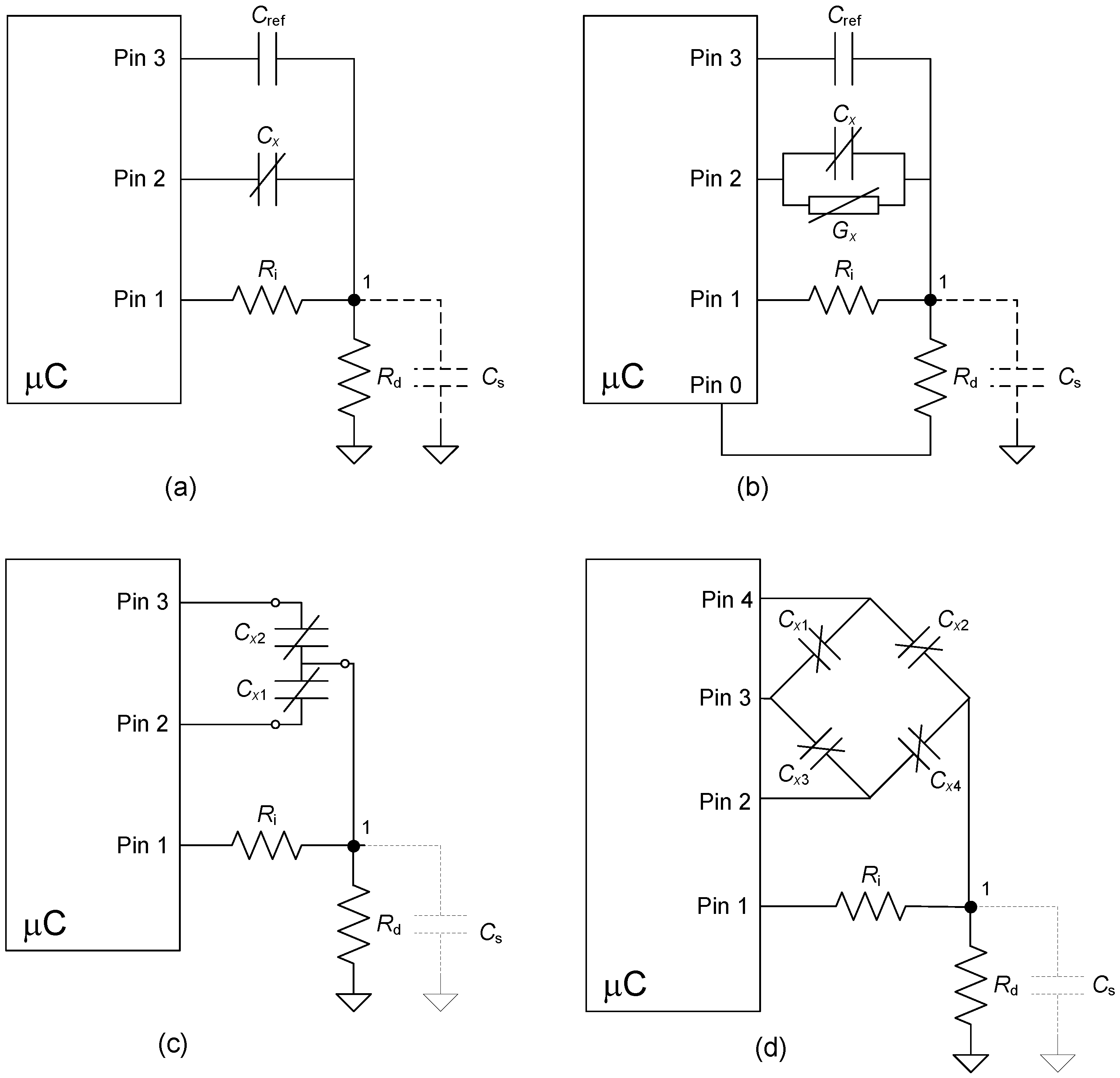
The average current consumption in active mode in measurements involving three charging stages, three discharging stages and one processing stage (as happens, for example, in the direct interface circuits shown in
Figure 5(a) and
Figure 6(a)) can be estimated by [
29]
where
C is the capacitance being charged [
i.e.,
Cd in
Figure 5(a) and
Cx in
Figure 6(a)],
Tc is the time interval required to charge
C,
Td is the discharging time to be measured,
Tp is the time interval required to process the discharging times, and
Iint1,
Iint2 and
Iint3 are the average current consumed by the internal electronics of the μC during the charging, discharging and processing stages, respectively. Note that in Equation (14)
Td is assumed to be the same for the three measurements; this assumption does not make sense in terms of the result obtained from (5) or (8), but it does in terms of current consumption analysis. According to (14), the current consumed by the internal electronics of the μC plays an important role on the overall current consumption. Furthermore, the value of
Iint1,
Iint2 and
Iint3 clearly depends on the supply voltage (
VDD) and operating frequency (
fclk) of the μC.
Table 11 shows, for example, some experimental values of such currents for an AVR μC running at different operating conditions when the configuration proposed in
Table 10 is applied.
Table 11.
Experimental values of average current consumed by the internal electronics of an AVR μC [
29].
Table 11.
Experimental values of average current consumed by the internal electronics of an AVR μC [29].
| | 3 V–4 MHz | 5 V–20 MHz |
|---|
| Iint1(1) (μA) | 61 | 472 |
| Iint2(2) (mA) | 0.43 | 4.13 |
| Iint3(3) (mA) | 1.51 | 11.79 |
Direct interface circuits for capacitive sensors are expected to be less power demanding than those for resistive sensors. This is because the first two components in Equation (14), which correspond to the charging stages, are almost negligible when measuring capacitive sensors in the picofarad range or smaller. Actually, the current consumption in active mode of direct interface circuits for capacitive sensors is equal, in a first approximation, to
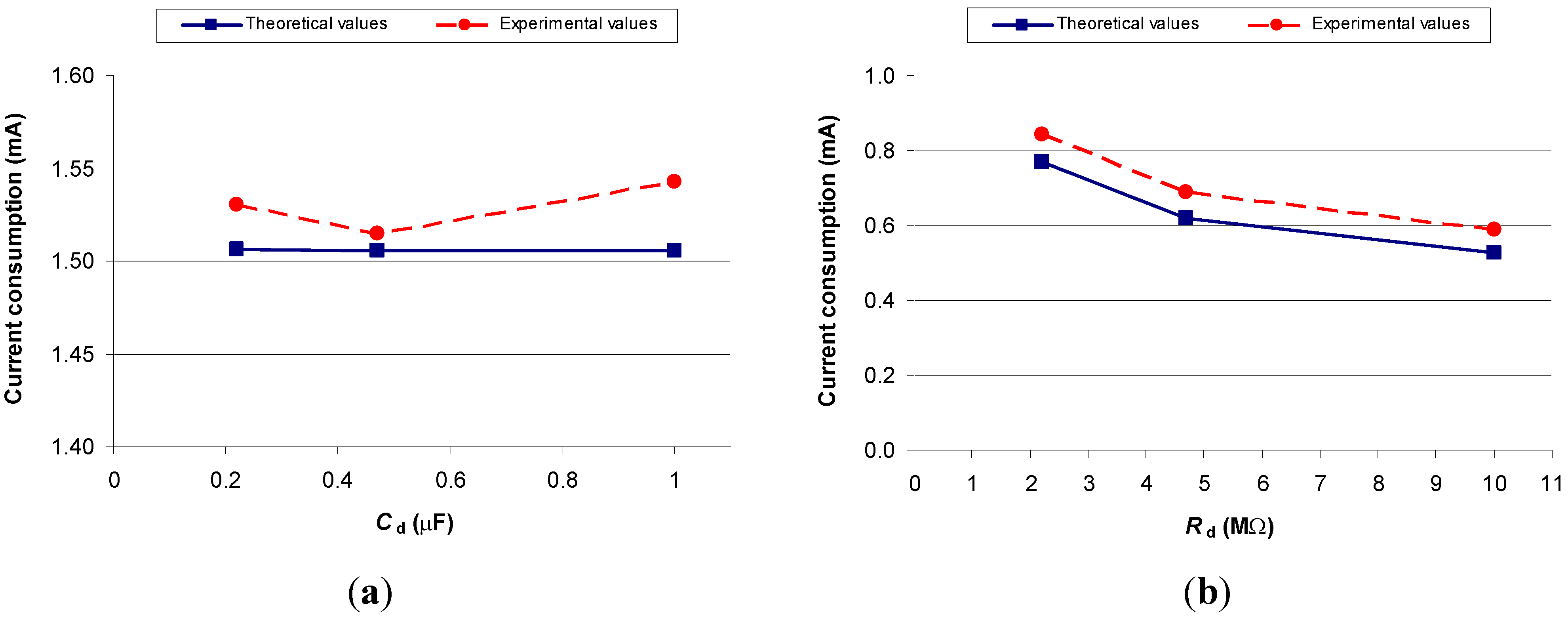
Iint2. Experimental tests carried out at 3 V – 4 MHz show that the current consumption when measuring capacitances (177 pF) is about 2–3 smaller than that when measuring resistances (1 kΩ), as shown in
Figure 7. In terms of measuring time and energy, a complete measurement of a 1-kΩ resistive sensor requires 1.6 ms and 7 μJ for
Cd = 220 nF, and 5.8 ms and 27 μJ for
Cd = 1 μF.
Figure 7.
Theoretical and experimental values of current consumption in active mode (
Iact) at 3 V – 4 MHz for (
a) the circuit in
Figure 5(a) when measuring a 1-kΩ resistive sensor, and (
b) the circuit in
Figure 6(a) when measuring a 177-pF capacitive sensor.
Figure 7.
Theoretical and experimental values of current consumption in active mode (
Iact) at 3 V – 4 MHz for (
a) the circuit in
Figure 5(a) when measuring a 1-kΩ resistive sensor, and (
b) the circuit in
Figure 6(a) when measuring a 177-pF capacitive sensor.
6. Conclusions and Outlook
Direct interface circuits are able to measure different topologies of resistive and capacitive sensors just using a common low-cost general-purpose 8-bit μC with an embedded digital timer but without any on-chip ADC, OpAmp or analogue comparator. In spite of their simplicity and low cost, these circuits perform remarkably and therefore they could be very attractive for medium-accuracy, medium-resolution applications. Note, however, that such a satisfactory performance is to be expected when measuring resistive sensors in the kiloohm range and capacitive sensors in the picofarad range. The measurement of low-value resistive sensors (say, lower than 100 Ω) is feasible, but the discharging-time measurement would suffer from a significant offset effect due to Rs, whereas the measurement of high-value resistive sensors (say, higher than 10 MΩ) could be affected by the parasitic resistance of the input port pins of the μC. On the other hand, the measurement of capacitive sensors with a nominal capacitance smaller than 1 pF seems impracticable because of the high effects of the parasitic capacitances of the input port pins of the μC. Direct interface circuits implemented with different commercial μCs from different manufacturers show similar results and, therefore, the design of such circuits does not depend on any specific device or integrated circuit from any manufacturer. A measuring time of about units or tens of millisecond can be a limitation of such circuits if the quantity to be measured changes quite fast.
The field of direct interface circuits is still under research and many interesting ideas could be developed in the near future. From the author’s point of view, future work on direct interface circuits could be focused on the following two directions:
(a) Applications: Many measurement systems based on resistive and capacitive sensors, but especially those intended for low-cost low-power applications, could benefit from the advantages of direct interface circuits. In fact, recently, such circuits have been proposed to measure low-power magnetic sensors for vehicle detection [
30], low-power gas sensors [
19] and low-cost low-power RH sensors to be integrated into RFID labels [
27].
(b) Measurement of other types of sensor: Most of the research work done so far on direct interface circuits has been focused on measuring resistive and capacitive sensors, but the direct measurement of other types of sensor is also of interest. For instance, the measurement of voltage-output sensors [
31], current-output sensors [
32] and impedance sensors [
33] has been proposed very recently.


