1. Introduction
As mobile devices become heavily energy constrained, the need for ultra low power circuits has emerged. In order to reduce energy consumption, voltage supplies are scaled down to take advantage of quadratic energy savings. The sub-threshold region (V
DD < V
T) has been shown by [
1] to minimize energy per operation. Sub-threshold systems require Static Random Access Memory (SRAM) for storing data at these low voltages. The problem is that while logic has been shown to easily scale into the sub-threshold region, the traditional 6T SRAM bitcell becomes unreliable at voltages below 700 mV due to process variations and decreased device drive strength [
2]. SRAM devices are typically minimum sized, which further compounds this problem. As the capacity of SRAM arrays continues to increase, the stability (typically measured in terms of Static Noise Margin (SNM) [
3]) of the worst case bitcell degrades. Therefore, in order for the minimum operating voltage (V
MIN) of SRAMs to enter the sub-threshold regime, more robust bitcell designs or assist methods must be used.
One possible solution to this problem is to design a more robust bitcell topology capable of larger read and write margins. The downside to this strategy is that adding more transistors to the bitcell increases the total area of the array. The second strategy is to use various assist methods [
4,
5,
6,
7,
8,
9,
10,
11,
12,
13] to make the cell easier to read and write. This method also results in a smaller area overhead and may require multiple voltage sources. In this work we will analyze different bitcell topologies and assist methods to determine which is the most effective at reducing SRAM V
MIN. In
Section 2, we will introduce a variety of sub-threshold bitcell topologies and explain the pros and cons of each. In
Section 3 and
Section 4 we will present an overview of read and write assist methods, and explain how each method can be used to improve margins.
Section 5 will present the results from a test chip, and
Section 6 will conclude.
2. Introduction of Sub-Threshold Bitcell Topologies
In a sub-threshold circuit, the supply voltage (V
DD) is set below the threshold voltage (V
T) of the transistors. This reduction in V
DD results in a quadratic reduction in switching power. In addition, it reduces leakage power, which is especially important for SRAMs that contain thousands or millions of bitcells. The main limitations of sub-threshold circuits are their sensitivity to variation and slow speed. In the sub-threshold region, transistor currents vary exponentially with V
T. This makes designing ratioed circuits such as SRAMs nearly impossible [
14]. Another problem is that the I
ON/I
OFF current ratio is reduced, which can lead to read access failures on bitlines with excessive leakage. In order to combat these problems, new bitcell topologies have been introduced and are described below.
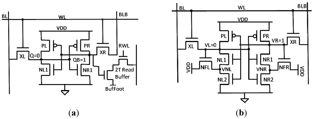
The 8T bitcell [
15] shown in
Figure 1a adds a two transistor read buffer to the conventional 6T bitcell in order to prevent the data from being disturbed during a read. In a normal read operation, the bitlines are precharged and the WL is pulsed high, causing the bitcell to discharge one of the bitlines. The problem with this is that if the node storing a “0” rises above the switching threshold of right inverter (
Figure 1a), then the cell could unintentionally flip. The 8T cell solves this problem by decoupling the data from the read operation; therefore the read SNM becomes the hold SNM. One weakness of this bitcell is that it still suffers from half-select instability, which occurs during a write when an unselected cell is read like a traditional 6T bitcell. Currently the best method to solve this problem in a bit interleaved architecture is by using a read before write scheme. In this method the entire row is read and then the data is written back into the unselected cells at the same time that new data is written to the selected cells.
Figure 1.
(
a) 8T bitcell with read buffer [
15]; (
b) 10T Schmitt Trigger inverter bitcell [
16].
Figure 1.
(
a) 8T bitcell with read buffer [
15]; (
b) 10T Schmitt Trigger inverter bitcell [
16].
The 10T bitcell [
16] (
Figure 1b) uses Schmitt Trigger (ST) inverters to help improve the read static noise margin (RSNM). The NR2/NFR feedback transistors weaken the pull down network when VR is high, increasing the switching threshold of the right inverter. This means that the VL node would have to pull up much higher during a read in order to flip the cell, resulting in higher read stability. This bitcell has been shown by [
16] to have 1.56× higher read SNM compared to the conventional 6T bitcell. The downside to this topology is that the four extra transistors result in a 33% area penalty compared to the 6T bitcell.
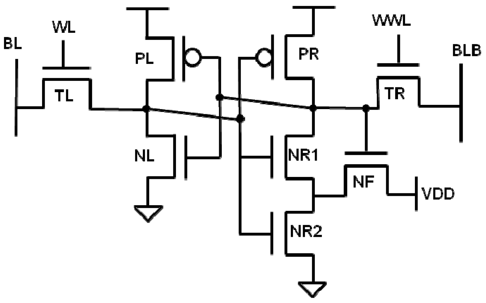
We propose an 8T asymmetric Schmitt Trigger bitcell (
Figure 2). This bitcell uses single-ended reading and asymmetric inverters, similar to the asymmetric 5T bitcell in [
17] to improve read margin. By using an asymmetrical design, the trip point of the ST inverter is increased, resulting in higher read stability. Because the 5T bitcell has only one access transistor, write assist methods must be used when trying to write a ‘1’ into the bitcell. The advantage that this design has over the 5T bitcell is that it is written like a traditional 6T bitcell, which eliminates the need for write assist methods. The WL is pulsed high during both a read and write, and the WWL is only pulsed high during a write. In simulation (
Figure 3) this bitcell achieves 86% higher RSNM than the 6T cell and 19% higher RSNM than the 10T ST bitcell with no V
T variation added.
Figure 2.
The 8T asymmetric ST bitcell schematic.
Figure 2.
The 8T asymmetric ST bitcell schematic.
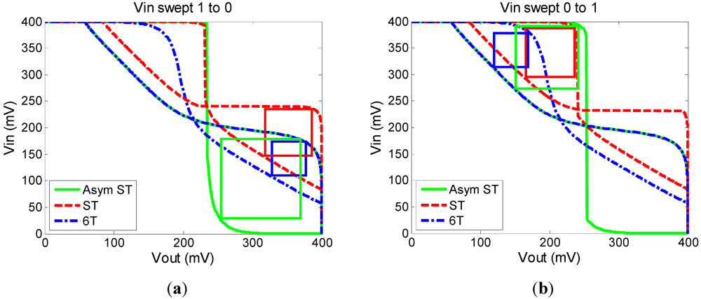
Figure 3.
Read butterfly curves for the asymmetric ST, ST and 6T bitcells. (a) shows the input swept from 1 to 0; (b) shows the input swept from 0 to 1.
Figure 3.
Read butterfly curves for the asymmetric ST, ST and 6T bitcells. (a) shows the input swept from 1 to 0; (b) shows the input swept from 0 to 1.
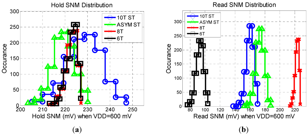
In
Figure 4, we compare statistic distributions of the read and hold static noise margins for each of the bitcells. The average hold static noise margin (HSNM) of the 6T and 8T bitcells is 222 mV, with the 10T ST slightly higher at 226 mV and the asymmetric ST slightly lower at 218 mV. However it is interesting to note that the standard deviation of the HSNM is 2.5 mV for 6T and 8T bitcells, 5.0 mV for the asymmetric ST, and 7.8 mV for the 10T ST bitcell. Therefore as the number of bitcells increases, the HSNM of the worst case bitcell in the 10T ST array will be lower compared to the other arrays. The average read static noise margin (RSNM) of the asymmetric ST is 88% higher than the 6T and 8% higher than the 10T ST. The 8T read distribution is the same as the hold distribution since the data is decoupled from the read operation. This assumes that the architecture of the 8T array does not interleave bits, or that a read before write scheme is implemented.
Figure 4.
(a) Hold and (b) Read static noise margin distributions for a 1000 point MC sweep.
Figure 4.
(a) Hold and (b) Read static noise margin distributions for a 1000 point MC sweep.
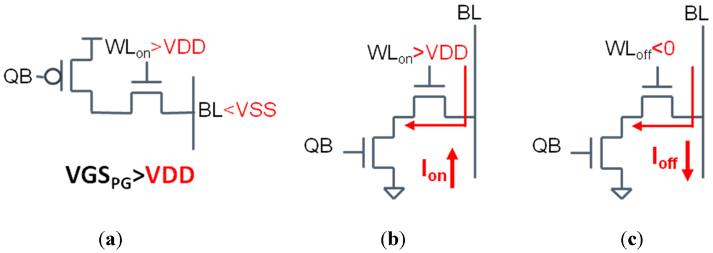
4. Read Assist Methods
Read failures can occurs in two ways. The first is that the bitcell is flipped during a read operation (referred to as read failure). This occurs when the XL and NL1 transistors (
Figure 1) are sinking the large amount of charge from the highly capacitive BL, and the Q node rises above the trip point of the right inverter. In order to increase read stability, the pull-down transistor is made stronger than the pass-gate. The second type of read failure occurs when the voltage difference between the BL and BLB is not large enough for the sense amp to determine the correct value (referred to as read access). This happens in sub-threshold especially due to the BL leakage current in unaccessed cells causing the BL voltage to droop. Because the I
ON/I
OFF ratio is reduced in sub-threshold, it is feasible for the leakage current through the unaccessed rows to pull the BL low at the same rate that the on current is pulling BLB low. This leakage current can be reduced by having less bitcells sharing the same bitline or by using one of the assist methods discussed below.
Figure 5.
(a) Increasing the pass-gate VGS allows for easier writing of the bitcell; (b,c) boosting the on current and reducing off current improves read access.
Figure 5.
(a) Increasing the pass-gate VGS allows for easier writing of the bitcell; (b,c) boosting the on current and reducing off current improves read access.
There are two goals involved in read assist methods. The first is to improve the stability of the cross-coupled inverters during the read by either raising the bitcell V
DD or reducing its V
SS [
4,
5,
7,
8,
9,
10]. While raising bitcell V
DD has been shown by [
2] to result in larger gains in RSNM, the advantage of reducing the bitcell V
SS is that it significantly reduces read delay due to the body effect strengthening both the pull-down and pass-gate transistors [
2]. The second goal is improve read access by increasing the read current (I
ON) and reducing the BL leakage in unaccessed cells (I
OFF). The read current can be increased by boosting the WL V
DD. The downside here is that by strengthening the passgate, you reduce the stability of the cross-coupled inverters. In order to reduce bitline leakage current, the WL V
SS is reduced to a negative voltage.
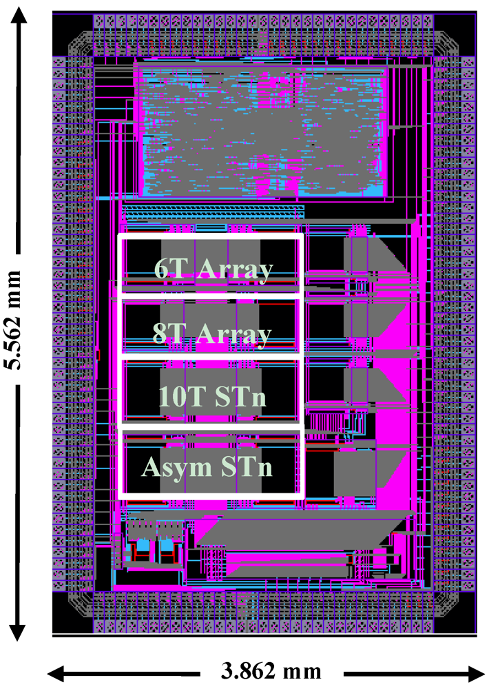
5. Results
To compare bitcell topologies for subthreshold and to test assist features, we implemented a test chip that was fabricated in MITLL 180 nm FDSOI. This technology is specifically optimized for subthreshold operation by using an undoped channel to reduce capacitance and improve V
T control [
18]. In addition, the gate spacer is widened and the source/drain extensions are removed which has only a small impact on I
ON due to low V
DS barrier. These optimizations result in a 50× reduction in energy-delay product compared to bulk silicon. As shown in
Figure 6, the chip contains four SRAM arrays, with each array containing two four-Kb banks. The banks’ dimensions are 128 rows by two 16 bit words. The 6T and 8T cells are sized iso-area; the ST and asymmetric ST bitcells are also iso-area and suffer a 33% area penalty over the 6T and 8T bitcells. In order to easily test the read and write assist methods, peripheral and bitcell array voltages are controlled by separate supplies. The output pads used level converters to convert from sub-threshold to super-threshold in order to ensure that the data could be read by the Logic Analyzer. Because the main objective was reducing V
MIN, the chip was tested at 20 kHz to ensure that timing errors would not occur.
Figure 6.
Layout of the 180 nm test chip.
Figure 6.
Layout of the 180 nm test chip.
The test setup used a combination of Labview to control Keithley 2400 Source Meters and a Tektronix TLA7012 Logic Analyzer to handle the input and output signals. To determine the minimum data retention voltage (DRV), the memory is written with a known value, the voltage is dropped below nominal, then raised back to nominal and the data is read back out. The DRV is defined as the minimum voltage that the memory will retain the data. The second metric, write VMIN is determined in a similar way. First a known value is written at nominal VDD, then the voltage is dropped and the opposite value is written. Next the voltage is raised back to nominal and read back out. To determine read VMIN, a known value is written at nominal VDD, then the voltage is dropped and the data is read back out. Each of the tests described above is an iterative process, with the voltage dropping lower at each step until it is close to ground.
Because the test chip was fabricated during the first run of a new technology (MITLL 180 nm FDSOI), the yield was not ideal. We found full columns to be non-functional as well as a relatively high number of random bit failures. However, even with the non-ideal yield we were able to obtain some interesting results. The first result was that the SRAM proved to be write limited, meaning that the write VMIN exceeded the read VMIN. The best case write VMIN at 80% yield was 620 mV, and the best case read VMIN was 440 mV at 80% yield. This number was chosen because the yield of some of the arrays even at nominal voltage was below 90%. Therefore in order to capture the trends of the various assist methods, we chose to use a yield value of 80% in order to negate the effect of these outliers. The 8T bitcell offered the lowest read VMIN which is surprisingly only 10% lower than the other three bitcells. This is interesting because in simulation, the RSNM of the asymmetric ST and 10T ST bitcells was much higher than the 6T bitcell. What we observed was that there seems to be a discrepancy between the spice models and silicon data. This is most likely due to the technology being relatively immature during its first fabrication run. As a result, it was difficult to compare bitcell topologies, which ended up producing very similar results in silicon. The cause of these discrepancies is not yet fully understood, and more research will be necessary to identify the source of error.
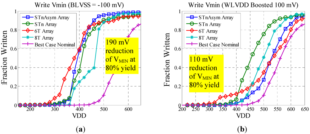
Figure 7.
(a) effect of BL VSS reduction on write VMIN; (b) effect of WL VDD boosting on write VMIN; best case nominal refers to the bitcell with the lowest write VMIN without the use of assist methods.
Figure 7.
(a) effect of BL VSS reduction on write VMIN; (b) effect of WL VDD boosting on write VMIN; best case nominal refers to the bitcell with the lowest write VMIN without the use of assist methods.
Table 1.
Percentage reduction in write VMIN relative to write VMIN without assist methods.
Table 1.
Percentage reduction in write VMIN relative to write VMIN without assist methods.
| Bitcell | BLVSS | WLVDD |
|---|
| 6T | 30% | 3% |
| 8T | 23% | 12% |
| 10T ST | 27% | 18% |
| Asym. ST | 30% | 7% |
Although bitcell measurements yielded inconclusive results, we can still evaluate assist features. The results from the different write assist methods are shown in
Figure 7 and
Table 1. Based on these figures, we conclude that BL VSS reduction is the most effect method for reducing write V
MIN. This method outperforms the WL V
DD boost method across each of the bitcells. It is interesting to note that the 6T bitcell and Asymmetric ST bitcell achieve the lowest write V
MIN at 430 mV, a reduction of 190 mV compared to the best case without assist methods.
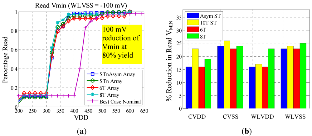
As seen in
Figure 8a, the WL V
SS reduction resulted in a 100 mV reduction in read V
MIN for each of the bitcells. The interesting trend with this plot is that each of the bitcells had almost identical read V
MIN values. This would suggest using a combination of the 6T bitcell and WL V
SS reduction is the most area efficient strategy for reducing read V
MIN. Based on the results from
Figure 8b, reducing WL V
SS and bitcell V
SS consistently improved the read V
MIN for each of the bitcells. This suggests that bitline leakage was a major contributor to reduced read margin. It is also interesting to note that increasing the bitcell V
DD had the greatest impact on the 10T ST bitcell and WL V
DD boosting had the most positive effect on the 8T bitcell. Again, process features in the new technology most likely masked the effects of topological differences in the cells.
Figure 8.
(a) Effect of WL VSS reduction on read VMIN; (b) comparison of read assist methods.
Figure 8.
(a) Effect of WL VSS reduction on read VMIN; (b) comparison of read assist methods.
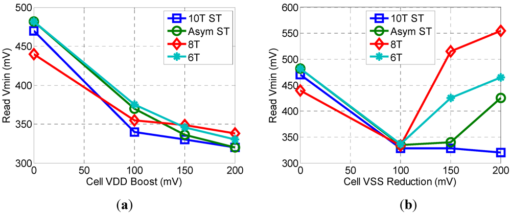
Figure 9.
Effects of boosting the cell VDD (a) and the reducing the cell VSS (b) below 100 mV.
Figure 9.
Effects of boosting the cell VDD (a) and the reducing the cell VSS (b) below 100 mV.
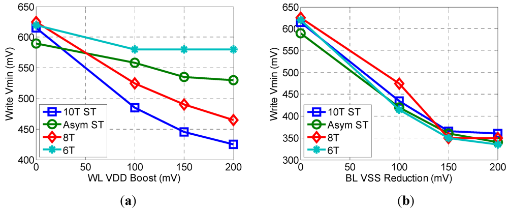
Figure 10.
Effects of increasing the WL VDDBoost (a) and BL VSS Reduction (b) above 100 mV.
Figure 10.
Effects of increasing the WL VDDBoost (a) and BL VSS Reduction (b) above 100 mV.
Figure 9a shows that as the cell V
DD is boosted above 100 mV, the effect it has on reducing read V
MIN degrades. Increasing the cell V
DD from 100 mV to 200 mV results in only a 9% average reduction in read V
MIN.
Figure 9b shows that reducing the cell VSS below −100 mV actually results in an increase in read V
MIN. This is likely due to the forward biasing of the source to bulk junction. Not shown in
Figure 9 is the effect of increasing the WL V
DD and V
SS from 100 to 200 mV, because this increase had no effect on the read V
MIN. This is most likely due to the fact that the measured data retention voltage (DRV) ranged from 300 to 350 mV.
The results in
Figure 10 show the effect of raising the assist voltage above 100 mV and are measured at a yield of 70%. As seen in
Figure 10a, as the WL V
DD is boosted up to 200 mV greater than nominal V
DD, the write V
MIN of the 10T ST and the 8T bitcells improve consistently. However, the 6T bitcell sees no improvement in V
MIN as the WL V
DD is boosted above 100 mV. Reducing the BL V
SS below −100 mV has a significant effect on reducing the write V
MIN. For the 8T bitcell, a reduction from −100 mV to −150 mV results in a 26% reduction in V
MIN. However, further reducing the BL V
SS to −200 mV does not have a significant effect on reducing V
MIN. Based on this data we conclude that using a combination of the 6T bitcell and negative BL V
SS is the most area efficient strategy for reducing write V
MIN.


