Article

Class E ZVS Resonant Inverter with CLC Filter and PLL-Based Resonant Frequency Tracking for Ultrasonic Piezoelectric Transducer

by
Apinan Aurasopon
1,
Boontan Sriboonrueng
2,*,
Jirapong Jittakort
2 and
Saichol Chudjuarjeen
3
1
Faculty of Engineering, Mahasarakham University, Mahasakham 44150, Thailand
2
Department of Electrical Engineering, Faculty of Technical Education, Rajamangala University of Technology Thanyaburi, Pathum Thani 12120, Thailand
3
Department of Electrical and Telecommunication, Rajamangala University of Technology Krungthep, Bangkok 10120, Thailand
*
Author to whom correspondence should be addressed.
J. Low Power Electron. Appl. 2025, 15(3), 54; https://doi.org/10.3390/jlpea15030054
Submission received: 15 July 2025 / Revised: 4 September 2025 / Accepted: 16 September 2025 / Published: 22 September 2025

Abstract

This paper presents a Class E zero-voltage soft-switching (ZVS) resonant inverter integrated with a CLC filter and a digital resonant frequency tracking technique for driving a piezoelectric ceramic transducer (PZT) in ultrasonic cleaning applications. A digital signal processor (DSP) is used to dynamically monitor and adjust the operating frequency in response to slight variations in the cleaning load, employing a phase-locked loop (PLL) control scheme. The proposed method ensures that the inverter maintains ZVS operation across a frequency range from 30.0 kHz to 34.0 kHz, thereby improving energy efficiency and reducing switching losses. The system is capable of delivering a stable power output of 100 W. Both the simulation and experimental results validate the effectiveness of the proposed technique, demonstrating improved performance under varying load conditions. The combination of CLC filtering and frequency tracking offers a compact and robust solution suitable for ultrasonic cleaner systems and similar resonant-load applications.

1. Introduction

Ultrasonic cleaning is a well-established technology widely used for removing contaminants from the surfaces of objects, particularly in areas that are difficult to access using conventional methods [1,2,3,4,5,6,7]. A piezoelectric ceramic transducer (PZT) is typically used to convert electrical energy into high-frequency ultrasonic waves, generally above 20 kHz, which generates microscopic cavitation bubbles in a liquid medium to dislodge and eliminate dirt and particles from the target surface [3,6,8,9,10,11,12]. This technique enables efficient and thorough cleaning without requiring many harmful chemicals, making it suitable for delicate or intricate items.
Ultrasonic cleaners are employed across various industries, including medical device sterilization, electronic component cleaning, and the maintenance of optical instruments, like camera lenses, microscopes, and telescope parts. To efficiently drive the PZTs in such systems, resonant inverters are widely developed and optimized. Several inverter topologies, such as full- and half-bridge and Class D and E resonant inverters, have been investigated for ultrasonic applications [6,13,14,15,16,17]. Among them, the Class E resonant inverter is especially attractive due to its high efficiency, reduced electromagnetic interference (EMI), low conduction losses, minimal component count, and its ability to maintain ZVS under ideal conditions [13,18,19,20,21,22].
However, maintaining ZVS becomes challenging when the system is subjected to variations in load or changes in the resonant frequency of the PZT. For instance, the predictive current control approach proposed in [4] for a Class E inverter fails to compensate for such frequency shifts, leading to operation outside the ZVS condition and a drop in overall efficiency. This issue is compounded by the narrow resonant and anti-resonant frequency range of the PZT, which limits the effective control margin of conventional inverters. To address this limitation, prior work has proposed extending the operating range of the inverter using a series inductive filter in a Class D topology [6]. More recently, CLC filters have been employed in power electronics to suppress EMI, enhance power quality, and reduce switching losses [11,23,24,25,26]. In addition, digital control techniques such as PLL algorithms have proven effective for dynamically tracking resonant frequency variations in real time [27,28,29,30].
This paper proposes an enhanced Class E ZVS resonant inverter architecture that incorporates a CLC filter and a PLL-based resonant frequency tracking algorithm implemented on a digital signal processor (DSP). The proposed system is designed to ensure continuous ZVS operation even under dynamic load conditions, thereby improving the reliability and efficiency of ultrasonic cleaners. The remainder of this paper is organized as follows: Section 2 describes the overall system architecture and circuit topology. Section 3 provides a detailed analysis of the resonant circuit. Section 4 presents the hardware implementation along with the simulation and experimental results. Finally, Section 5 concludes the findings and discusses the advantages of the proposed approach.

2. Proposed System

Figure 1 illustrates the overall architecture of the proposed ultrasonic cleaning system. It is composed of three main stages: a full-bridge rectifier, a Class E ZVS resonant inverter, and an ultrasonic cleaning tank equipped with a PZT. The input AC voltage vi, typically of the mains at a frequency of 50 Hz, is first converted into a DC voltage Vdc by the full-bridge rectifier. To reduce the ripple in the DC supply and maintain a steady current, a high-value choke inductor L 1 is placed after the rectifier. This ensures smooth energy delivery to the inverter stage. The DC voltage is then fed into the Class E ZVS resonant inverter, which converts it into a high-frequency AC signal with a switching frequency f s in the range of 25–35 kHz. This frequency range is carefully chosen to match the resonant characteristics of the PZT, thereby maximizing the efficiency of ultrasonic energy generation. The inverter drives the PZT mounted beneath or within a water tank. When excited at its resonant frequency, the PZT produces ultrasonic vibrations that propagate through the liquid medium and generate cavitation bubbles. These bubbles collapse near the surface of the immersed workpiece, effectively dislodging contaminants in a non-invasive manner.
The proposed configuration leverages the advantages of Class E ZVS switching—such as reduced switching losses, lower EMI, and high efficiency—while maintaining stable operation under varying load conditions. To achieve this, a PLL algorithm implemented on a DSP continuously tracks the resonant frequency of the PZT and adjusts the switching frequency accordingly. This system is particularly suitable for high-performance ultrasonic cleaning applications where both energy efficiency and cleaning effectiveness are critical.
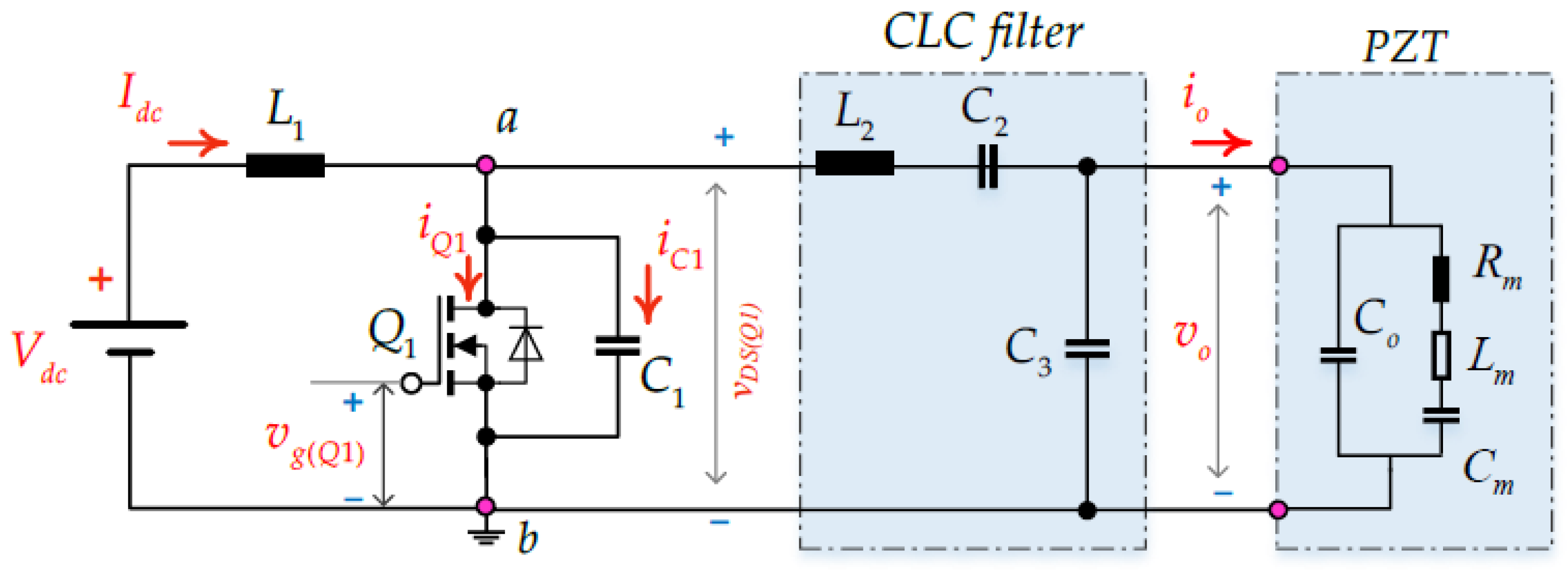
Figure 2 presents the detailed schematic of the proposed Class E ZVS resonant inverter system integrated with a CLC filter, specifically designed for driving a PZT in ultrasonic cleaning applications. The system is powered by a DC supply voltage V d c , which is typically obtained from a full-bridge rectifier, as shown earlier in Figure 1. A choke inductor L 1 is connected in series to suppress voltage ripple and maintain a relatively constant current I d c flowing into the inverter stage. The inverter stage consists of a single MOSFET switch Q 1 operating under ZVS conditions. A parallel capacitor C 1 is connected across the MOSFET to facilitate soft switching and reduce voltage stress during turn-off transitions. When Q 1 is switched ON and OFF at a high frequency (typically 25–35 kHz), it generates a quasi-sinusoidal current waveform i o that flows into the resonant-load network. The CLC filter—composed of a series inductor L 2 , a series capacitor C 2 , and another shunt capacitor C 3 —functions as a resonant matching network between the inverter and the PZT. This network not only improves power transfer efficiency, but also shapes the output waveform and filters out unwanted harmonics, resulting in a smoother output voltage v o across the load.
On the output side, the PZT is modeled as an equivalent circuit containing a motional branch with inductance L m , resistance R m , and capacitance C m , representing the mechanical vibration dynamics of the transducer. A parallel capacitor C o accounts for the static capacitance of the PZT structure. The interaction of these components determines the resonant or anti-resonant behavior of the transducer. By precisely adjusting the switching frequency of Q 1 to match the PZT’s resonant frequency using a DSP-controlled PLL, the system ensures maximum energy transfer and maintains the ZVS condition under varying load scenarios. This circuit configuration combines the simplicity and high efficiency of Class E operation with the filtering and impedance matching benefits of the CLC network, making it well-suited for compact and energy-efficient ultrasonic cleaning systems.
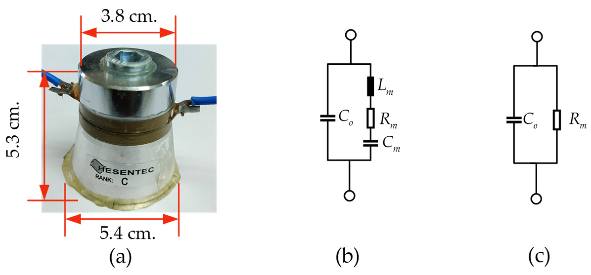
Figure 3 presents physical and simplified electrical models of the piezoelectric ceramic transducer (PZT) used in the proposed system. Figure 3a shows the actual structure of the PZT used in the experimental prototype. The device has a cylindrical form factor, with a diameter of 5.4 cm and a height of 5.3 cm. It is designed to convert high-frequency electrical signals into ultrasonic vibrations for cleaning applications. Figure 3b illustrates the detailed equivalent circuit of the PZT, which includes a motional branch consisting of the elements L m , R m , and C m . These elements represent the mechanical characteristics of the transducer: L m models inertia (mass), R m accounts for energy dissipation (mechanical loss), and C m corresponds to elasticity (compliance). This motional branch is connected in parallel with static capacitance C o , representing the dielectric property of the transducer material. Figure 3c shows a simplified steady-state equivalent model. Under resonance, motional impedance becomes minimal, allowing for the PZT to be approximated as a parallel combination of C o and R m . This simplification is useful for impedance matching and circuit analysis when designing the resonant inverter and the CLC filter.
The design of the inverter to control the PZT load must be based on the impedance and phase graph of the piezoceramic transducer (PZT), which was previously presented in reference [31], as shown in Figure 2. Two frequencies occur: resonant ( f r ) and anti-resonant frequencies ( f a ). When the switching frequency ( f s ) of the inverter operates in the range of f r < f s < f a , the PZT load is inductive, causing a lagging phase. In this case, the inverter operates under ZVS conditions. However, if the frequency is f s < f r or f s > f a , the PZT load is capacitive, causing a leading phase. In this case, the inverter operates under non-ZVS conditions, which can damage the switches. The measured frequencies of the PZT load are f r = 28 kHz and f a = 36 kHz. Therefore, to ensure the inverter operates under ZVS conditions, the frequency f s should be in the range from 28 kHz to 36 kHz.
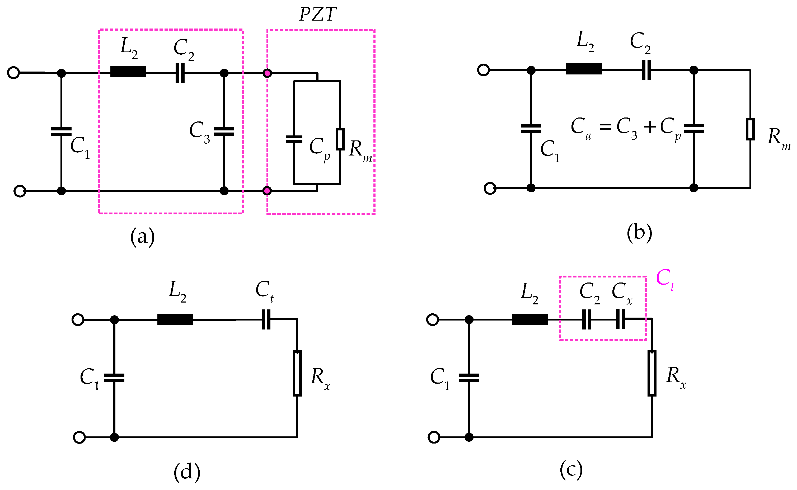
Figure 4 presents the step-by-step equivalent circuit transformation of the CLC filter combined with the PZT load, which is necessary for accurate impedance modeling and resonant frequency analysis of the system. Figure 4a shows the original configuration, where the CLC filter—comprising L 2 , C 2 , and C 3 —is connected to the PZT load modeled by a parallel combination of static capacitance C o and motional resistance R m . For analytical purposes, capacitance C o is combined with C 3 , as shown in the next stage. Figure 4b simplifies the parallel capacitors C 3 and C o into a single equivalent capacitance, denoted as C a , using the following equation:
C a = C 3 + C o .
Figure 4c converts the parallel combination of C a and R m into an equivalent series RC circuit defined by the parameters R x and C x , given by the following equation:
R x = R m 1 + ω 2 R m 2 C a 2
C x = 1 + ω 2 R m 2 C a 2 ω 2 R m 2 C a .
where ω = 2πf is the angular frequency of operation.
Figure 4d further reduces the combination of series capacitors C 2 and C x into a single effective capacitance C t , using the following standard series formula:
C t = C 2 C x C 2 + C x .
All the variables represented in Figure 4 are listed in Appendix A.

3. Circuit Analysis

  • The analysis of the proposed Class E ZVS resonant inverter is based on the following assumptions:
  • The power MOSFETs operate as ideal switches.
  • The quality factor Q L of the series resonant load is sufficiently high, ensuring a nearly sinusoidal output current i o .
  • The input current I d c is considered constant due to the large choke inductor L 1 .
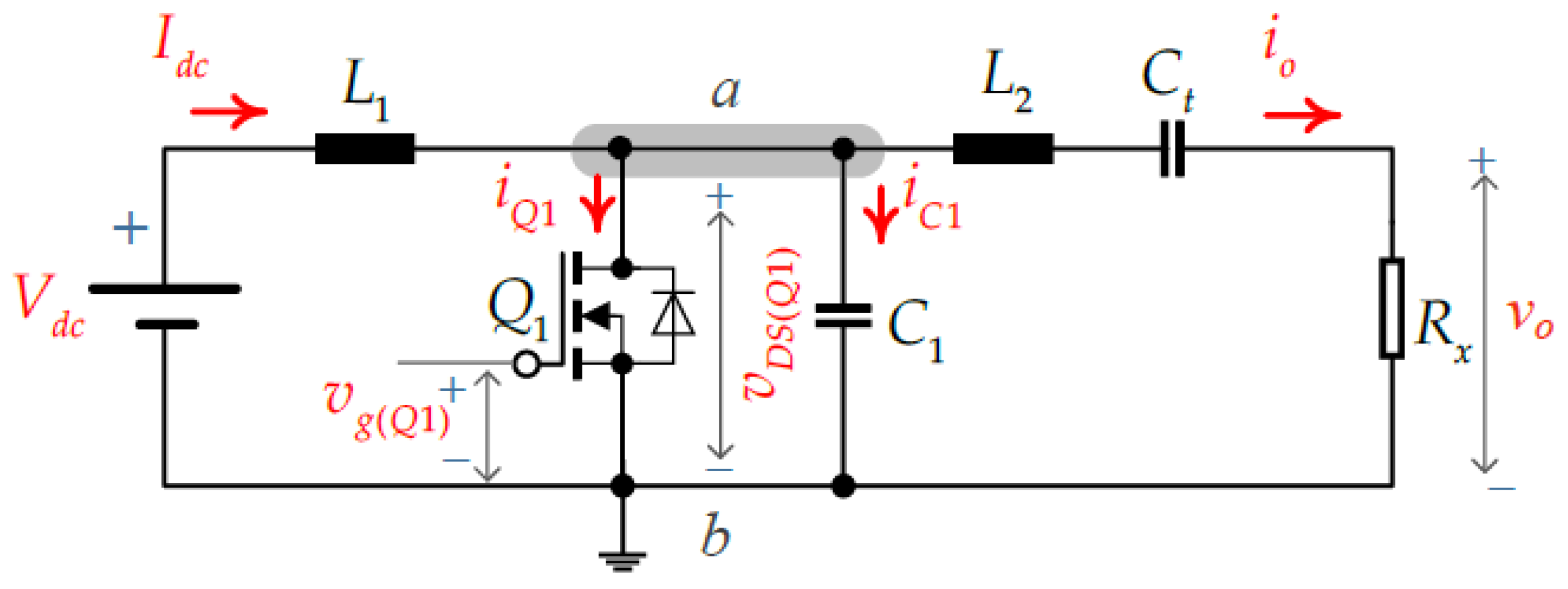
Figure 5 illustrates the equivalent circuit of the Class E ZVS resonant inverter. High-frequency switching is performed by the power switch Q 1 , with its gate signal v g ( Q 1 ) . A shunt capacitor C 1 enables ZVS by shaping the voltage waveform across the MOSFET. The series LC branch consisting of L 2 and C t , followed by the resistive component R x , represents the load network connected to the ultrasonic transducer.
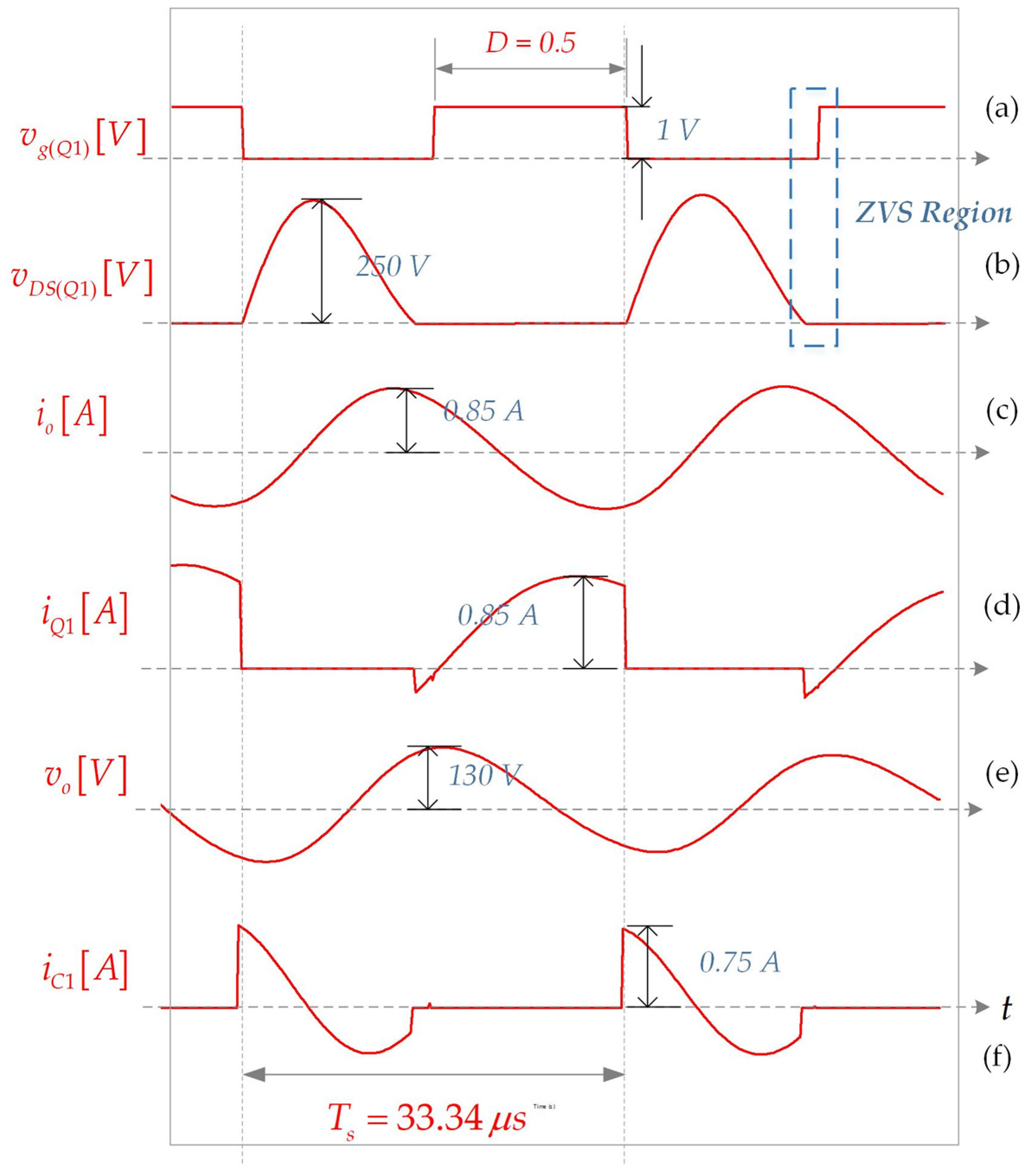
Figure 6 shows the key voltage and current waveforms within one switching cycle T s . The waveforms include:
  • v g ( Q 1 ) : gate drive signal of the MOSFET.
  • v D S ( Q 1 ) : drain–source voltage of Q 1 .
  • i Q 1 : current through switch Q 1 .
  • i C 1 : current through the shunt capacitor C 1 .
  • i o : output current delivered to the load.
  • v o : voltage across the load.
The output current i o of the resonant circuit is assumed to follow a sinusoidal form:
i o = I o max sin ω t + θ
where I o max is the peak output current, ω = 2 π f s is the angular frequency, and θ is the phase angle. The switching behavior of Q 1 is characterized as follows:
  • Q 1 is turned ON when the capacitor current i C 1 becomes zero at ω t = 0 , ensuring ZVS.
  • During the ON interval 0 < ω t < D T s , the current through Q 1 , i Q 1 , is
    i Q 1 = I d c I o max sin ω t + θ , f o r 0 < ω t < D T s 0 , f o r D T s < ω t < T s .
During the OFF interval D T s < ω t < T s , the current flows through capacitor C 1 is
i C 1 = 0 , f o r 0 < ω t < D T s , I d c I o max sin ω t + θ , f o r D T s < ω t < T s .
Applying Kirchhoff’s Current Law at node a in Figure 5, the total output current is
i o = I d c i C 1 + i Q 1
which can be rearranged to
i C 1 + i Q 1 = I d c i o
Substituting Equation (5) into Equation (9) and analyzing at the boundary where i C 1 = 0 , the peak output current becomes
I o [ max ] = I d c T s 1 D cos D T s + θ cos θ .
The output power of the resonant circuit is given by
P o = R x I o [ max ] 2 2 .
Finally, substituting Equation (10) into Equation (11), the output power of the Class E ZVS resonant inverter becomes
P o = R x 2 I d c T s 1 D cos D T s + θ cos θ 2 .
This analytical model enables the evaluation of inverter performance, such as current stress, switching conditions, and output power, under varying duty cycles and frequency shifts.
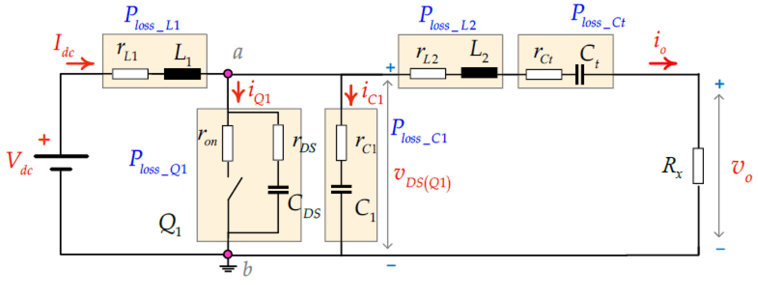
The analysis of power losses of the proposed inverter for the ultrasonic cleaning application, based on the Class E ZVS resonant inverter shown in Figure 5, can be represented by the equivalent circuit of a Class E resonant inverter with parasitic resistances, as shown in Figure 7. In the operation of a Class E ZVS resonant inverter, the parasitic resistances of circuit components play a decisive role in determining overall efficiency. In particular, the power switch exhibits intrinsic on-resistance, which leads to conduction losses. These losses not only degrade the efficiency of the system but also cause thermal accumulation and may compromise the ZVS condition. Moreover, the parasitic resistances of the inductor and capacitor, represented by their equivalent series resistances (ESRs), contribute significantly to power dissipation. Since large resonant currents flow through these passive elements, the ESRs of both the inductor and the capacitors become the dominant factor responsible for the noticeable reduction in inverter efficiency.
The power losses of a Class E ZVS resonant inverter for the ultrasonic cleaning application consist of three components: (1) power loss due to the parasitic resistance of the power MOSFET, (2) switching loss during the turn-on of the power MOSFET, and (3) power losses in the inductor and the capacitor filter.
(1)
The power losses due to the parasitic resistance of the power MOSFET Q 1 occur in two stages: the power loss when the power MOSFET Q 1 conducts current depends on the MOSFET on-resistance, r o n , and the power loss due to the internal resistance (ESR or equivalent series resistance) of the capacitance between the drain and source in the MOSFET Q 1 , r D S . The power loss equations for both cases can be expressed as follows:
P l o s s _ r o n = 1 T s 0 T s r o n i Q 1 2 d ω t = r o n i Q 1 _ r m s 2
P l o s s _ r D S = 1 T s 0 T s r D S i Q 1 2 d ω t = r D S i Q 1 _ r m s 2 .
(2)
The switching loss is caused by energy stored in the parasitic capacitance during the transition of the switch from the off state to the on state. The total loss is calculated as the average of the energy stored during the switching cycle, which affects the circuit’s efficiency, especially at high switching frequencies. This loss can be reduced by improving the control of the switching process. Therefore, the power loss during the turn-on of the power MOSFET Q 1 is
P l o s s _ S W = W t u r n o n T s
where the energy stored during the switching cycle is
W t u r n o n = 0 v D S _ o n C 1 v D S d ω t = C 1 V D S _ r m s .
(3)
The power losses caused by the parasitic resistances of the inductor and capacitors include the power loss of inductor L 1 , P l o s s _ L 1 ; power loss of capacitor C 1 , P l o s s _ C 1 ; power loss of inductor L 2 , P l o s s _ L 2 ; and power loss of capacitor C t , P l o s s _ C t . Therefore, the power losses due to the parasitic resistances of the inductor and capacitors are expressed by the following equations:
P l o s s _ L 1 = r L 1 I d c 2
where r L 1 is the parasitic resistance of the inductor L 1 .
P l o s s _ C 1 = 1 T s 0 T s r C 1 i C 1 2 d ω t = r C 1 I C 1 _ r m s 2
where r C 1 is the parasitic resistance of the capacitor C 1 .
P l o s s _ L C = 1 T s 0 T s r L 2 + r C t i o 2 d ω t = r L 2 + r C t I o _ r m s 2
where r L 2 is the parasitic resistance of the inductor L 2 , and r C t is the parasitic resistance of the capacitor C t .
Therefore, the total power losses of the Class E resonant inverter can be calculated as follows:
P t _ l o s s = P l o s s _ r o n + P l o s s _ r D S + P l o s s _ S W + P l o s s _ L 1 + P l o s s _ C 1 + P l o s s _ L C .
Consequently, the efficiency of the Class E resonant inverter can be determined as follows:
η = P o P o + P t _ l o s s .
The system efficiency calculation is presented in Appendix A.

4. Implementation and Results

4.1. Implementation

Figure 8 illustrates the control architecture of the proposed ultrasonic cleaning system, in which the Class E ZVS resonant inverter with a CLC filter drives the PZT-based ultrasonic cleaner. A TMS320F28335 digital signal processor (DSP) is used as the main controller and is manufactured by Texas Instruments, which is based in Dallas, Texas, USA. This device operates at a clock speed of 150 MHz with a 32-bit fixed-point architecture and supports a 10 kHz sampling rate, providing real-time control over the inverter’s switching operation.
To maintain optimal ZVS conditions under varying load conditions—such as changes in water volume and cleaning load—the system employs a PLL algorithm. The PLL block consists of a phase detector, a PI controller, a low-pass filter (LPF), and a voltage-controlled oscillator (VCO). Together, these modules dynamically track the resonant frequency of the PZT and adjust the inverter switching frequency accordingly.
The zero-crossing detector circuit shown in Figure 9 is used to monitor the output current i o and detect its phase. This analog signal is conditioned using the TLV7011 comparator (U1) from Texas Instruments, which is based in Dallas, Texas, USA. The circuit detects the zero-crossing point of the sinusoidal i o waveform and converts it into a digital pulse signal, which is sent to the DSP via its analog input pin A1.
Figure 9 shows the zero-crossing detector circuit, applying an op-amp comparator (TLV7011) to detect the output current of the Class E resonant inverter, characterized by a sinusoidal waveform or AC signal from a current sensor of LAM (LA 100-P) from California, USA, to execute zero-crossing and level-shift the voltage to retain only the positive half. From the circuit, R 1 (100 kΩ) and R 2 (4.7 kΩ) are used as a voltage divider to attenuate the AC signal before it is sent to the non-inverting input of the comparator. D 1 represents a diode that keeps the non-inverting input of the comparator from falling below the minimum allowed value dictated by the negative input common-mode voltage limit. The output of the zero-crossing detection circuit, V r e f _ A , is a pulse signal that switches between 0 V and 3.3 V at the frequency f s . This signal is then sent to the A 1 pin of the TMS320F28335 DSP.
Figure 10 presents the opto-isolation circuit used to safely transmit gate control signals to the power stage. The opto-isolator TLP250 (U2) from Toshiba (Electronic Source Company, Bangkok, Thailand) is used to provide electrical isolation between the low-voltage control and high-voltage switching sides. The circuit is powered by a +15 V supply and includes appropriate current-limiting resistors for reliable operation.
To characterize the PZT used in the system, an LCR meter (HIOKI 3532-50) was employed form Electronic Source Company, Bangkok, Thailand. The key parameters of the transducer, including the mechanical and electrical components, are listed in Table 1. These values were used in both the simulation and the experimental analysis.
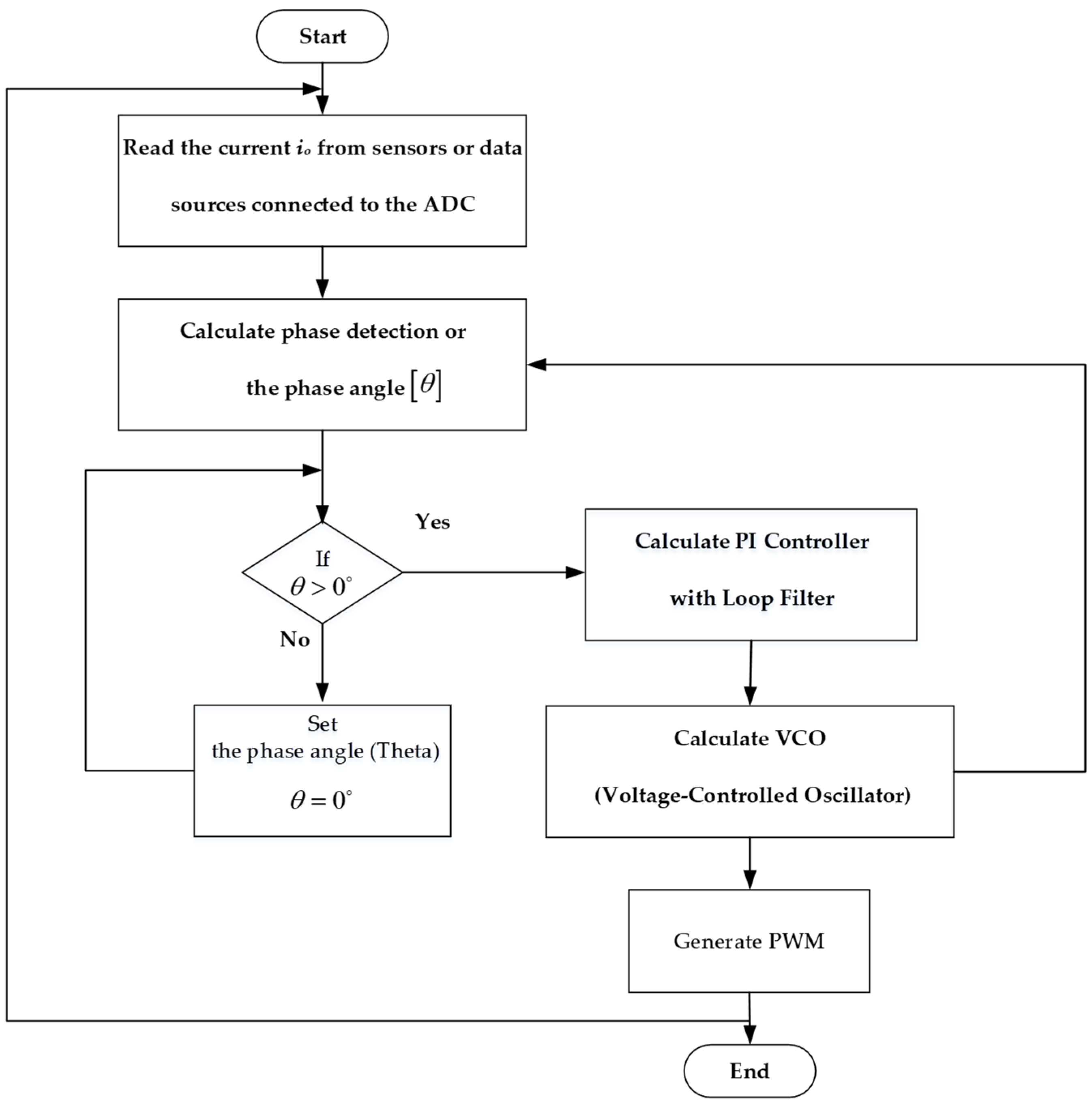
Figure 11 shows a process diagram of the system implemented to maintain the frequency variations for the load in ultrasonic cleaning. The procedure started by acquiring the output current i o data from the sensor connected to the ADC (analog-to-digital converter) for subsequent processing. Subsequently, the system computes the phase detection or phase angle from the acquired data. The system subsequently verifies if the phase angle (θ) exceeds 0. If the phase angle is not zero, the system adjusts it to zero and reprocesses the data. When the phase angle is zero, the system calculates the PI controller using a loop filter for enhanced control precision. Afterwards, the system computes the VCO (voltage-controlled oscillator), which controls frequency regulation. Finally, the system produces a PWM (Pulse Width Modulation) signal to regulate its functioning, thereby concluding the process.
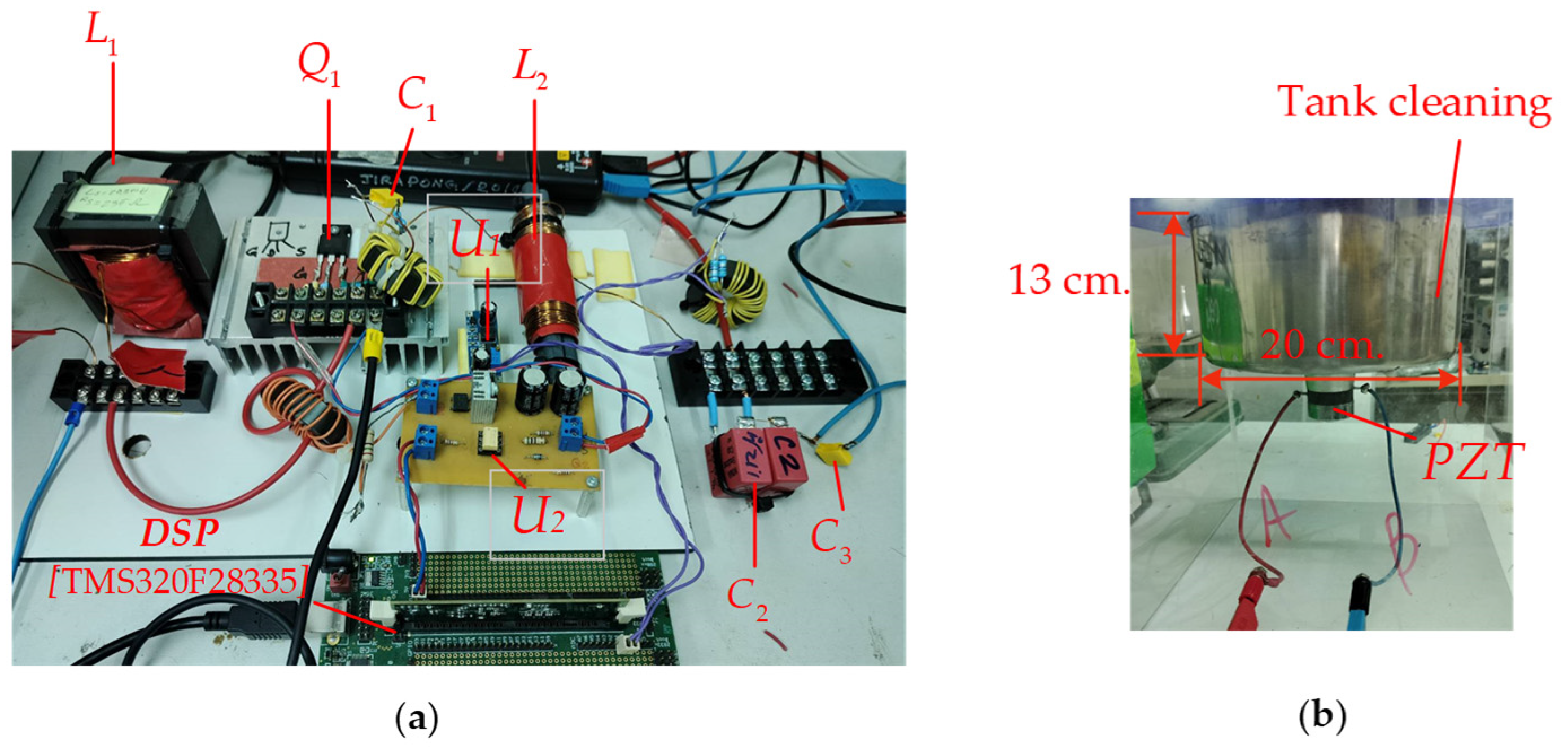
To validate the operational principles and theoretical analysis of the proposed Class E ZVS resonant inverter system, a laboratory prototype was developed, as shown in Figure 12. Figure 12a depicts the physical implementation of the inverter circuit. The system includes the power switch Q 1 , implemented using an IRFP460 MOSFET from Electronic Source Company, Bangkok, Thailand, along with the resonant elements and the CLC filter components C 1 , C 2 , C 3 , and L 2 . The circuit is controlled by a TMS320F28335 DSP, with the driver and isolation circuitry (including U1 and U2) positioned on a compact test board. Figure 12b shows the experimental ultrasonic cleaning tank, where a PZT is mounted at the bottom of a stainless steel container (dimensions: 20 cm × 13 cm). The transducer is driven at resonance to generate ultrasonic waves for cleaning applications.
This setup was tested with various cleaning targets, including printed circuit boards, jewelry, stainless steel parts, plastic components, and electrical contacts, demonstrating the practical effectiveness and versatility of the proposed system in real-world ultrasonic cleaning tasks.

4.2. Results

To verify the performance of the proposed Class E ZVS resonant inverter with CLC filtering, both the simulation and experimental results were analyzed under varying load conditions. Figure 13 presents the simulated waveforms at a switching frequency f s = 30 kHz and a duty cycle D = 0.5, demonstrating proper ZVS operation. The gate–source voltage v g Q 1 is shown in Figure 13a, while the corresponding drain–source voltage v D S Q 1 , peaking at 250 V, is depicted in Figure 13b. The output current i o and the switch current i Q 1 both reach a maximum of 0.85 A, as shown in Figure 13c,d, respectively. The output voltage v o , across the load, reaches 130 V peak as illustrated in Figure 13e. The shunt capacitor current i C 1 , shown in Figure 13f, peaks at 0.75 A. Under these conditions, the simulated output power P o is approximately 90 W.
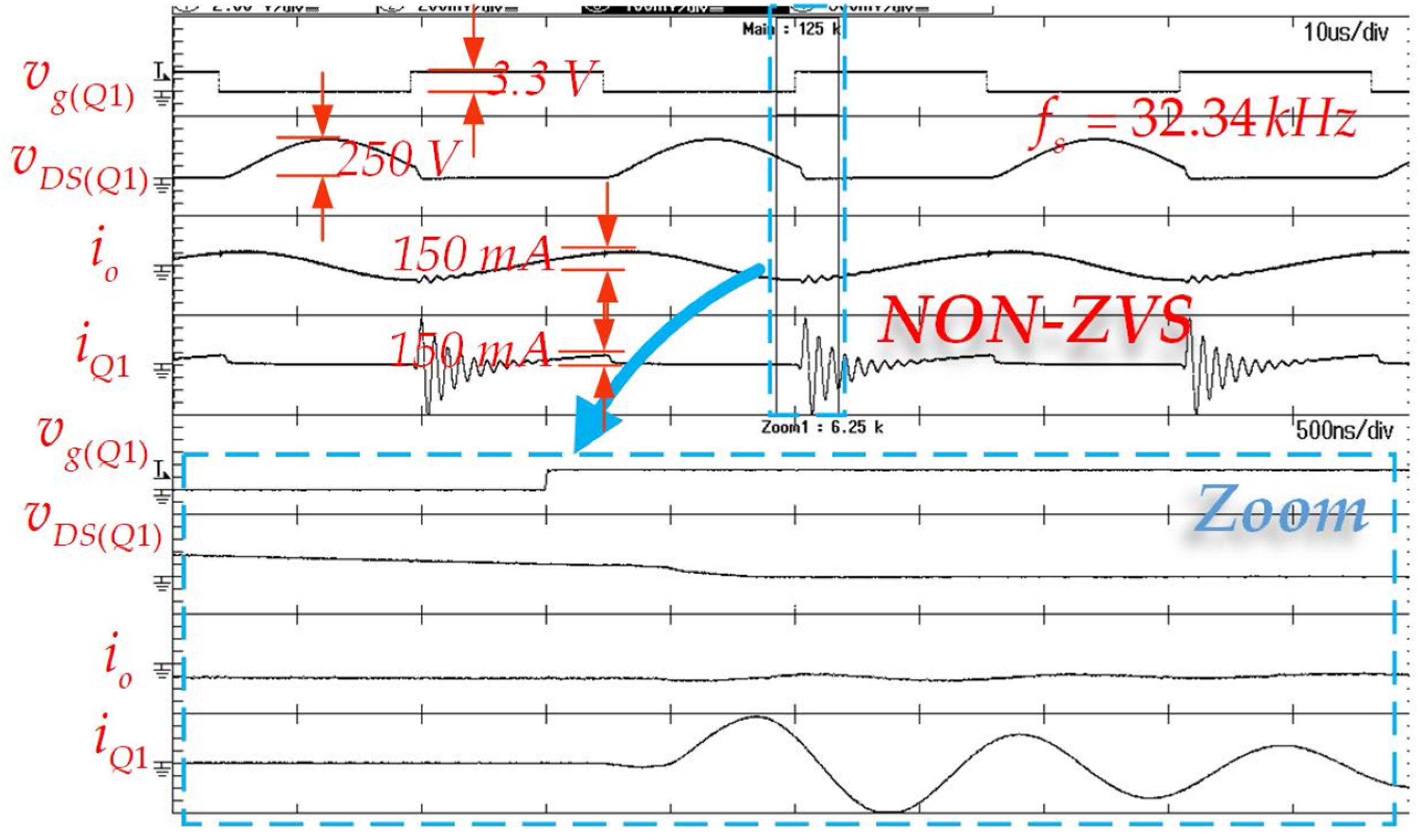
Figure 14 illustrates the experimental waveforms of the inverter operating at f s = 32.34 kHz and a duty cycle D = 0.5, without employing the resonant frequency tracking control. In this case, as the liquid level in the tank decreases, the resonant frequency of the PZT increases. Since the inverter is not tracking this shift, it begins to operate under a non-ZVS condition, which is clearly visible in the zoomed region of the waveform. The observed oscillations in the current i Q 1 lead to increased switching losses and reduced efficiency.
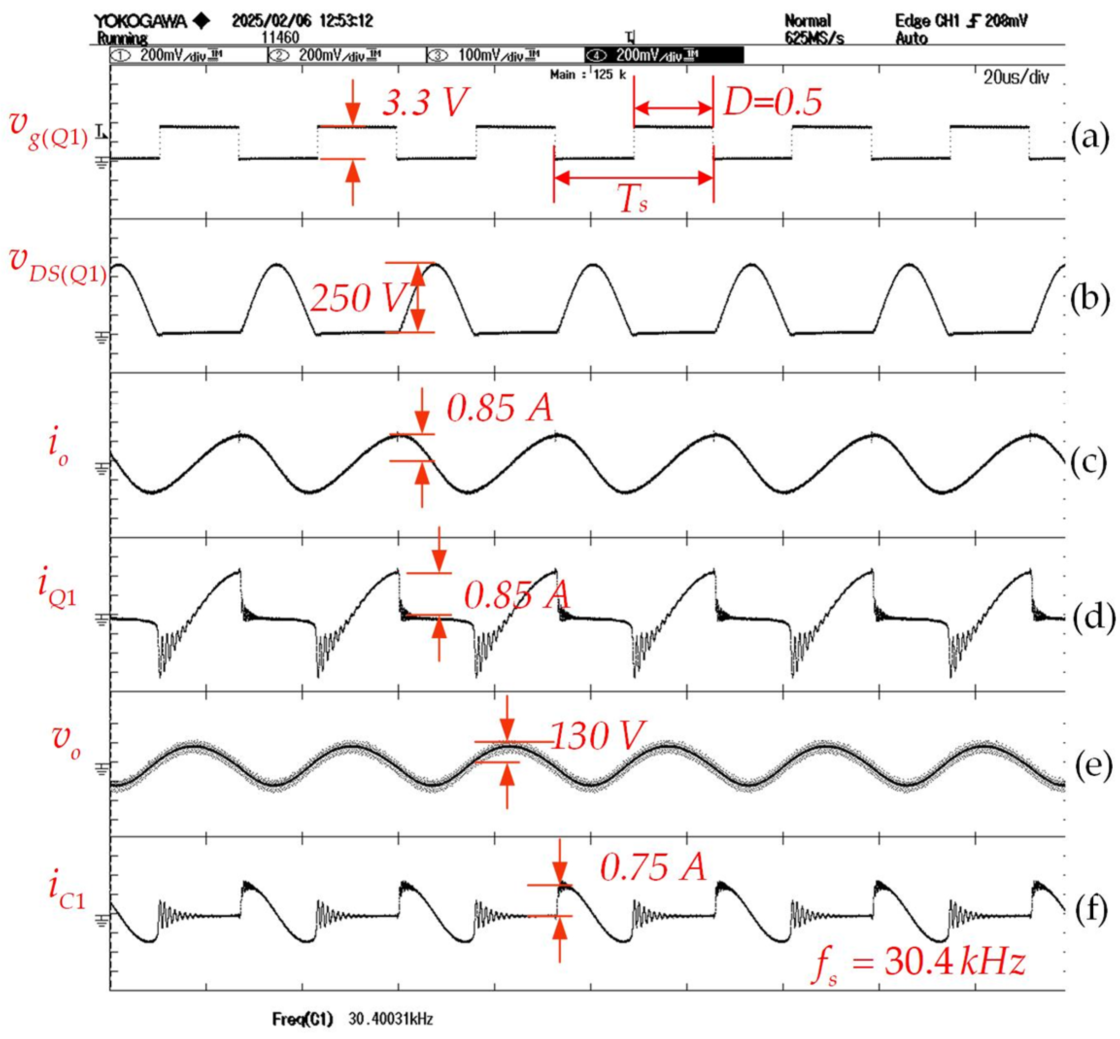
To address this, Figure 15 presents the experimental results with the PLL-based resonant frequency tracking enabled, operating at a frequency f s = 30.4 kHz. Figure 15a shows the 3.3 V gate–source voltage v g Q 1 , while Figure 15b displays the output voltage v o , which peaks at 250 V with an RMS value of 176 V. The output current i o , shown in Figure 15c, reaches a peak of 0.85 A with an RMS value of 0.601 A. The switch current i Q 1 also peaks at 0.85 A, as shown in Figure 15d, and the shunt capacitor current i C 1 peaks at 0.75 A, as shown in Figure 15f. The measured output power in this case is approximately 94.5 W, and the liquid solvent volume in the tank was maintained at 3 L.
These results confirm that the proposed system, when combined with PLL-based resonant frequency tracking, can maintain ZVS operation and deliver stable output power despite variations in the load conditions, thereby improving overall efficiency and system reliability.
The experimental results of the Class E ZVS resonant inverter operating under PLL-based frequency tracking at a switching frequency f s = 32.4 kHz are shown in Figure 16. These results correspond to conditions with a dynamically altered load, where the inverter successfully maintains ZVS operation. The gate–source voltage v g ( Q 1 ) , as shown in Figure 16a, with a duty cycle D = 0.5, reaches a peak of 3.3 V. The drain–source voltage v D S ( Q 1 ) peaks at 250 V, as shown in Figure 16b, confirming proper switching. The output current io, as shown in Figure 16c, and the current i Q 1 , as shown in Figure 16d, both reach a maximum value of 0.85 A.
The oscillatory behavior of i Q 1 , as shown in Figure 16d when the diode conducts, is caused by the excitation of the parasitic L–C network, the reverse recovery charge ( Q r r ), and the large dv/dt at commutation. Such ringing is typical of high-frequency converters; careful layout and appropriate damping networks can suppress it so that has a negligible impact on performance and EMI.
At a liquid solvent volume of 2 L, the system delivers a measured output power value P o of approximately 93.25 W. These results validate the effectiveness of the proposed control strategy in maintaining ZVS and stable power delivery under varying load conditions.
Figure 17 presents the experimental results of the Class E ZVS resonant inverter operating with PLL-based frequency tracking at a switching frequency f s of 32.98 kHz under light-load conditions. These results demonstrate the inverter’s ability to maintain ZVS operation despite dynamic load variations. With a duty cycle D of 0.2, the gate–source voltage v q Q 1 reaches a peak of 3.3 V, while the drain–source voltage v D S Q 1 peaks at 100 V, confirming proper switching performance. The output current i o reaches a maximum of 0.38 A. Under a liquid solvent volume of 1 L, the system delivers an output power P o of approximately 40.5 W. These findings validate the effectiveness of the proposed control strategy in sustaining ZVS operation and ensuring stable power delivery under fluctuating load conditions. The zoom area for the time per division on the horizontal axis, set at 1 µs as shown in Figure 17, can maintain the ZVS region, while the water level in the ultrasonic cleaning tank decreases.
Figure 18a shows the power adjustment at 40% of full load, which is approximately 40 W, with the liquid solvent level in the cleaning tank set to 1 L. The power then adjusts according to the water level increase. When the level reaches 3 L, the power reaches full load, which is 94.5 W. To confirm the operation under full load conditions, the experimental results of the v D S Q 1 voltage and i o current are shown in Figure 18b. The experimental results of the v D S Q 1 voltage and i o current under 40% load are also shown in Figure 18c. The results demonstrate that the proposed inverter operates under ZVS conditions and can effectively track frequency f r according to load changes.

5. Conclusions

This study presents an enhanced Class E ZVS resonant inverter integrated with a CLC filter for ultrasonic cleaning applications. The proposed system incorporates a DSP-based gate drive controller, enabling fast and precise control of the switching operation. To ensure optimal performance under varying load conditions, a phase-locked loop (PLL) algorithm is implemented to dynamically track the resonant frequency of the piezoelectric transducer.
Both the simulation and experimental results confirm the effectiveness of the proposed approach in maintaining high efficiency and reliable operation. The key advantages of the system are summarized as follows:
  • The Class E ZVS resonant inverter successfully maintains zero-voltage switching (ZVS) across a range of resonant frequencies and varying load conditions.
  • The CLC filter effectively smooths the output voltage and current waveforms, improving waveform quality and reducing harmonic distortion.
  • The inverter achieves lower switching losses and offers a compact design, making it suitable for space-constrained applications.
In conclusion, the proposed inverter system demonstrates strong potential for use in ultrasonic cleaners and other applications involving resonant loads, where efficiency, adaptability, and compactness are critical.

Author Contributions

Conceptualization, A.A. and B.S.; methodology, A.A.; software, J.J.; validation, A.A., B.S. and J.J.; formal analysis, J.J.; investigation, B.S.; resources, A.A.; data curation, S.C.; writing—original draft preparation, A.A.; writing—review and editing, B.S.; visualization, S.C.; supervision, B.S.; project administration, J.J.; funding acquisition, A.A. All authors have read and agreed to the published version of the manuscript.

Funding

This research project was financially supported by Mahasarakham University.

Data Availability Statement

The original contributions presented in this study are included in the article. Further inquiries can be directed to the corresponding author.

Acknowledgments

I would like to express my deepest gratitude to Mahasarakham University for their generous and trusting support of our project. This assistance not only facilitated the smooth progress of the research, but also inspired the development of valuable future innovations and research.

Conflicts of Interest

The authors declare no conflicts of interest.

Appendix A

The design specifications for the Class E resonant inverter used in the ultrasonic cleaning system are based on the following operating conditions: the voltage V d c is 250 V; the load quality Q L is defined as 10; the switching frequency is set at 30 kHz; and the maximum output power of the PZT is 100 W.
The shunt capacitor C 1 is calculated using
C 1 = 8 π 4 + π 2 ω R x = 8.45 n F .
The combined parallel capacitor C a , derived from the transformation of the PZT equivalent model, is
C a = R m R x 1 ω r 2 R m 2 = 8.7 n F .
From Equation (1), the capacitor C 3 is obtained as
C 3 = C a C o = 6.17 n F .
The series capacitor C t in the resonant tank is calculated using
C t = 1 L 2 . ω 2 = 36.8 n F .
The parasitic resistance of capacitor C t is calculated using
r C t = r C 2 + r C 3 .
The equivalent series capacitor C x , from Equation (3), is
C x = 1 + ω 2 R m 2 C a 2 ω 2 R m 2 C a = 40.3 n F .
Then, using the series capacitor transformation, C 2 is computed as
C 2 = C x C t C x C t = 424 n F .
Using Equation (2), the equivalent resistive component R x is derived as
R x = 8 4 + π 2 V d c 2 P o = 14.42 Ω .
Overall, the L 1 in a Class E resonant inverter tends to be fairly large because its primary role is to act as a near-constant-current source (an RF choke) that preserves the switch voltage and current waveforms required for reliable ZVS. At the chosen switching frequency, the reactance of L 1 must be much greater than the load’s equivalent resistance, which drives a high inductance value. Since the circuit carries high peak and RMS currents, L 1 must store magnetic energy without saturating; this calls for a ferrite core with a sufficient cross-section and air gap, together with a large litz (stranded) wire to limit heating from skin and proximity effects. These requirements increase the physical size and weight of L 1 . A larger L 1 also helps keep ripple from flowing back into the DC bus and improves EMI behavior. If L 1 is too small, current ripple increases, the waveforms deviate, the ZVS window narrows or is lost, switch voltage overshoot grows, efficiency drops, and EMI worsens. Therefore, L 1 must be “large enough” to avoid these issues.
While increasing the switching frequency reduces the required inductance, and thus the size of L 1 , in ultrasonic applications, the output power is regulated by sweeping the drive frequency around the transducer’s resonance. Therefore, L 1 must be sized to maintain RF-choke behavior across the entire control band, particularly at the lowest operating frequency where the inductive reactance, X L is minimal.
As a result, the achievable size reduction is bounded by the control bandwidth, and higher fs also entails increased magnetic core and switching losses, as well as greater EMI, which must be accounted for in the design.
Additionally, when increasing f s , several key trade-offs must be considered:
  • Core loss and AC copper loss in L 1 and the transformer rise with frequency, increasing the thermal burden.
  • Switching loss, dv/dt stress, and EMI all increase, potentially requiring added snubbers/filters.
Thus, the choke inductor L 1 is
L 1 = 2 1 + π 2 4 R x f s = 3.34 m H .
The series inductor L 2 for the CLC filter is
L 2 = Q L R x ω s = 765 μ H .
Table A1. Summary of proposed system parameters.
NameTheorySimulationExperiment
L 1 3.34 mH3.34 mH3.5 mH
L 2 765 μ H 765 μ H 768 μ H
C 1 8.45 nF8.45 nF8.5 nF
C 2 424 nF424 nF450 nF
C 3 6.17 nF6.17 nF6.5 nF
The parasitic resistances of the proposed system parameters, measured using an LCR analyzer (HIOKI3525 form Electronic Source Company, Bangkok, Thailand) at f = 30 kHz, are r L 1 = 2.75 Ω , r L 2 = 1.85 Ω , r o n = 0.27 Ω , r D S = 0.22 Ω , r C 1 = 0.228 Ω , r C 2 = 0.0054 Ω , and r C 3 = 0.05 Ω .
Example of Power Losses Calculation and Efficiency Determination of a Class-E Resonant Inverter at D = 0.5
-
The power loss of Q 1 due to conduction can be determined from Equation (13).
P l o s s _ r o n = r o n i Q 1 _ r m s 2 = 0.27 0.85 / 2 2 = 0.0975 W .
-
The power loss of the MOSFET drain–source capacitance ESR can be calculated using Equation (14).
P l o s s _ r D S = r D S i Q 1 _ r m s 2 = 0.22 0.85 / 2 2 = 0.0792 W .
-
The turn-on loss of the power MOSFET can be calculated using Equation (15).
P l o s s _ S W = W t u r n o n T s = C 1 V D S _ r m s T s = 8.5 n F 250 / 2 30 × 10 6 = 0.05 W
where T s = 1 f s = 1 3 2.4 k H z = 30 × 10 6   s .
-
The power loss of inductor L 1 can be calculated from Equation (16) as follows:
P l o s s _ L 1 = r L 1 I d c 2 = 2.75 1.05 2 = 3.03 W
where the measured current I d c is 1.05 A.
-
The power loss of capacitor C 1 can be calculated from Equation (17) as follows:
P l o s s _ C 1 = r C 1 I C 1 _ r m s 2 = 0.228 0.75 / 2 2 = 0.064 W .
-
Equation (18) provides the calculation of losses arising from the parasitic resistances of inductor L 2 and capacitor C t , as shown below:
P l o s s _ L C = r L 2 + r C t I o _ r m s 2 = 1.65 + 0.0554 0.85 / 2 2 = 1.025 W .
-
Thus, the total power loss of the proposed system can be calculated from Equation (19) as follows:
P t _ l o s s = 0.0975 + 0.0792 + 0.05 + 3.03 + 0.064 + 1.025 = 4.3457 W .
-
Consequently, the efficiency of the Class E resonant inverter can be calculated from Equation (20) as follows:
η = P o P o + P t _ l o s s = 93.25 93.25 + 4.3457 = 95.55 % .

References

  1. Wang, Z.; Saoud, C.; Wangsiricharoen, S.; James, A.W.; Popel, A.S.; Sulam, J. Label cleaning multiple instance learning: Refining coarse annotations on single whole-slide images. IEEE Trans. Med. Imaging 2022, 41, 3952–3968. [Google Scholar] [CrossRef] [PubMed]
  2. Li, Z.; Xu, Q.; Tam, L.M. A survey on techniques and applications of window-cleaning robots. IEEE Access 2021, 9, 111518–111532. [Google Scholar] [CrossRef]
  3. Rymansaib, Z.; Kurt, P.; Zhang, Y.; Roscow, J.I.; Bowen, C.R.; Hunter, A.J. Ultrasonic transducers made from freeze-cast porous piezoceramics. IEEE Trans. Ultrason. Ferroelectr. Freq. Control 2022, 69, 1100–1111. [Google Scholar] [CrossRef]
  4. Niyomthai, S.; Sangswang, A.; Naetiladdanon, S.; Mujjalinvimut, E. A predictive control of class E resonant inverter for ultrasonic cleaners. In Proceedings of the IECON 2017—43rd Annual Conference of the IEEE Industrial Electronics Society, Beijing, China, 29 October–1 November 2017; pp. 6319–6324. [Google Scholar]
  5. Zhang, Z.; Guan, Y.; Zhao, Q.; Wang, F. Early warning on mass imbalance and clean-in-place strategy for rotor of rotating packed bed. IEEE Access 2020, 8, 44503–44510. [Google Scholar] [CrossRef]
  6. Jittakort, J.; Kitcharoenwat, S. Adjusted power of class d-zvs resonant inverter controlled by buck converter for LCLC resonant tank. J. Power Electron. 2023, 23, 1907–1918. [Google Scholar] [CrossRef]
  7. Srathonghuam, K.; Wonganu, B.; Busayaporn, W.; Thongsri, J. Vibration analysis and development of a submersible ultrasonic transducer for an application in the inhibitory activity of pathogenic bacteria. IEEE Access 2021, 9, 142362–142373. [Google Scholar] [CrossRef]
  8. Astashev, V.K.; Pichugin, K.A.; Li, X.; Meadows, A.; Babitsky, V.I. Resonant tuning of langevin transducers for ultrasonically assisted machining applications. IEEE Trans. Ultrason. Ferroelectr. Freq. Control 2020, 67, 1888–1896. [Google Scholar] [CrossRef]
  9. Lematre, M.; Ul, R.; Tran-Huu-Hue, L.P.; Lethiecq, M. Electromechanical behavior of a doped barium titanate piezoceramic under mechanical stress: Modeling and comparison with experimental measurements. IEEE Trans. Ultrason. Ferroelectr. Freq. Control 2020, 67, 350–355. [Google Scholar] [CrossRef]
  10. Li, X.; Stritch, T.; Manley, K.; Lucas, M. Limits and opportunities for miniaturizing ultrasonic surgical devices based on a langevin transducer. IEEE Trans. Ultrason. Ferroelectr. Freq. Control 2021, 68, 2543–2553. [Google Scholar] [CrossRef]
  11. Shanmugam, Y.; Narayanamoorthi, R. Receiver side-controlled load-independent s-lcc/sp-compensated multi-leg inverter powered dynamic charging system. IEEE Trans. Ind. Electron. 2024, 71, 15694–15703. [Google Scholar] [CrossRef]
  12. Zawada, T.; Bove, T.; Lou-Møller, R.; Ringgaard, E. Head-to-head comparison of acoustic properties of lead-free and pzt-based hifu transducers operating at 12 MHz. IEEE Trans. Ultrason. Ferroelectr. Freq. Control 2024, 71, 16–26. [Google Scholar] [CrossRef] [PubMed]
  13. Li, B.; Ngo, K. An improved class-e current inverter with two coupled inductors for isolation and power scaling without affecting switch voltage stress. IEEE Trans. Ind. Electron. 2024, 71, 9947–9950. [Google Scholar] [CrossRef]
  14. Cheng, C.; Zheng, X.; Zhang, Y.; Hua, W. Load-independent class-e inverter with dual quasi-constant outputs. IEEE Trans. Power Electron. 2024, 39, 14015–14026. [Google Scholar] [CrossRef]
  15. Jittakort, J.; Chudjuarjeen, S.; Karnjanapiboon, C.; Kitcharoenwat, S. Enhanced half bridge series resonant inverter for induction cap sealing with controlled load adaptation. Przegląd Elektrotechniczny 2024, 5, 198–204. [Google Scholar] [CrossRef]
  16. Ayachit, A.; Corti, F.; Reatti, A.; Kazimierczuk, M.K. Zero-voltage switching operation of transformer class-e inverter at any coupling coefficient. IEEE Trans. Ind. Electron. 2019, 66, 1809–1819. [Google Scholar] [CrossRef]
  17. Cheng, C.; Zhang, Y.; Zheng, X.; Hua, W. A full-range soft-switching class-e inverter achieving quasi-constant voltage output. IEEE Trans. Power Electron. 2025, 40, 7663–7667. [Google Scholar] [CrossRef]
  18. Li, H.; Wang, H.; Liang, J.; Fu, M. EMI suppression in inductive power transfer systems using class e inverters. IEEE Trans. Power Electron. 2024, 39, 15474–15478. [Google Scholar] [CrossRef]
  19. Li, Y.; Ruan, X.; Zhang, L.; Dai, J.; Jin, Q. Variable switching frequency on–off control for class e dc–dc converter. IEEE Trans. Power Electron. 2019, 34, 8859–8870. [Google Scholar] [CrossRef]
  20. Li, Y.; Watson, A.J.; Kaya, M. A class-e-based multichannel auxiliary power supply with individual hysteresis control. IEEE J. Emerg. Sel. Topics Power Electron. 2023, 11, 3335–3347. [Google Scholar] [CrossRef]
  21. Saxena, V.K.; Kumar, K.; Lulbadda, K.T.; Williamson, S. A comprehensive analysis of gan-hemt-based class e resonant inverter using modified resonant gate driver circuit. IEEE Trans. Ind. Appl. 2024, 60, 7098–7110. [Google Scholar] [CrossRef]
  22. Shinde, K.; Koizumi, H. Capacitive power transfer system using a load-independent class e zero voltage switching parallel resonant inverter and a class d voltage-driven rectifier. IEEE Trans. Circuits Syst. II Exp. Briefs. 2024, 71, 4366–4370. [Google Scholar] [CrossRef]
  23. Li, D.; Wu, X.; An, C.; Gao, J.; Gao, W. Implementation of zvs for double-sided lcc inductive coupled wireless power transfer system under constant current/constant voltage operation mode. IEEE Access 2023, 11, 29726–29743. [Google Scholar] [CrossRef]
  24. Aiello, O. Design of an Ultra-low voltage bias current generator highly immune to electromagnetic interference. J. Low Power Electron. Appl. 2021, 11, 6. [Google Scholar] [CrossRef]
  25. Ren, S.; Yang, P.; Wang, X.; Xu, J.; Ma, H. LCL/CLC resonant rectifier-based inductive power transfer systems with integrated coil structure and inherent cc and cv battery-charging profile. IEEE Trans. Transport. Electrific. 2024, 10, 5037–5048. [Google Scholar] [CrossRef]
  26. Wang, J.; Pei, W.; Hu, J.; Zhao, S.; Zhuang, J. Five-phase llc resonant dc/dc converter utilizing clc filter for current sharing. IEEE Trans. Ind. Electron. 2023, 70, 8634–8644. [Google Scholar] [CrossRef]
  27. Svoboda, M.; Sotner, R.; Polak, L.; Jerabek, J.; Jaikla, W.; Andriukaitis, D. Design of phase-locked loop using special analog multipliers and voltage buffers: Demodulation of transposed signals from sensors. IEEE Trans. Instrum. Meas. 2024, 73, 2006511. [Google Scholar] [CrossRef]
  28. Yang, H.; Yang, L.; Chen, S.; Shi, J.; Jin, A. A frequency adaptive control strategy for grid-connected inverters without ac voltage sensor based on an improved finite position set-phase locked loop. IEEE Trans. Power Electron. 2025, 40, 3938–3951. [Google Scholar] [CrossRef]
  29. Gulipalli, S.C.; Chou, P.H.; Chen, Y.M.; Liu, T.I.; Chu, C.C. Frequency-locked loop based new automatic phase-shift method for active islanding detection of three-phase microgrid. IEEE Trans. Ind. Appl. 2023, 59, 5257–5268. [Google Scholar] [CrossRef]
  30. Kashif, M.; Singh, B. Multi-resonant third-order generalized integrator based pll for seamless control of solar-battery fed grid synchronized water pumping system. IEEE Trans. Energy Convers. 2023, 38, 355–366. [Google Scholar] [CrossRef]
  31. Jittakort, J.; Sangswang, A.; Naetiladdanon, S.; Koompai, C.; Chudjuarjeen, S. Full bridge resonant inverter using asymmetrical control with resonant-frequency tracking for ultrasonic cleaning applications. J. Power Electron. 2017, 17, 1150–1159. [Google Scholar]
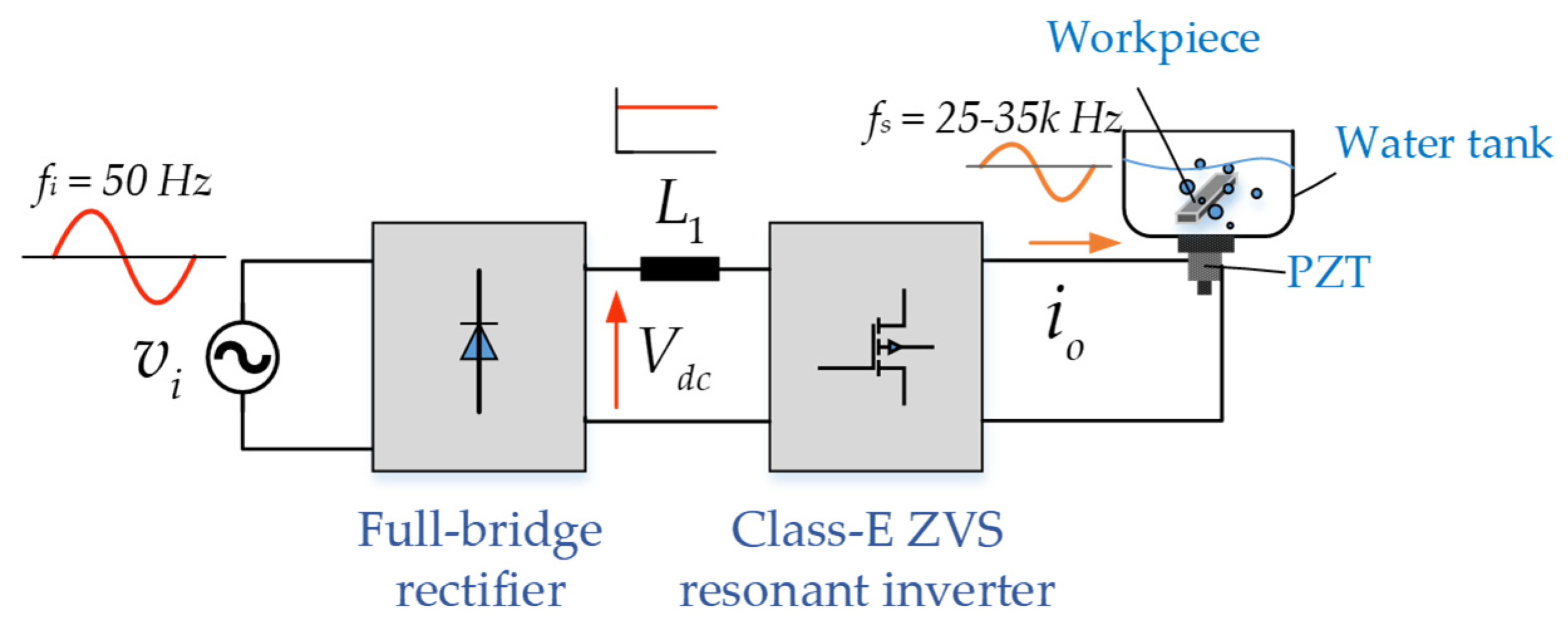
Figure 1. Ultrasonic cleaning system.
Jlpea 15 00054 g001
Figure 2. The Class E ZVS resonant inverter.
Jlpea 15 00054 g002
Figure 3. The ultrasonic piezoceramic transducer: (a) physical structure of the PZT used in the prototype, with a diameter of 5.4 cm and a height of 5.3 cm; (b) a full equivalent circuit model including motional components L m , R m , and C m in parallel with static capacitance C o ; and (c) a simplified steady-state model, where the motional branch is approximated by a parallel combination of C o and R m under resonant conditions.
Jlpea 15 00054 g003
Figure 4. Equivalent circuits: (a) original configuration of CLC filter and PZT; (b) reduction in parallel capacitors C o and C 3 ; (c) transformation of parallel C a and R m into equivalent series components C 2 and C x ; and (d) final series-resonant circuit composed of L 2 , C t , and R x .
Jlpea 15 00054 g004
Figure 5. The equivalent circuit of a Class E ZVS resonant inverter.
Jlpea 15 00054 g005
Figure 6. The key waveforms for a Class E ZVS resonant inverter.
Jlpea 15 00054 g006
Figure 7. The equivalent circuit of a Class E resonant inverter with parasitic resistances.
Jlpea 15 00054 g007
Figure 8. Control diagram of proposed system: (a) resonant frequency tracking controller using PLL control; (b) analog-to-digital converter (ADC) conditioning board; and (c) opto-isolator circuit.
Jlpea 15 00054 g008
Figure 9. The circuit for the zero-crossing detector.
Jlpea 15 00054 g009
Figure 10. Opto-isolation circuit.
Jlpea 15 00054 g010
Figure 11. Algorithm resonant frequency tracking flowchart for Class E resonant inverter using phase-locked loop.
Jlpea 15 00054 g011
Figure 12. A laboratory prototype of the proposed system. (a) The Class E ZVS resonant inverter with the CLC filter. (b) Using the ultrasonic cleaner on the tank.
Jlpea 15 00054 g012
Figure 13. Simulation waveforms of the Class E ZVS resonant inverter at duty D = 0.5: (a) gate–source voltage v g ( Q 1 ) ; (b) switch voltage v D S ( Q 1 ) ; (c) output current i o ; (d) switch current i Q 1 ; (e) output voltage v o ; and (f) shunt capacitor current i C 1 .
Jlpea 15 00054 g013
Figure 14. The non-ZVS operation under load variations.
Jlpea 15 00054 g014
Figure 15. The experimental results of the proposed system at duty D = 0.5: (a) gate–source voltage v g ( Q 1 ) ; (b) switch voltage v D S ( Q 1 ) ; (c) output current i o ; (d) switch current i Q 1 ; (e) output voltage v o ; and (f) shunt capacitor current i C 1 .
Jlpea 15 00054 g015
Figure 16. The experimental results of the proposed system at the duty D = 0.5 under load variations: (a) gate–source voltage v g ( Q 1 ) ; (b) switch voltage v D S ( Q 1 ) ; (c) output current i o ; and (d) switch current.
Jlpea 15 00054 g016
Figure 17. The experimental results of the proposed system at duty D = 0.2 under load variations.
Jlpea 15 00054 g017
Figure 18. Experimental results of power adjustment according to load change in ultrasonic cleaning applications for Class E resonant inverter: (a) voltage waveform v D S ( Q 1 ) and current i o at time scale of 2 s/div; (b) voltage waveform v D S ( Q 1 ) and current i o for power at 100% at time scale of 10 µs/div; and (c) voltage waveform v D S ( Q 1 ) and current i o for power at 40% at time scale of 10 µs/div.
Jlpea 15 00054 g018
Table 1. PZT parameters.
ParametersValueUnit
R m 320.05 Ω
L m 85.25mH
C m 170.15pF
C o 2.52nF
Disclaimer/Publisher’s Note: The statements, opinions and data contained in all publications are solely those of the individual author(s) and contributor(s) and not of MDPI and/or the editor(s). MDPI and/or the editor(s) disclaim responsibility for any injury to people or property resulting from any ideas, methods, instructions or products referred to in the content.