1. Introduction
The junction temperature of devices is of great significance in reliability assessment, such as thermal fatigue degradation and lifespan prediction [
1]. Since measuring the internal junction temperature is nearly impossible, researchers have employed various techniques over the past few decades, such as the finite element method (FEM), thermal parameter extraction methods, and thermal impedance model methods, to extensively study power devices to estimate accurate junction temperature [
2,
3]. Although the FEM can provide relatively precise results, its computational process is time-consuming and requires substantial computational resources [
4,
5]. On the other hand, for the thermal parameter extraction method, a set of measurement process is needed [
6,
7]. In contrast, the thermal impedance model method not only is suitable for predicting dynamic thermal behavior but also can be used for analyzing long-term load profiles, with the merit of less cost [
8]. However, the application of the thermal impedance model requires consideration of coupling effects and heat dissipation boundary conditions [
9,
10,
11,
12].
The thermal coupling effect between the power module chip and the key substrate layers can be characterized with the bypass resistance extracted from the step power response [
13]. The relevant literature shows a method of connecting a voltage source in series with the coupling impedance to establish a three-dimensional RC block thermal model [
14]. However, the process of extracting all coupling impedances is relatively complex and especially unsuitable for multicomponent converters. In practice, the coupling effect of individual devices is varied in different circumstances [
15,
16].
On the other hand, in practical applications of the converters, including photovoltaic inverters, onboard inverters, and wind power converters, the power loss of the modules always exhibits symmetrical distribution of the temperature [
17]. The substrate can be treated as a uniform RC block, which may enable the neglect of boundary conditions for temperature distribution [
18]. The relevant literature changed these boundary conditions by analyzing the shell junction impedance at different positions on the substrate [
19].
In order to simulate the dynamic thermal behavior of power MOSFET modules in the converter, three typical thermal models are usually used, including the numerical model, analytical model, and thermal network model. Numerical simulation is a technique widely used to solve thermodynamic problems with complex geometries and boundary conditions. Commercial thermal simulation software, such as COMSOL 6.3 and ANSYS 10.0/ICEPAK 4.2, provides powerful computational fluid dynamics tools for electronic thermal management. The finite volume method, finite difference method, or finite element method are adopted in the software to solve partial differential equations, which can accurately simulate the actual thermal behavior but with the sacrifice of timeliness. Although the model reduction method can improve the computational efficiency, it often sacrifices a certain accuracy [
20].
The analysis model is based on the thermal diffusion equation with physical meaning to study the thermal behavior of the power module. In order to solve the heat equation, a variety of methods are proposed, including the boundary element method, three-dimensional transmission line matrix method, Green’s equation [
21], Fourier series expansion method [
22], and finite difference method [
23]. The analytical model achieves faster calculation speed by simplifying the actual physical structure, which requires researchers to have a solid mathematical and physical foundation.
Compared with the above two models, the thermal network model is easy to integrate with a circuit simulator and digital signal processor (DSP), and it is especially suitable for long-term load distribution analysis and online temperature estimation [
24]. The reasons are as follows: (1) Model simplification and efficiency: The thermal network can simplify the complex heat transfer process into a relatively simple structure, which makes the model calculation more efficient and maintains high accuracy. Similar to the circuit model, the structure and principle of the thermal network model are similar to a network composed of resistors, capacitors, and other components in a circuit. (2) Modularization and flexibility: The thermal network model can be modularly constructed according to actual needs. Different components or regions can be represented by corresponding thermal network modules, which has high flexibility. (3) Real-time detection and feedback: The thermal network model can calculate and give feedback on the temperature change at each point in the system in real time.
The thermal network model includes the Foster thermal network and Kaur thermal network [
21]. Under certain boundary conditions, the data of the Foster thermal network can be obtained from a data table. However, when the temperature of the reference point changes, the junction temperature in the traditional Foster thermal network is changed synchronously with the reference temperature, which may introduce errors. The traditional Kaur thermal network shows higher accuracy. It is a one-dimensional model that does not consider the thermal coupling effect [
25,
26].
The compact thermal network can reflect the dynamic change in junction temperature more accurately. However, it is challenging to construct a compact thermal network. The extraction of thermal resistance and heat capacity parameters usually depends on the finite element simulation method. The power MOSFET is mainly distributed in the fields of motor drives, new energy vehicle photovoltaics, and so on. As a heating element, the difference between different modules is fitted as the coupled thermal impedance. Therefore, this paper uses the junction temperature change of a power MOSFET in a photovoltaic power module to verify the junction temperature measurement method proposed in this paper. In this paper, an assessment of the coupling degree of the MOSFET module in the photovoltaic power optimizer is conducted, leading to the derivation of a critical coupling impedance matrix. This matrix can be used to decrease the complexity of thermal modeling and enable the accurate estimation of the junction temperature.
Developing compact thermal networks for multichip power modules remains a significant technical challenge. While finite element method (FEM) simulations are conventionally employed for extracting thermal resistance and heat capacity parameters, existing modeling approaches present notable limitations. Schweitzer [
27] demonstrated dynamic compact thermal modeling for multisource semiconductor devices through nonlinear optimization algorithms, but the methodology demands extensive computational iterations to achieve convergence. Bahman et al. [
8] implemented step response analysis to establish 3D lumped thermal models accounting for thermal coupling and boundary conditions, yet their approach exhibits a labor-intensive nature and limited scalability for multichip configurations. Li et al. [
13] developed a three-step curve-fitting method to extract physically meaningful resistor–capacitor (RC) parameters from FEM results, effectively addressing Foster network limitations in multichip applications. However, the substantial parameter space (multiple R and C values) complicates the identification process. To overcome these collective challenges, this work proposes a novel two-step methodology for constructing optimized compact thermal models in multichip power modules.
In this paper, we mainly establish the FEM based on the power MOSFET module in a photovoltaic power enhancer. The correctness of the model is verified by probe detection. The coupling effect between the MOSFET devices and the influence of the boundary conditions on the temperature are analyzed. The results of the thermal network model of the power device are mainly due to the power loss and cooling conditions of the device. In this paper, they are simulated and verified to further improve the correctness of the model. The model-building method in this paper can be used on the power MOSFET devices, which are commonly adopted in the photovoltaic power enhancers. In different application environments, the corresponding thermal network model can be extracted only by modifying the parameters of each material layer in FEM, which simplifies the junction temperature measurement with small error.
2. Heat Distribution Analysis
There are many reports on the thermal modeling of photovoltaic grid-connected inverters and wind power converters [
28]. Most of the converters are designed with integrated modules. In a modular device, the chips are assembled on a PCB substrate so that the heat flow generated by the device junction can be dissipated through the same thermal path, thereby realizing the symmetry of the temperature distribution. In contrast, a photovoltaic power optimizer typically works in conjunction with discrete devices, with their respective substrates at different locations in the radiator [
25]. Because of different cooling paths, the junction temperatures of the power devices are different even under the same thermal load, resulting in uneven heat dissipation distribution [
29,
30].
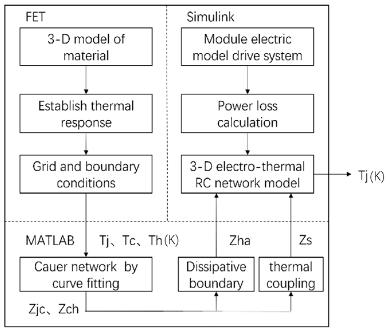
In order to explore the nonuniform heat distribution of the asymmetric photovoltaic power optimizer, the steady-state thermal simulation of the power MOSFET module of a photovoltaic power enhancer is carried out by using the finite element method (FEM). Based on the calculation of power loss, the boundary conditions of the heat dissipation and the coupling effect are studied, and a junction temperature estimation model of the power MOSFET is extracted. The measurement principle is shown in
Figure 1. The input current vin is output through an inductor, resistor, capacitor, 4MOSFET, and Bluetooth module. The thermal modeling process is illustrated in
Figure 2.
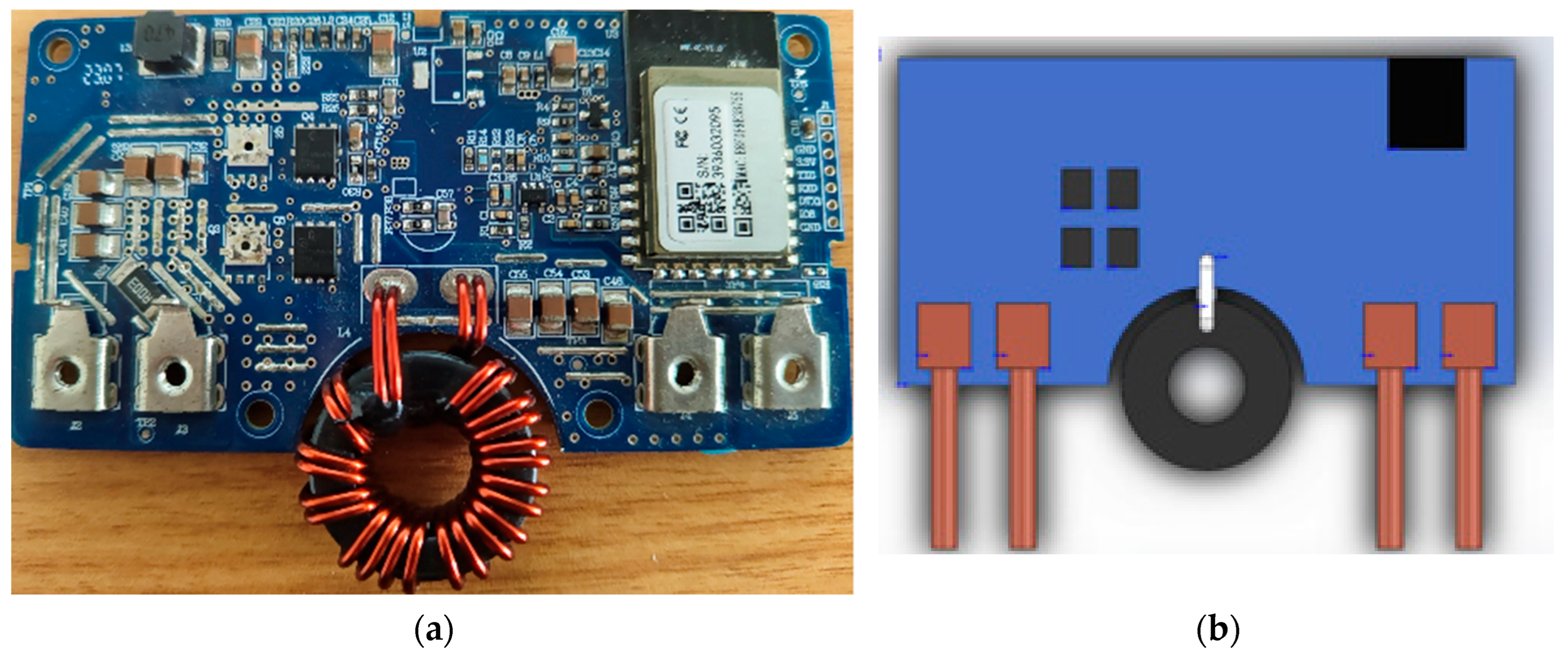
In the photovoltaic power enhancer, a large amount of energy loss is generated by the power module. The thermal dissipation approach for the power module with high power density should be studied carefully. Advanced packaging and heat dissipation technologies can improve the heat dissipation efficiency of the power module. The structure of the photovoltaic optimizer is shown in
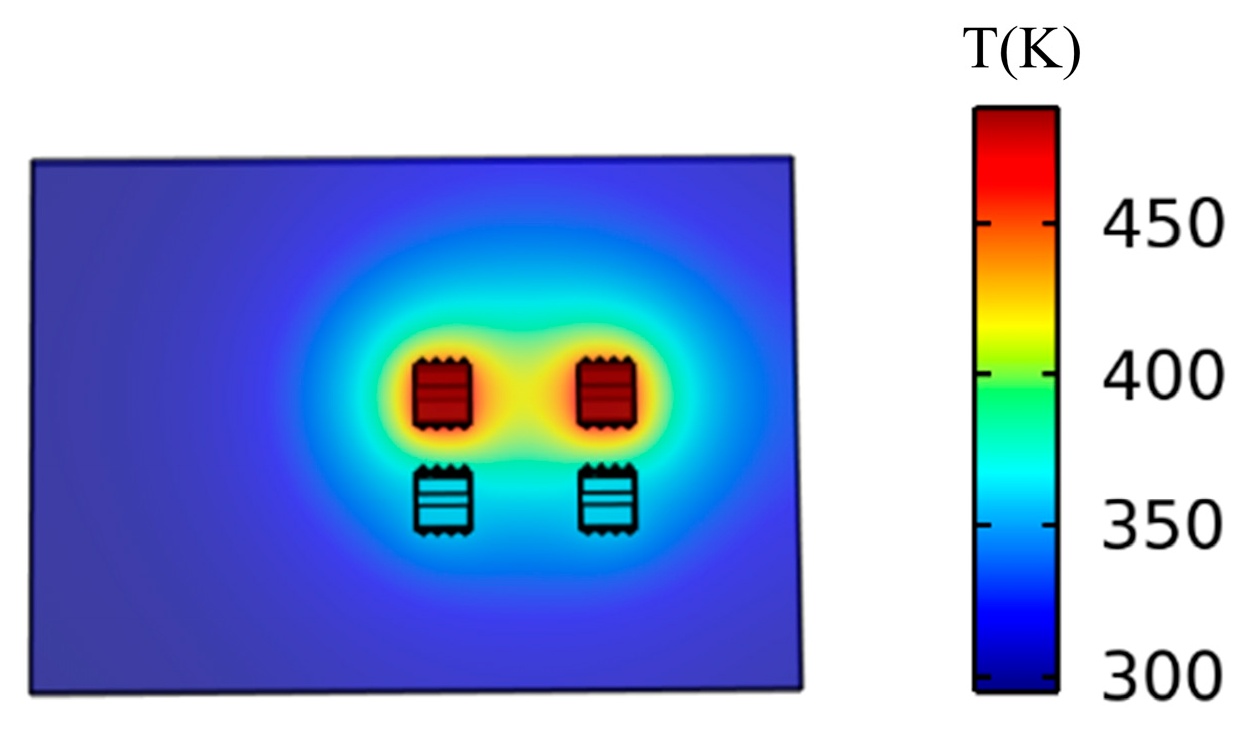
Figure 3. The schematic of the JMSH1004BGQ module is shown in
Figure 4, with the simulation result on the module. In addition, assuming that the ambient temperature is a constant value (20 °C), the convection heat transfer coefficient on the heat-sink surface is set as h = 6.8 × 10
−6 W/(mm·°C) with the emissivity as e = 0.4, and the simulation time is selected as 300 s. And in different applications, as long as the convection of the radiator is modified in comsol, there is no need to redesign the extraction method.
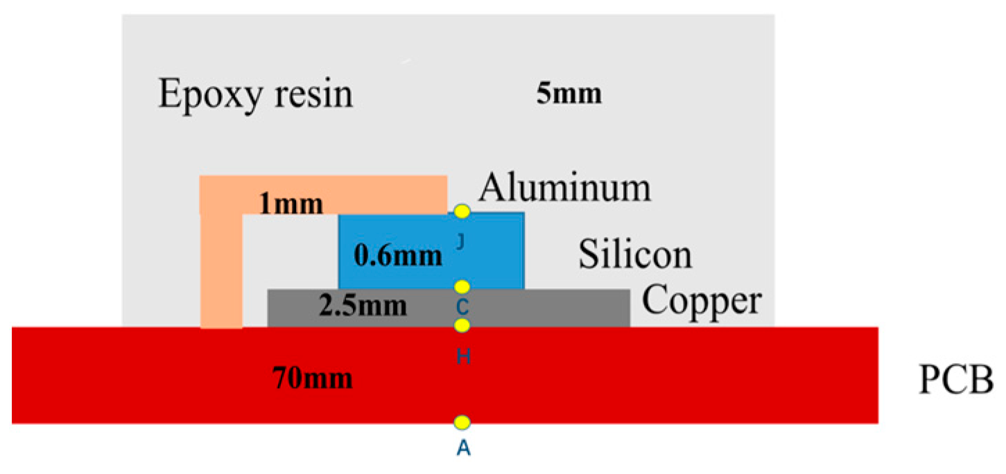
Finite element simulation plays an irreplaceable role in the thermal analysis of photovoltaic power enhancer systems. Thermal behavior can be simulated by a meshing process and setting strict boundary conditions. A MOSFET JMSH1004BGQ (Made by Jie Jie Microelectronics Co., LTD, Suzhou, China) module is taken as the prototype, which is divided into the aluminum electrode layer, silicon chip layer, copper metal layer, epoxy resin layer, and PCB layer, as shown in
Figure 5. The lateral dimensions of different materials are marked: the silicon layer is 0.6 mm, the copper is 2.5 mm, the aluminum is 1 mm, the epitaxial is 5 mm, and the PCB is 70 mm.
As shown in
Table 1, the material properties of the three-dimensional finite element model are listed, including thermal conductivity, specific heat capacity, thickness, etc.
The thermal impedance Z
jc(t) from the junction to the shell as the key layer plays an important role in thermal modeling, which is defined as follows:
where Tj(t) and Tc(t) are expressed with time as the junction and case temperatures of the MOSFETs, respectively, and P
step(t) represents the heat source of the device. Thus, a step power loss is loaded as heat flow on the MOSFET die layer (Node J) in FEM, and the transient temperature Tj(t) and Tc(t) can be obtained by probe.
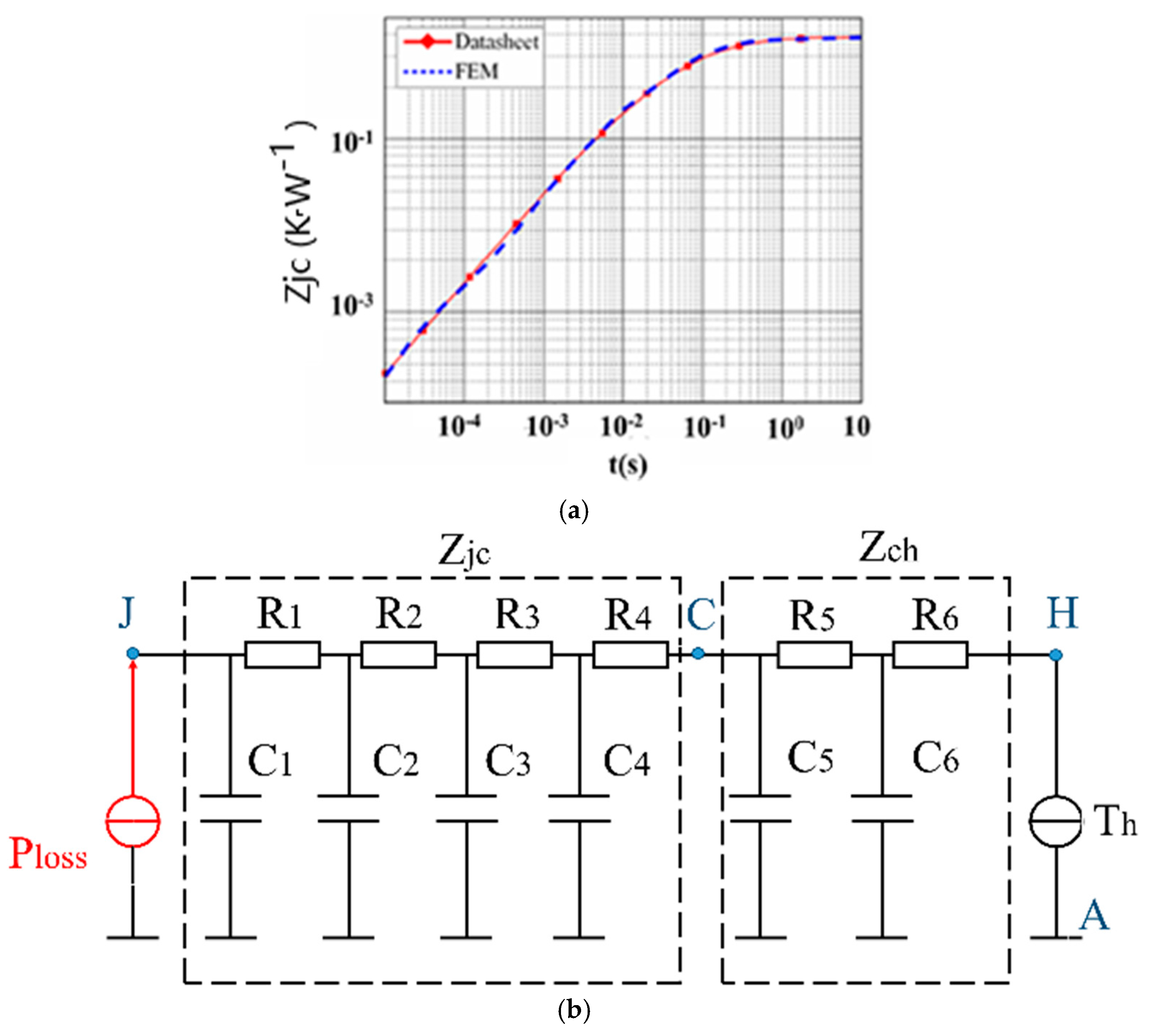
Figure 6a depicts the temperature response result, and FEM results are plotted in log coordinates with dotted lines. It is in good consistency with the datasheet, which indicates that the FEM model established in this paper is certainly effective.
Thermal impedance can be denoted with an RC network, which is mainly divided into the Foster model and Cauer model. The Foster model can be obtained from the step thermal response, but its structure is inconsistent with the physical meaning. The Cauer model can reflect the actual thermal path and has more effective cascade characteristics. In this paper, the Cauer network model is used to represent the heat conduction of the MOSFET, as shown in
Figure 6b. The heat flow generated by the power loss of the device, from the module point J to the chassis node C, is conducted between the inner layers. The heat is dissipated to the environmental node A through the impedance Z
ch of the grease and the radiator, and the temperature is constant at room temperature (20 °C).
In order to describe the thermal impedance in the form of an RC network, Z
jc can be interpreted as
where r
i and c
i are the thermal resistance and heat capacity of the Foster network, respectively.
Using the same method, the thermal response curve of oil impedance Z
ch can be extracted from the finite element method. Then, the Foster network can be converted to the Cauer network for r
i and c
i values. Considering that the time constants of a MOSFET and thermal grease in the step thermal response are different, the Z
jc of a MOSFET device is fitted by the fourth order, and the Z
ch of thermal grease is fitted by the second order to meet the accuracy requirements. The r
i and c
i values of the MOSFET module in the Cauer network are shown in
Table 2.
The radiator is one of the main components on the thermal path from node J to node A, and its heat dissipation characteristics have a decisive influence on the temperature distribution. Studies have shown that when a power device is installed at different positions on the surface of a radiator, the heat dissipation paths may be unequal [
18], which is one of the reasons for the uneven temperature distribution.
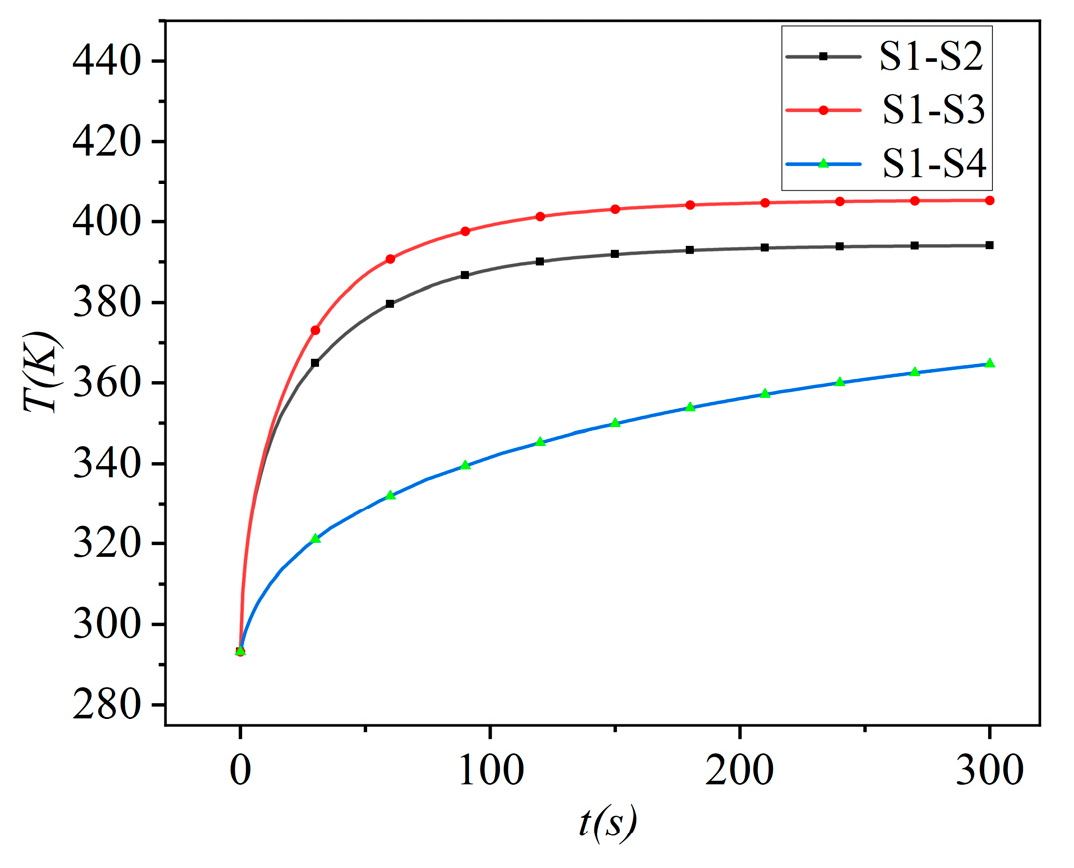
Considering the geometric symmetry of the converter structure, the points (node H) S1, S2, and S3 are defined as three typical positions for analyzing the heat dissipation of the radiator, with the points as shown in
Figure 4. The junction temperature response can be extracted in a FEM simulation by loading the same step power loss on the device at four typical positions, as shown in
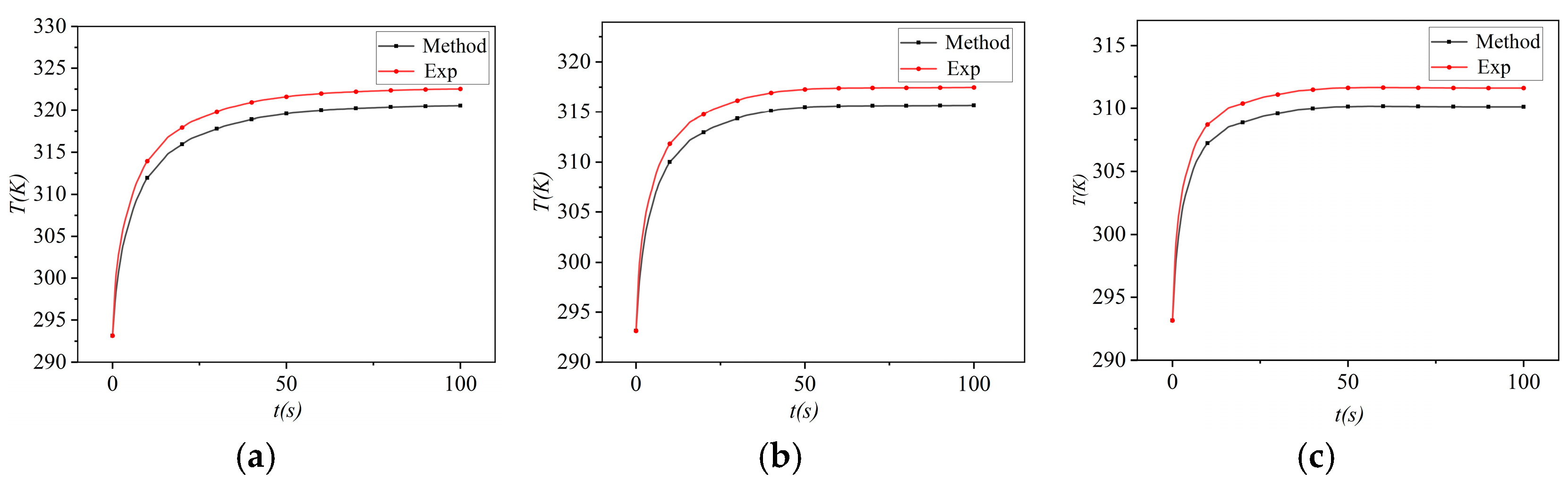
Figure 6. In the case of the same impedance of a MOSFET and grease, the junction temperature curves shown in
Figure 7 are different, especially in the stable state after 90 s, which can only be caused by the uneven dissipation boundary conditions of the radiator.
For a photovoltaic power enhancer, although the power losses of the loads on the same functional devices (such as S1 and S3) are equal, the junction temperature distribution of the devices is not uniform. Therefore, in order to accurately estimate the junction temperature, it is necessary to consider the heat dissipation boundary conditions. The difference between dissipative boundary conditions is mainly reflected in the stable junction temperature and time constant. The stable junction temperature is determined by the thermal conductivity, and the response time constant is affected by the specific heat capacity.
For traditional power converters, such as photovoltaic grid-connected inverters and wind power converters, power losses and thermal circuits are generally symmetrically distributed in an integrated module [
26]. Therefore, in the process of radiator modeling, even if the boundary conditions can be considered, the thermal path is generally regarded as a unified thermal impedance. However, in this paper, a complete radiator is decoupled into multiple sub-radiators for each device. These subdivisions have unequal thermal conductivity and specific heat, so the difference in dissipative boundary conditions can be represented by the corresponding sub-radiators.
For example, Z
ha(S1) and Z
ha(S2) (Z
ha(S1) and Z
ha(S2) are the thermal impedances of the H-A node of the S1 and S2 devices in
Figure 4, respectively) represent the thermal impedances of the sub-radiator below S1 and S2, from node h to a, respectively. According to the thermal response curves of four typical positions, the Cauer RC network of the sub-radiator is extracted by curve fitting in MATLAB 2023. The fitting order can be selected as the second order to meet the accuracy requirements.
Table 2 describes the thermal impedance of the sub-radiator under different boundary conditions at four typical locations.
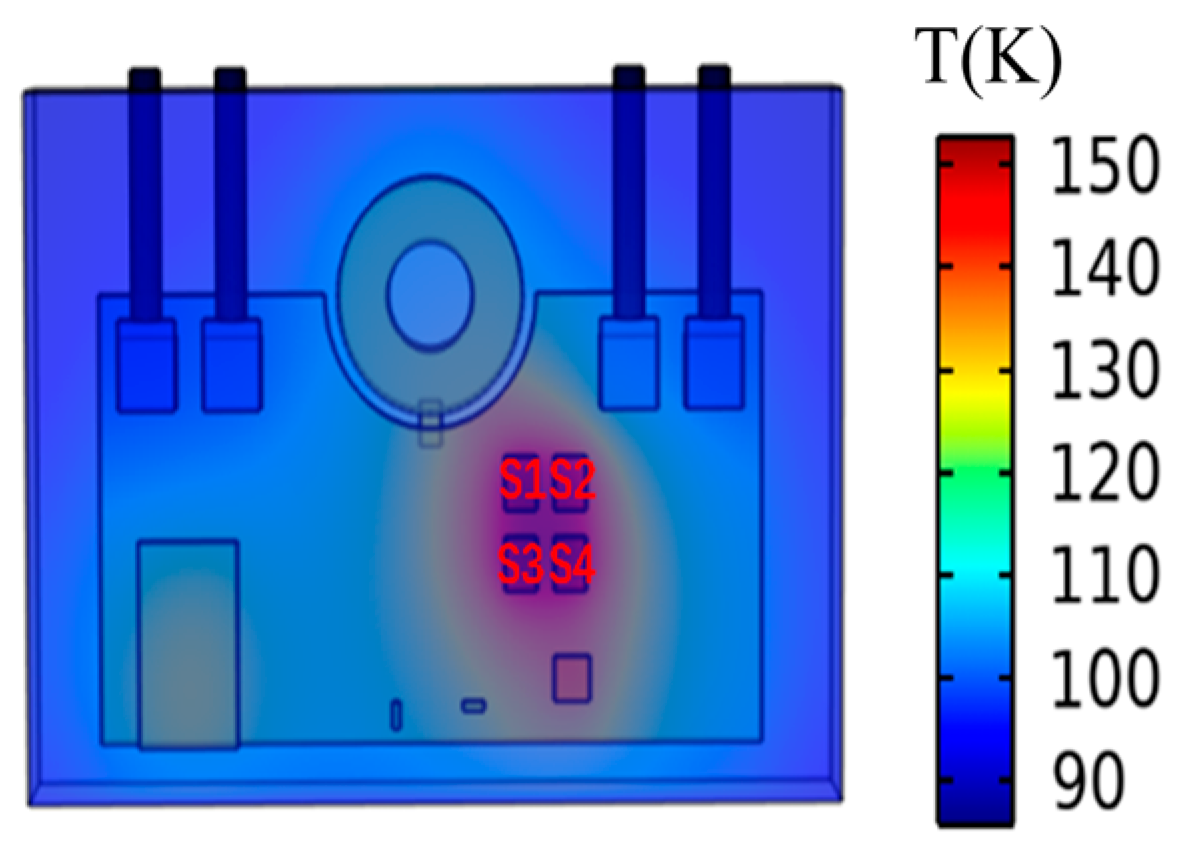
Based on the analysis of power loss and uneven heat dissipation boundary conditions, a set of actual loss distribution values, shown in
Table 1, can be loaded into the FEM to obtain the steady-state temperature of the converter. When multiple components work together, the heat flow generated by the power loss not only causes its own temperature rise but also causes the temperature rise of surrounding devices. The device would be affected by the thermal coupling from other devices. In order to further explore the accurate junction temperature, it is necessary to study the coupling effect of thermal behavior.
Due to the special loss distribution of asymmetric MOSFETs, the coupling effects among devices are different. Therefore, the actual power loss is used in this paper instead of the step thermal response, which can reduce the complexity of thermal modeling and meet the accuracy requirements. When the ambient temperature is 22 °C, the heat transfer coefficient is 3000 W·m
−2·°C
−1, and the Ploss = 1, 1.5, 2 W is applied to the S1 device, the Tj of S1 changes with time as shown in
Figure 8a. When the heat loss is higher, the temperature peak is higher. When the ambient temperature is 22 °C, the heat transfer coefficient is 3000 W·m
−2·°C
−1, and the Ploss = 1 W is applied to the S1 device, the Tj of S1 changes with time at different flow rates of 1.5, 2, and 2.5 m/s, respectively, as shown in
Figure 8b. The larger the flow rate, the lower the temperature peak.
When the simulation of Ploss = 1 W is applied to the S1 and S2 devices at the same time, the stable state is shown in
Figure 9. The two devices are coupled and the peak temperature is greatly improved. When Ploss = 1 W is applied to S1 and S2, respectively; Ploss = 1 W is applied to S1 and S3; and when Ploss = 1 W is applied to S1 and S4, the temperature curve is shown in
Figure 10. The power MOSFET is affected by the coupling effect. The farther the distance is, the smaller the coupling effect is.
3. Loss Model and Heat Network Model
As the input of the heating network, including conduction loss and switching loss, the power loss includes the following parts.
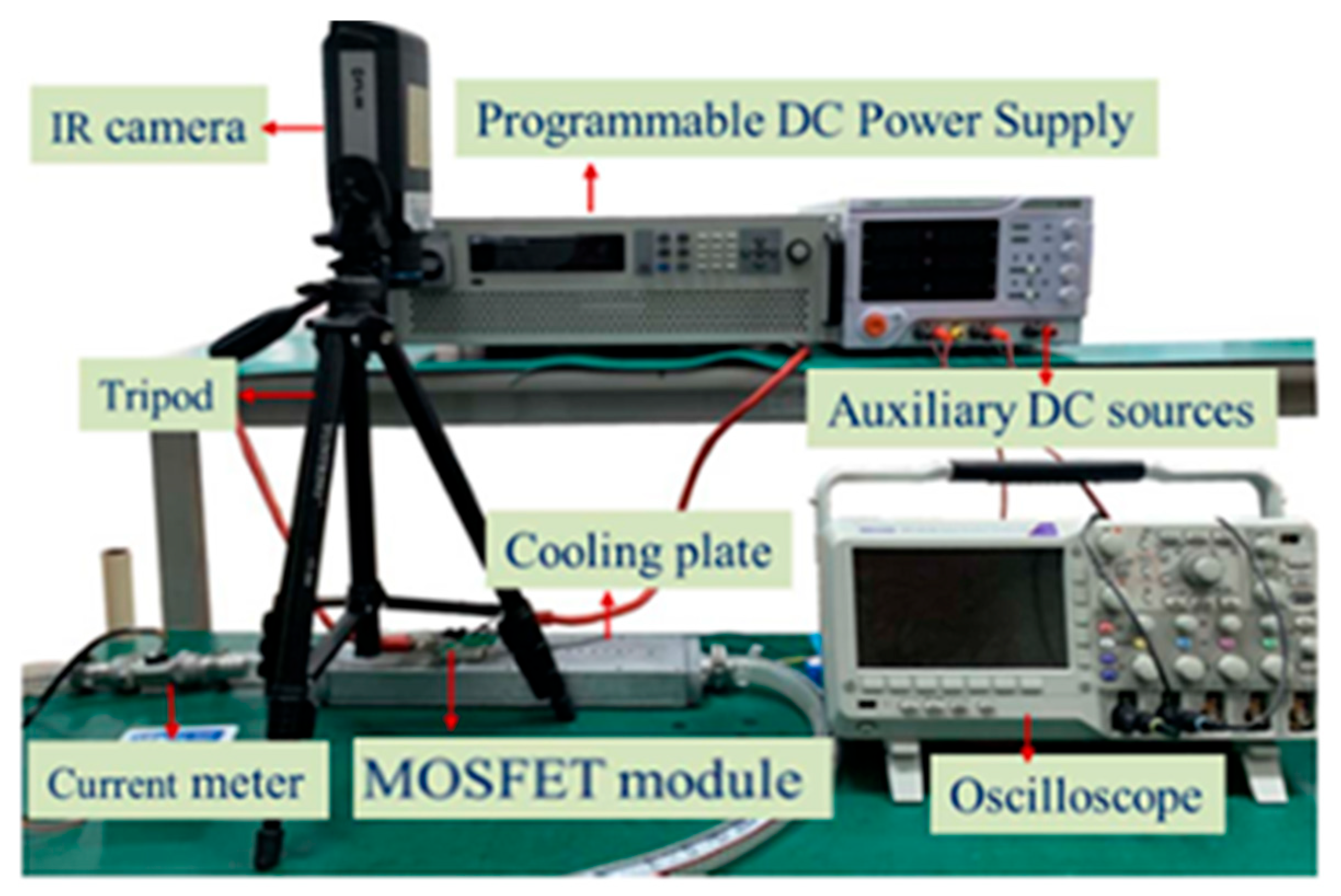
Firstly, switching loss should be considered. The switching loss in a MOSFET includes conduction loss and turn-off loss, while the switching loss in a diode is given by recovery loss. Compared with conduction loss, the switching loss is closely related to many variables, such as DC bus voltage, current, junction temperature, gate drive resistance, and voltage. A double pulse test is carried out to calibrate the switching loss under different working conditions. In the actual switching loss measurement, the switching energy can be obtained by the integral function of the digital oscilloscope.
The second part is conduction loss. In an electrical excitation cycle, the junction temperature fluctuation of the power module cannot be ignored. Therefore, a model of average conduction loss in a period is established [
28,
29,
30,
31,
32].
In order to understand the junction temperature estimation approach, a three-dimensional compact RC network model of an asymmetric power MOSFET for a photovoltaic power optimizer is proposed in this paper [
25,
33,
34]. The model can reflect the nonuniform distribution of power loss and can be used to estimate the heat dissipation boundary conditions and thermal coupling effects. However, the junction temperature should be regarded as the superposition result of temperature rise caused by self-loss and coupling effect under different dissipative boundary conditions.
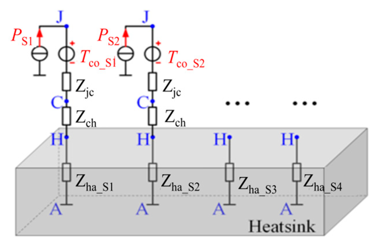
Figure 11 shows the RC network model.
As shown in
Figure 11, the current source presents the heat flow generated by the power loss of the device itself. The thermal impedance Z
jc and silicon grease Z
ch of the device are arranged on the surface of the radiator in turn, forming a thermal path from node J to node A. In contrast, the thermal coupling effect is modeled as a voltage source between the insertion node J and the impedance Z
jc, and the magnitude of the source voltage is controlled by the degree of the coupling effect of other devices. In the model, various dissipative boundary conditions are expressed as four typical sub-radiator impedances connected in series at the end of the thermal path and exposed to ambient temperature.


