Article

An Ultra-Low-Power 0.8 V, 60 nW Temperature Sensor for Battery-Less Wireless Sensor Networks

Department of Electrical Engineering and Computer Science, University of Arkansas, Fayetteville, AR 72701, USA
*
Author to whom correspondence should be addressed.
J. Low Power Electron. Appl. 2025, 15(1), 1; https://doi.org/10.3390/jlpea15010001
Submission received: 21 November 2024 / Revised: 27 December 2024 / Accepted: 5 January 2025 / Published: 9 January 2025

Abstract

:
This work presents a nano-watt digital output temperature sensor featuring a supply-insensitive, self-biased current source. Second-order temperature dependencies of the MOS diode are canceled to produce a stable reference and a linear temperature-sensitive voltage. The sensor integrates a sensing unit, voltage-controlled differential ring oscillators, and a low-power frequency-to-digital converter, utilizing a resistor-less design to minimize power and area. The delay element in the ring oscillator reduces stage count, improving noise performance and compactness. Fabricated in 65 nm CMOS, the sensor occupies 0.02 mm2 and consumes 60 nW at 25 °C and 0.8 V. Measurements show an inaccuracy of +1.5/−1.6 °C from −20 °C to 120 °C after two-point calibration, with a resolution of 0.2 °C (rms) and a resolution FoM of 0.022 nJ·K−2. Consuming 0.55 nJ per conversion with a 9.2 ms conversion time, the sensor was tested in a battery-less wireless sensor node, demonstrating its suitability for wireless sensing systems.

1. Introduction

In the last decade, battery-less and wireless sensors have enabled large-scale, energy-efficient, and cost-effective monitoring systems. The rapid expansion of wireless sensor networks (WSNs) and the Internet of Things (IoT) has driven the demand for self-powered sensors reliant on environmental energy harvesting. Temperature sensors, widely used in industries such as farming, healthcare, supply chain, climate monitoring, smart homes, and automation [1,2,3], are increasingly required to function in remote and challenging environments, making high-accuracy, area-efficient, and low-power designs crucial [1,2].
Designing ultra-low-power temperature sensors for battery-less systems poses challenges, including efficient energy use to handle intermittent harvesting [4], maintaining accuracy across wide temperature ranges without regular calibration [5], and compact designs for cost-effective mass production. Fully integrated sensors must also generate all biases internally, removing reliance on external references.
A wide range of temperature sensors have been developed using CMOS technology [6], employing bipolar junction transistors (BJTs) [7,8,9], resistors [10,11], or MOSFETs [12,13,14]. BJT-based sensors leverage the complementary-to-absolute-temperature (CTAT) behavior of the base-emitter voltage (VBE) and the proportional-to-absolute-temperature (PTAT) difference (ΔVBE) between transistors with varying current densities to generate a temperature-insensitive reference voltage [9]. Accurate digital measurements are achieved by comparing this reference voltage with the PTAT voltage using an analog to digital converter (ADC) [8,15]. While BJTs provide a wide sensing range (−55 °C to 125 °C), they face challenges like limited dynamic range [16], non-linearity at high temperatures [7,9], and sensitivity to process variations, which can lead to errors mitigated by one-point calibration (±0.1 °C) [17]. Their high turn-on voltage (>0.7 V) and µW-level power consumption make them unsuitable for low-power, battery-less applications [8].
Resistor-based temperature sensors provide low power consumption, linear responses, and simple designs, but are prone to self-heating inaccuracies [18] and high process sensitivity, often requiring 2-point calibration [11]. They can operate across wide temperature ranges (−55 °C to 125 °C) [10] using Wheatstone bridge configurations with resistors of opposite temperature coefficients. However, the process sensitivity of on-chip resistors’ temperature coefficients limits their suitability for many applications [19].
Voltage references using 2T and 4T structures [20] use MOS threshold and thermal voltages (VT) for low power consumption (~pWs) but require special common-mode voltage considerations for o-perational transconductance amplifiers (OTAs). Another design introduces voltage reference and dummy structures to address these requirements, albeit with increased complexity [21]. Resistor-based PTAT and reference current generation demand large resistors (~7 MΩ), which consume significant chip area (42%) and limit integration.
Efforts to reduce power consumption and supply voltage include resistorless current [22] and voltage [23] references consuming under 50 nW and <1 V, respectively. Frequency-to-digital converters, while advantageous, require a reference clock, which may not be available in wireless systems and can increase power consumption. Leakage-dominated ring oscillator (LDRO) sensors [24] offer low power (9.3 µW) and modest accuracy (±0.7 °C from −40 to 125 °C) but depend on external clocks. Time-domain sensors [14] with on-chip clocks achieve lower power consumption (196 nW at 0.95 V). However, many of these designs rely on multiple current sources or large resistors, limiting their integration efficiency and often requiring external references. In contrast, our work introduces a single-branch resistorless approach that significantly reduces both power and area overheads, eliminates the need for external references, and enables fully integrated, battery-less operation.
This work introduces a resistorless, fully integrated MOSFET-based temperature sensor. It employs a single current source to generate temperature-sensitive and reference voltages, using voltage-controlled, current-starved VCOs for digital temperature measurement. A modified Oguey current source [25]—featuring improved supply rejection through active control of internal node voltages—generates all bias currents, enabling low-power operation. Additionally, we adopt a differential pair structure in the ring oscillator to improve noise immunity and achieve a wide tuning range at low supply voltages. Fabricated in a 65 nm CMOS process, the sensor occupies 0.02 mm2, consumes 60 nW at 0.8 V, and achieves ±1.5/−1.6 °C inaccuracy (3σ) from −20 to 120 °C with 2-point calibration, covering a 140 °C span. It offers a 0.2 °C (rms) resolution with a resolution FoM of 0.022 nJ·K−2, consuming 0.54 nJ per conversion over a 9.2 ms conversion time. Although this broad temperature range and short conversion time can introduce challenges for maintaining uniform accuracy, the sensor remains competitive for battery-less IoT applications due to its extremely low power consumption and small footprint.
This paper is structured as follows. Section 2 discusses the architecture of the proposed sensor and provides a mathematical analysis and detailed design of all the functional blocks. Section 3 presents post-silicon measurement results. Section 4 describes the integration of the temperature sensor in a battery-less wireless sensor node. Section 5 concludes the paper.

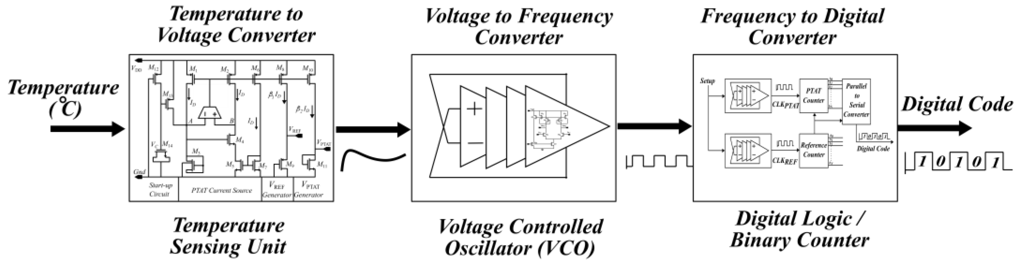
2. Architecture of the Proposed Temperature Sensor

A temperature sensor detects the ambient temperature and converts it into a digital code. Figure 1 illustrates the proposed architecture of this sensor with three main functional blocks: (1) a temperature sensing unit, (2) a voltage-to-frequency converter, and (3) frequency-to-digital converter logic.
The temperature sensing unit produces a PVT-tolerant reference voltage (VREF) and a temperature-sensitive voltage (VPTAT), which controls a VCO to create a temperature-dependent frequency (FPTAT). A second VCO generates a reference frequency (FREF) from the VREF. A digital logic circuit then compares the FREF and FPTAT frequencies to produce a binary temperature code.
To achieve low power consumption (nano-watt) in each block, special design considerations are necessary, particularly in the temperature sensing unit. The voltage ranges of the VPTAT and VREF determine the oscillation frequency range, directly impacting the dynamic power consumption of the digital logic. Therefore, it is critical to have a strictly defined range for the generated voltages in all the process, temperature, and supply corners.

2.1. Temperature Sensing Unit

The temperature sensing unit outputs VPTAT and VREF voltages. Figure 2 shows a conventional way to generate such voltages using a couple of current sources and resistors. While this method is simple, it has limitations. To achieve low-power operation, a low VCO frequency is desired, requiring a low control voltage (~200 mV). If the current source outputs <10 nA, the resistor must be very large (>5 MΩ). Reducing the resistor size requires higher current, creating a trade-off between power and area. This design challenge arises from balancing power efficiency and minimizing area.
A key challenge in the conventional approach is the need for current sources with well-defined PVT dependencies to maintain the linearity of resistors, requiring two sources with different temperature dependencies to generate VPTAT and VREF. This increases design complexity and strains power and area. To address this, we propose a resistorless design (Figure 3) using a single current source with a square temperature dependency (PTAT)2. The current is copied to a branch with a diode-connected MOSFET whose second-order non-linearities are compensated by the square temperature dependency, resulting in linear VPTAT and stable VREF. This design reduces power consumption by 25% (eliminating one of the current-carrying branches) and saves chip area by removing bulky resistors. The use of a single current source ensures identical process variations for both control voltages, simplifying cancellation in the frequency-to-digital converter.

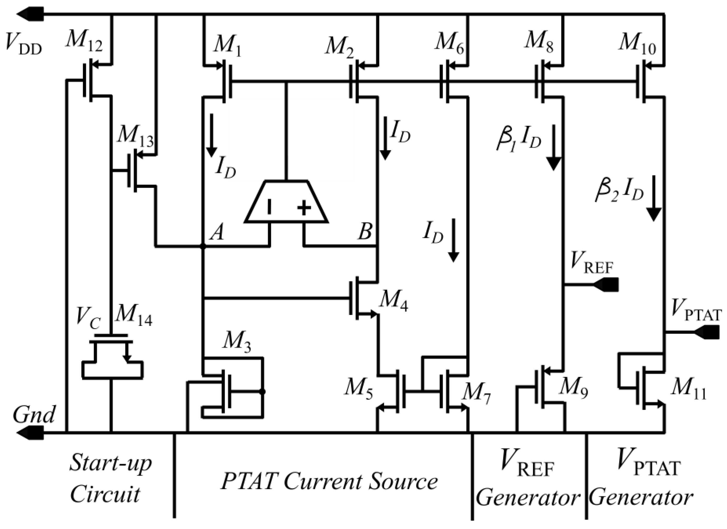
2.1.1. Temperature Sensing Circuit

As mentioned in the previous section, the voltages VPTAT and VREF are generated by passing a bias current (ID) through a diode-connected MOSFET operating in the subthreshold region. The drain current of a diode-connected MOSFET in subthreshold is expressed as [26]:
I D = W L µ C o x V T 2   e x p V G S V T H η V T 1 exp V D S V T
where W/L is the width-to-length ratio of the MOSFET, µ is the carrier mobility, Cox = ɛox/tox is the gate oxide capacitance per unit area, tox is the oxide thickness, and ɛox is the oxide permittivity. VT is the thermal voltage, which is denoted by VT = KT/q, where K is the Boltzmann Constant, T the temperature, and q the charge of an electron. VGS denotes the gate-source voltage of the MOSFET, VTH is the threshold voltage of the MOSFET, and η is the subthreshold slope factor. VDS is the drain-to-source voltage drop.
The size of the MOSFET is kept such that VDS ≥ 4 VT, which is necessary to keep a subthreshold MOSFET in saturation. Setting VDS ≥ 4 VT, (1) can be solved and expressed in terms of the VGS (MOS diode drop) as:
V G S = η   V T ln I D W L µ C o x V T 2 + V T H  
In (2) VT has a positive temperature coefficient (TC), while µ and VTH have a negative TC. These temperature-dependent coefficients can set the temperature behavior of the diode drop if the ID is of the form:
I D = β µ C o x V T 2
where β is an arbitrary variable. The mobility that is a process/temperature term is canceled out, and as a result, better process tolerance is achieved. Note that the current ID in (3) should have a square dependency on the temperature to effectively cancel out the nonlinear term in (2). Substituting (3) in (2) gives:
V D S = V G S = η V T   l n β W L + V T H  
The value of the β variable, the sizing, and the choice of the MOS diode with a suitable temperature dependence can be used to generate VPTAT and VREF, as illustrated in Figure 3. The value of the subthreshold slope factor (η) is about 1.3, and the thermal voltage VT has a well-defined temperature coefficient (TC) of 0.086 mV/K. The threshold voltages (VTH) have a negative TC of −4 to −2 mV/K, which varies from device to device. The temperature coefficient of VT is significantly weaker than that of VTH; thus, to compensate for the negative TC of VTH, a high value of the β/(W/L) >> 1 is needed. After determining the MOSFET size and value of β of the current source, an appropriate choice of MOS diodes is used to generate VPTAT and VREF. A PMOS diode tends to have a more significant temperature dependence in terms of VTH compared to the NMOS diode; hence, a PMOS diode is used to generate VREF, and an NMOS diode is used to generate VPTAT. VTH is the only process-dependent term remaining in (4), but since both the VPTAT and VREF are simultaneously influenced by this variation, it can easily be nullified in the digital logic when comparing the frequencies of their VCOs.

2.1.2. Current Source Design

As we established by the mathematical representation in (3), we require a current source that has a square dependency on the absolute temperature. The current source must be self-biased, low voltage, and immune to supply variation. To meet all those requirements, we present the design of a current source based on Oguey’s topology. The design has been optimized to improve the power supply rejection ratio (PSRR). The Oguey current reference [25] is based on a PTAT current source shown in Figure 4.
The design achieves low-power operation by keeping M3 and M4 in the subthreshold region. M1 and M2 act as current mirrors. The voltage across the resistor determines the magnitude of the current, which is given by:
V S 4 = V T   l n k 4 k 1 k 3 k 2  
where VT is the thermal voltage and k1, k2, k3 and k4, respectively, are dimensions (W/L) of the MOSFETs. It shows that the voltage across the resistor is PTAT because of its dependence on thermal voltages. The voltage remains insensitive to supply variation as long as the voltage drop across M3 remains greater than 4 VT, keeping M3 and M4 in saturation. Oguey eliminates a major drawback from the design by replacing the resistor with a MOSFET (M5) working in the triode region (linear region). A branch is introduced in the circuit to supply bias M5, as shown in Figure 5.
M5 determines the bias current ID, which is kept in the deep-triode region (i.e., the VDS of M5 is much less than its overdrive voltage (VGS − VTH). The current flowing in M5 can be expressed as:
I D = µ C o x k 5   V G 5 V T H 5 V D S 5 1 2 V D S 2
and the voltage VDS5 = VGS3 − VGS4 can be expressed as [25]:
V D S 5 = η V T   l n k 4 k 3
where Kn is the W/L ratio of the nth MOSFET. The MOSFET M7 is diode-connected and operates in saturation. Its current can be expressed as:
I D 7 = 1 2 µ C o x   k 7   V T H V T H 2    
Equations (6)–(8) can be solved to give the current ID as:
I D = 1 2 µ C o x   k 7   V T 2   K e f f
with:
K e f f = S 2   1 2 + S 2 S 2 1 ln 2 S 1
where:
S 1 = k 4 k 3               ,           S 1 = Q k 5 k 7   .
The current ID in (9) is proportional to the square of absolute temperature and the carrier mobility (µ), which meets all the requirements of ID shown in (3). The factor Keff is a function of device sizes and, therefore, can easily be adjusted for (3).
Keeping the NMOS pair (M3 and M4) in the subthreshold region is crucial to ensure insensitivity to supply variation. We propose modifying the Oguey current source to improve the supply rejection by actively controlling the voltage of nodes A and B, as shown in Figure 6. An operational transconductance amplifier (OTA) is used to form a closed loop around nodes A and B with VDD [23]. The OTA gets its bias current from the same current generator block. The OTA is biased at only 2.5 nA to keep the power consumption low. The OTA controls the voltages of nodes A and B so that the change in supply voltage can be directed to the drain-source voltages of M1 and M2, keeping a constant drop across the M3 and M4. When the VDD variation causes the voltage of node B to increase, the input to the non-inverting terminal of the OTA increases, which causes the output of the OTA to rise. This increase in the output of the OTA decreases VGS2 and causes an increase in VDS2, and the voltage of node B falls again and vice versa. It can also be seen in Figure 6 that the OTA creates a virtual short between nodes A and B. These nodes define VDS2, and thus, virtual shorting together the drain and source terminal of M4 makes it diode connected, keeping it in saturation. Node A, however, is connected to the inverting terminal of the OTA and does not benefit from the closed loop. We also replaced the diode-connected MOS (M3) with PMOS-based N-well diodes to achieve improved voltage regulation at node A, further enhancing PSRR. The N-Well diodes are formed by connecting the drain, source, and gate terminal of M3 and utilizing the P-N junctions formed between the N-well (body connection) and the source/drain terminals of the PMOS, as shown in Figure 7. As compared to the original diode-connected MOS in the Oguey current source, the N-Well diodes formed in M3 exhibit a superior voltage regulation across it [27]. By keeping a constant voltage drop at node A, the overall line sensitivity of the generated current is improved. The channel length of the PMOS current mirrors (M1, M2, M6, M8, and M10) are kept long to maintain a high output impedance that provides passive immunity to supply variation, and using long channel length prevents second-order effects like channel length modulation.
The current source is self-biased, so during the power-up, the circuit can settle in two possible stable states. One of the stable states is when the bias current ID is zero, while the other possible state is when ID is of the form in (9). A start-up circuit is introduced in the modified source to prevent the zero-bias current state, as shown in Figure 6. The start-up circuit is simple and comprises M12, M13, and M14. M14 is connected in a MOS-CAP configuration and serves as a delay element keeping M12 and M13 from turning off during the startup. At startup (t = 0), the node voltage VC is zero and transistors M12 and M13 are turned on in strong inversion. The MOS-CAP M14 starts charging through M12 until its voltage reaches up to the supply voltage VDD, causing M12 and M13 to eventually turn off. During startup, M13 ensures that the current source is in a stable state with a finite current flowing in its branches. The start-up circuit consumes power only during a short duration of start-up time. The complete design of the proposed temperature sensing unit is shown in Figure 6. Both M9 and M7 are diode-connected as previously established.
Figure 8 and Figure 9 show the simulation results of VREF and VPTAT across the process corners. The sensing unit consumes 15 nW at 25 °C and achieves a low variability across process corners.

2.2. Voltage-to-Frequency Converter

The voltages from the temperature sensing unit are translated into frequency using a voltage-controlled ring oscillator (VCO). The design of the differential delay element for the proposed VCO is shown in Figure 10. Instead of relying on a conventional approach of using an inverter as a delay element, our work proposes a new differential pair to control the frequency of the ring oscillator. In our approach, the tail current and an extra active load are varied using the control voltage. This variation provides better control and a wide frequency variation with a small change in control voltages. Differential circuits provide good rejection of common-mode supply and substrate noise. Noise sensitivity is a crucial aspect of the design of our temperature sensor; hence, the differential structure of the delay element is a preferable choice to improve noise immunity. In addition to being noise-tolerant, differential ring oscillators also let us employ an even number of stages in the oscillator’s loop. If we want oscillations using single-ended inverters, the stages must be in odd numbers. In our design, we use four differential stages and obtain the necessary inversion by crossing outputs between stages.
As shown in Figure 11, the propagation delay (td) of a single differential stage can be estimated using a simple RC model. The simple RC model is driven from the half-circuit small-signal model during the low-to-high transition, and it can be mathematically expressed as:
t d = C T R T
with RT approximately
R T 1 G m = 1 g m 1 + g m 2
t d = C T G m
where CT is the total load capacitance seen by the output of a stage (including parasitic capacitances) and gm1 and gm2 are the transconductance of M1 and M2, respectively. It can be noted that variation of the active load M1 using the control voltages changes the delay of each stage.
The time it takes for a single transition to propagate twice around the ring of the oscillator determines its oscillation frequency. From [28] the frequency of oscillation FOSC can be expressed as:
F O S C = 1 2 N t d = G m 2 N C T
The outputs VPTAT and VREF from the sensing unit control the frequency of their respective ring oscillators, giving us FPTAT and FREF. It can be noted that the delay of the differential stage depends on transconductance (Gm), and Gm is sensitive to both temperature and supply voltage. The ring oscillator with fixed control voltage shows a simulated supply sensitivity of +1.1 to −1.8 °C (temperature reading error) across a supply variation of 0.8 to 1.4 V and a mean temperature coefficient of 85 ppm/°C. Although the ring oscillator is sensitive to both supply and temperature variations, we mitigate these issues by comparing the two frequencies in the digital section, which cancels much of the common-mode drift. The temperature sensing accuracy may also suffer due to process variation; therefore, careful layout considerations are adopted to minimize this variation. Long-channel devices are used along with common centroid layouts to minimize mismatches.

2.3. Frequency-to-Digital Converter

A digital logic circuit is designed to convert the frequencies FPTAT and FREF into digital outputs using two asynchronous counters configured as 12-bit binary counters. FPTAT and FREF serve as the clock sources ClkPTAT and ClkREF for the PTAT- counter and reference counter, respectively. The frequencies are chosen such that the reference frequency is always greater than the PTAT frequency at all temperature, supply, and process corners. As shown in Figure 12, the ‘Setup’ signal triggers the oscillation in both oscillators and resets the counters, making them increment with each clock pulse. Since the reference frequency is higher, its counter overflows first, raising its ‘overflow’ signal. This overflow signal triggers the transfer of the count from the PTAT counter to the parallel-to-serial converter. To prevent metastability, we introduce a short chain of inverters/buffers after the PTAT counter stops, ensuring its output stabilizes before latching. The ‘Setup’ signal then clears and starts both counters again for a new temperature reading. At high temperatures, more counts are accumulated in the PTAT counter, and at low temperatures, the accumulated count is low. Hence, the PTAT count serves as the binary representation of the measured temperature. Conversion can be set to continuous mode using the internal ‘Setup’ signal or, to conserve power, the conversion can be triggered from an external signal when needed. Circuit level optimization is achieved by carefully considering the device sizing in each switching stage of the counters to minimize short circuit currents and leakages. We use only one differential output of the final (fourth) VCO stage to clock each counter, simplifying the clock distribution. Capacitive loading of the counter is also minimized at the layout level to reduce the charging and discharging currents, leading to efficient power consumption.

3. Experimental Results

The micrograph of the temperature sensor chip is shown in Figure 13. The design is fabricated in a 65 nm CMOS process and occupies an area of 0.02 mm2.
The measurement setup is shown in Figure 14. Twelve dies were selected and packaged in a QFP package to test the temperature sensor.
Figure 15 shows the output voltage VPTAT over the range of −20 to 120 °C. The VPTAT output shows a linear output with minimal dependence on process variation. The average temperature sensitivity of VPTAT was measured to be 0.19 mV/°C. A mean value of 266.4 mV was observed at a supply voltage of 0.8 V @ 25 °C, with a standard deviation of 13.19 mV across samples. The output voltage VREF is shown in Figure 12. VREF showed an average temperature sensitivity of 0.95 µV/°C, and a mean value of 601.5 mV was observed at 0.8 V supply @ 25 °C. VREF showed a standard deviation of 25 mV across samples.
The average power consumption of the sensing unit was measured to be 18 nW. The measured average FPTAT varied from 168 KHz to 308 KHz across the temperature range, and the measured average FREF was 442 KHz @ 25 °C, as shown in Figure 16.
The average RMS resolution of the temperature sensor across samples was measured to be 0.2 °Crms. The resolution showed an inverse relation with conversion time, as shown in Figure 17; however, this improvement in resolution increased the energy expenditure per conversion.
A supply voltage change from 0.8 to1.2 V produced an error of +1.5/−2.1 °C in the temperature measurement. Figure 18 shows the measured error of 1.5 °C/−1.6 °C across the temperature range after 2-point calibration at 25 °C and 105 °C.
The average power consumption of the complete sensor over the 12 dies at ambient temperature, and 0.8 V supply is 59 nW. The overall power breakdown is shown in Figure 19, which shows that the ring oscillator accounts for about 50% of the power consumption while generating VREF, and VPTAT consumes about 30% of the total power budget.
Table 1 shows the comparison of the design with other low-power temperature sensors reported in the literature. The comparison is based on a figure of merit (FoM) derived from [6]. A lower FoM means better performance and is calculated as follows:
F o M n J . K 2 = E n e r g y / C o n v × R e s o l u t i o n 2
Different process nodes (e.g., 180 nm vs. 65 nm) significantly impact achievable accuracy, power, and supply voltage ranges. Although some sensors in Table 1 achieve slightly tighter accuracy, they often operate over narrower temperature spans or at longer conversion times, thereby trading off speed or range for accuracy. The design in [30] achieves the lowest energy per conversion due to its reduced power and short conversion time, yet it exhibits the highest inaccuracy among the compared solutions. In comparison, our sensor covers a larger temperature range, −20 to 120 °C, and uses only 9.2 ms conversion time, balancing power efficiency with operational speed while still achieving a moderate inaccuracy level. We also employ two-point calibration, which is standard in many reported designs. Notably, only [29] demonstrates a better FoM due to its higher resolution, but it requires a higher supply voltage than the other references. By contrast, our proposed design offers significantly better performance in terms of area, supply voltage, conversion time, and energy per conversion. Future improvements may include exploring single-point calibration or advanced process compensation to further reduce calibration overhead and improve accuracy.

4. Integration with the Wireless Sensor Node

A wireless-powered sensing node is fabricated separately to integrate with our proposed temperature sensor. The goal is to achieve a fully integrated ultra-low-power wireless temperature sensor node. Figure 20 shows the block diagram of the WSN and its integration with the temperature sensor. The WSN works by harvesting power from the ISM band (915 MHz). The system operates in a cycle of two phases. During phase I, the antenna is connected to an RF rectifier through an RF switch. The transmitter and the temperature sensor are in sleep mode during phase I to conserve power. The harvested power is stored in an external storage capacitor. As soon as the voltage on the storage capacitor reaches a specific threshold, the power management circuit switches the RF switch and wakes up the temperature sensor and transmission circuit. During phase II, the 915 MHz signal is directed to the carrier extractor and frequency synthesizer through the RF switch. The carrier extractor boosts the amplitude of the received 915 MHz and divides it by a factor of 3 to down-convert it to a 305 MHz square signal. The down-converted signal then goes through an 8× frequency multiplier, resulting in a 2.44 GHz signal that is suitable to be used as the carrier for ISM band transmission. The 2.44 GHz signal is modulated using the on–off keying (OOK) scheme by the serial data coming from our proposed temperature sensor. Finally, a power amplifier transmits the modulated signal.
The temperature sensor was tested after integration in WSN. The measurement results showed a degradation in temperature measurement accuracy with an error of 1.8 °C/−2.1 °C across the temperature range after 2-point calibration at 25 °C and 105 °C, while the resolution of the sensor was preserved. The degradation in measurement accuracy could be a result of the noise from the WSN system.

5. Conclusions

This work presents an ultra-low-power temperature sensor suitable for battery-less wireless sensor nodes. By employing a resistorless design, the sensor is both power-efficient and area-efficient. Both the reference and temperature-sensitive voltages are derived from the same current source to enhance process sensitivity. Operating at just 60 nW at room temperature, the sensor covers a temperature range of −20 to 120 °C with an inaccuracy of +1.5/−1.6 °C (3σ) after 2-point calibration. It achieves a conversion rate of 108 samples/second, consuming 0.55 nJ per conversion. The sensor’s integration into a wireless sensor node demonstrates its suitability for WSNs.

Author Contributions

Conceptualization, N. and J.D.; methodology, N. and J.D.; software, N.; validation, N.; formal analysis, N.; investigation, N.; resources, J.D.; data curation, N.; writing—original draft preparation, N.; writing—review and editing, N. and J.D.; visualization, N. and J.D.; supervision, J.D.; project administration, J.D.; funding acquisition, J.D. All authors have read and agreed to the published version of the manuscript.

Funding

This research received no external funding. The APC was funded by Open Access Publishing Fund administered through the University of Arkansas Libraries.

Data Availability Statement

The original contributions presented in this study are included in the article. Further inquiries can be directed to the corresponding author.

Conflicts of Interest

The authors declare no conflict of interest.

References

  1. Zrnić, M.; Spišić, J.; Pejković, A.; Grgić, K.; Balen, J.; Žagar, D. Low-Cost Wireless Sensor Node for Smart Agriculture Applications. In Proceedings of the 2021 16th International Conference on Telecommunications (ConTEL), Zagreb, Croatia, 30 June–2 July 2021. [Google Scholar]
  2. Satam, V.; Kulkarni, C.; Kholapure, A. Microstrip Antenna as a Temperature Sensor for IoT Applications. In Proceedings of the 2022 IEEE Microwaves, Antennas, and Propagation Conference (MAPCON), Bangalore, India, 12–16 December 2022. [Google Scholar]
  3. Sarkar, S.; Akshatha, K.S.; Saurabh, A.; Samanvitha, B.; Sarwar, M.F. IoT Enabled Cold Supply Chain Monitoring System. In Proceedings of the 2022 IEEE 3rd Global Conference for Advancement in Technology (GCAT), Bangalore, India, 7–9 October 2022. [Google Scholar]
  4. Chew, Z.J.; Ruan, T.; Zhu, M. Energy Harvesting Powered Wireless Sensor Nodes with Energy Efficient Network Joining Strategies. In Proceedings of the 2019 IEEE 17th International Conference on Industrial Informatics (INDIN), Helsinki, Finland, 22–25 July 2019. [Google Scholar]
  5. Shakya, A.S.; Kashyap, V.S. Temperature monitoring system with remote calibration capability. In Proceedings of the 2017 International Conference on Advances in Mechanical, Industrial, Automation and Management Systems (AMIAMS), Allahabad, India, 3–5 February 2017. [Google Scholar]
  6. Smart Temperature Sensor Survey. Available online: http://ei.ewi.tudelft.nl/docs/TSensor_survey.xls (accessed on 12 January 2023).
  7. Huang, Z.; Tang, Z.; Yu, X.P.; Shi, Z.; Lin, L.; Tan, N.N. A BJT-Based CMOS Temperature Sensor with Duty-Cycle-Modulated Output and ±0.5 °C (3σ) Inaccuracy From −40 °C to 125 °C. IEEE Trans. Circuits Syst. II Express Briefs 2021, 68, 2780–2784. [Google Scholar] [CrossRef]
  8. Qian, F.; Zhang, X.; Chen, Y.; Xi, J.; Zhu, Q.; He, L. A BJT-based SAR Temperature Sensor with a 5.12 pJ⋅K2 Resolution FoM from −40 °C to 125 °C. In Proceedings of the 2023 IEEE International Symposium on Circuits and Systems (ISCAS), Monterey, CA, USA, 21–25 May 2023. [Google Scholar]
  9. Qin, C.; Huang, Z.; Liu, Y.; Li, J.; Lin, L.; Tan, N.; Yu, X. An Energy-Efficient BJT-Based Temperature Sensor with ±0.8 °C (3σ) Inaccuracy from −50 to 150 °C. Sensors 2022, 22, 9381. [Google Scholar] [CrossRef]
  10. Pan, S.; Makinwa, K.A. A 0.25 mm2-Resistor-Based Temperature Sensor with an Inaccuracy of 0.12 °C (3σ) From −55 °C to 125 °C. IEEE J. Solid-State Circuits 2018, 53, 3347–3355. [Google Scholar] [CrossRef]
  11. Park, P.; Makinwa, K.A.A.; Ruffieux, D. A resistor-based temperature sensor for a real-time clock with ±2 ppm frequency stability. In Proceedings of the ESSCIRC 2014—40th European Solid State Circuits Conference (ESSCIRC), Venice Lido, Italy, 22–26 September 2014. [Google Scholar]
  12. Fan, S.; Zhao, L.; Wang, P.; Wei, R.; Zheng, X.Q.; Wang, Z.; Feng, P.X.L. A battery-less, 255 nA quiescent current temperature sensor with voltage regulator fully powered by harvesting ambient vibrational energy. In Proceedings of the 2017 IEEE International Symposium on Circuits and Systems (ISCAS), Baltimore, MD, USA, 28–31 May 2017; pp. 1–4. [Google Scholar]
  13. Someya, T.; Islam, A.K.M.; Sakurai, T.; Takamiya, M. An 11-nW CMOS temperature-to-digital converter utilizing sub-threshold current at sub-thermal drain voltage. IEEE J. Solid-State Circuits 2019, 54, 613–622. [Google Scholar] [CrossRef]
  14. Li, J.; Lin, Y.; Ning, N.; Yu, Q. A +0.44 °C/−0.4 °C Inaccuracy Temperature Sensor with Multi-Threshold MOSFET-Based Sensing Element and CMOS Thyristor-Based VCO. IEEE Trans. Circuits Syst. I 2021, 68, 1102–1113. [Google Scholar] [CrossRef]
  15. Ku, C.-Y.; Liu, T.-T. A voltage-scalable low-power all-digital temperature sensor for on-chip thermal monitoring. IEEE Trans. Circuits Syst. II Exp. Briefs 2019, 66, 1658–1662. [Google Scholar] [CrossRef]
  16. Tang, Z.; Tan, N.N.; Shi, Z.; Yu, X.-P. A 1.2V Self-Referenced Temperature Sensor with a Time-Domain Readout and a Two-Step Improvement on Output Dynamic Range. IEEE Sens. J. 2018, 18, 1849–1858. [Google Scholar] [CrossRef]
  17. Yousefzadeh, B.; Shalmany, S.H.; Makinwa, K.A.A. A BJT-Based Temperature-to-Digital Converter With ±60 mK (3σ) Inaccuracy From −55 °C to +125 °C in 0.16-µm CMOS. IEEE J. Solid-State Circuits 2017, 52, 1044–1052. [Google Scholar] [CrossRef]
  18. Rerkratn, A.; Prombut, S.; Kamsri, T.; Riewruja, V.; Petchmaneelumka, W. A Procedure for Precise Determination and Compensation of Lead-Wire Resistance of a Two-Wire Resistance Temperature Detector. Sensors 2022, 22, 4176. [Google Scholar] [CrossRef] [PubMed]
  19. Park, J.; Kim, J.; Kim, K.; Yang, J.-H.; Choi, M.; Shin, J. A 0.65 V 1316 μm2 fully synthesizable digital temperature sensor using wire metal achieving 0.16 nJ·%2-accuracy FoM in 5 nm FinFET CMOS. In Proceedings of the 2022 IEEE International Solid-State Circuits Conference (ISSCC), Gyeonggi, Republic of Korea, 20–26 February 2022. [Google Scholar]
  20. Seok, M.; Kim, G.; Blaauw, D.; Sylvester, D. A portable 2-transistor picowatt temperature-compensated voltage reference operating at 0.5 V. IEEE J. Solid-State Circuit 2012, 47, 2534–2545. [Google Scholar] [CrossRef]
  21. Jeong, S.; Foo, Z.; Lee, Y.; Sim, J.-Y.; Blaauw, D.; Sylvester, D. A Fully Integrated 71 nW CMOS Temperature Sensor for Low Power Wireless Sensor Nodes. IEEE J. Solid-State Circuits 2014, 49, 1682–1693. [Google Scholar] [CrossRef]
  22. Kussener, E.; Rudolff, F.; Guigues, F.; Barthelemy, H.; Liu, W.; Hu, J.; Ismail, M. 50 nA, 1 V nanowatt resistor-free compact CMOS current references. In Proceedings of the 2010 17th IEEE International Conference on Electronics, Circuits and Systems, Athens, Greece, 12–15 December 2010. [Google Scholar]
  23. Naveed; Dix, J. A Resistor-less, Nano-Watt CMOS Voltage Reference with High PSRR. In Proceedings of the 2021 22nd International Symposium on Quality Electronic Design (ISQED), Santa Clara, CA, USA, 7–9 April 2021. [Google Scholar]
  24. Tang, Z.; Fang, Y.; Shi, Z.; Yu, X.-P.; Tan, N.N.; Pan, W. A 1770 µm2 Leakage-Based Digital Temperature Sensor with Supply Sensitivity Suppression in 55-nm CMOS. IEEE J. Solid-State Circuits 2020, 55, 781–793. [Google Scholar] [CrossRef]
  25. Oguey, H.; Aebischer, D. CMOS current reference without resistance. IEEE J. Solid-State Circuits 1997, 32, 1132–1135. [Google Scholar] [CrossRef]
  26. Fakharyan, I.; Ehsanian, M.; Hayati, H. A 0.9-V supply, 16.2 nW, fully MOSFET resistorless bandgap reference using sub-threshold operation. Analog. Integr. Circuits Signal Process. 2020, 103, 367–374. [Google Scholar] [CrossRef]
  27. Colombo, D.; Werle, F.; Wirth, G.; Bampi, S. A CMOS 25.3 ppm/°C bandgap voltage reference using self-cascode composite transistor. In Proceedings of the 2012 IEEE 3rd Latin American Symposium on Circuits and Systems (LASCAS), Playa del Carmen, Mexico, 29 February–2 March 2012. [Google Scholar]
  28. Docking, S.; Sachdev, M. A method to derive an equation for the oscillation frequency of a ring oscillator. IEEE Trans. Circuits Syst. I 2003, 50, 259–264. [Google Scholar] [CrossRef]
  29. Li, J.; Yao, B.; Fan, L.; Zhang, T.; Zhang, Y.; Wu, K.; Zhang, Z.; Zhang, Q.; Wang, Y.; Ning, N.; et al. A 20 nW +0.8 °C/−0.8 °C Inaccuracy (3σ) Leakage-Based CMOS Temperature Sensor with Supply Sensitivity of 0.9 °C/V. IEEE Trans. Circuits Syst. I Regul. Pap. 2023, 70, 3142–3153. [Google Scholar] [CrossRef]
  30. Zambrano, B.; Garzón, E.; Strangio, S.; Crupi, F.; Lanuzza, M. A 0.05 mm2, 350 mV, 14 nW Fully Integrated Temperature Sensor in 180-nm CMOS. IEEE Trans. Circuits Syst. II Exp. Briefs 2022, 69, 749–753. [Google Scholar] [CrossRef]
Figure 1. Block diagram of the proposed temperature sensor.
Jlpea 15 00001 g001
Figure 2. Conventional method to generate voltages from a current source.
Jlpea 15 00001 g002
Figure 3. Proposed resistor-less structure to generate PTAT and reference voltages from a PTAT2 current source.
Jlpea 15 00001 g003
Figure 4. A simple self-biased PTAT current source circuit.
Jlpea 15 00001 g004
Figure 5. Oguey current reference circuit to generate low-power PTAT current.
Jlpea 15 00001 g005
Figure 6. Complete design of the proposed temperature sensing unit.
Jlpea 15 00001 g006
Figure 7. N-well diodes formation.
Jlpea 15 00001 g007
Figure 8. Simulation results of VREF across the process corners.
Jlpea 15 00001 g008
Figure 9. Simulation results of VPTAT across the process corners.
Jlpea 15 00001 g009
Figure 10. Design of the differential delay element for proposed VCO.
Jlpea 15 00001 g010
Figure 11. Simplified RC model approximation of the differential delay cell.
Jlpea 15 00001 g011
Figure 12. Block diagram of the counters and the proposed digital logic for data conversion.
Jlpea 15 00001 g012
Figure 13. Micrograph of the proposed temperature sensor.
Jlpea 15 00001 g013
Figure 14. Testing setup showing all the equipment used for testing and measurement.
Jlpea 15 00001 g014
Figure 15. Measured VREF and VPTAT across the temperature range.
Jlpea 15 00001 g015
Figure 16. Measured FREF and FPTAT across the temperature range.
Jlpea 15 00001 g016
Figure 17. Measured resolution of the temperature sensor with varying conversion time.
Jlpea 15 00001 g017
Figure 18. Measured errors across all the tested samples with 2-point calibration.
Jlpea 15 00001 g018
Figure 19. Breakdown of the total power consumption among the main functional blocks.
Jlpea 15 00001 g019
Figure 20. Integration of the proposed temperature sensor in a wireless sensor node.
Jlpea 15 00001 g020
Table 1. Comparison with state-of-the-art.
This WorkTCAS-I’ 21
[14]
TCAS-I’ 23
[29]
TCAS-II’ 19
[15]
JSSC’ 19
[13]
TCAS-II’ 22
[30]
Process (nm)65130180180180180
TypeMOSFETMOSFETMOSFETMOSFETMOSFETMOSFET
Area (mm2)0.020.070.0550.0070.0740.049
Supply Range (V)0.80.9510.6–1.20.80.35
Temperature Range (°C)−20–1200–80 0–100 0–100−20–800–100
Resolution (°C−1)0.2 0.1 0.120.550.140.27
Conversion Time (ms)9.2 ms59 ms50 ms300 ms839 ms33 ms
Calibration Points222222
Error (°C)+1.5/
−1.6
+0.44/
−0.4
+0.8/−0.8+0.67/
−1.64
+1.2/
−0.9
+3/
−3
Fully Integrated yesyesYesyesyesyes
Power (nW)60196203.921114
Energy per Conversion (nJ) 0.5511.561.01.28.90.46
FOM [nJ·K2]0.0220.120.0140.360.190.034
Disclaimer/Publisher’s Note: The statements, opinions and data contained in all publications are solely those of the individual author(s) and contributor(s) and not of MDPI and/or the editor(s). MDPI and/or the editor(s) disclaim responsibility for any injury to people or property resulting from any ideas, methods, instructions or products referred to in the content.

