Abstract
This paper presents a high-efficiency piezoelectric energy harvesting and management circuit utilizing a full-bridge rectifier (FBR) designed for powering wireless sensor nodes. The circuit comprises a rectifier bridge, a fully CMOS-based reference source, and an energy management system. The rectifier bridge uses a PMOS cross-coupled structure to greatly reduce the conduction voltage drop. The CMOS reference source provides the necessary reference voltage and current. The energy management system delivers a stable 1.8 V to the load and controls its operation in intermittent bursts. Fabricated with a 110 nm CMOS process, the circuit occupies an area of 0.6 mm2, and is housed in a QFN32 package. Test results indicate that under 40 Hz frequency and 4 g acceleration vibrations, the chip’s energy extraction power reaches 234 W, with the load operating every 3 s at a supply voltage of 1.8 V. Thus, this FBR interface circuit efficiently harnesses the energy output from the piezoelectric energy harvester.
1. Introduction
With the rapid development of the Internet of Things (IoT), wireless sensor network technology has become increasingly sophisticated, expanding its range of applications. These networks are now extensively used in various fields, including military, education, environmental monitoring, and healthcare [1,2,3,4,5]. However, as the deployment of wireless sensor networks scales up, often comprising thousands of sensor nodes, the challenge of powering these nodes becomes significant. Traditional battery-powered methods pose several issues: limited lifespan, environmental pollution, and the need for manual maintenance and replacement, all of which increase the operational costs of wireless sensor networks. Furthermore, the bulky size of batteries can restrict the application of these networks in confined spaces. To overcome the limitations of traditional batteries, researchers are focusing on energy harvesting technologies that collect energy from the environment to power wireless sensor nodes [6,7,8].
Common environmental energy sources include solar, wind, thermal, and vibration energy [9,10,11,12]. Unlike other forms, vibration energy is ubiquitous, found in human movements, vehicle operations, and machinery activities. Vibration energy harvesting primarily relies on inertial forces, and can be enclosed within sealed spaces, making it suitable for extreme weather conditions or tight spaces without affecting the collection of environmental vibration energy. Additionally, vibration energy has a high density and is easy to capture [13,14,15]. There are three primary methods of vibration energy harvesting: electromagnetic, electrostatic, and piezoelectric. Among these, piezoelectric energy harvesters (PEH) convert vibration energy into electrical energy using the piezoelectric effect: when piezoelectric materials deform under external force, they generate alternating current by producing polarized charges on their surfaces [16]. PEHs are known for their simple structure, high energy density, and the ease with which they can be miniaturized using microfabrication processes.
Since the PEH output is alternating current, it cannot directly power loads. Additionally, advancements in microfabrication have reduced the size of PEHs, limiting their output power to the micro-watt range. Therefore, an energy harvesting and management circuit is necessary between the PEH output and the load. A practical solution involves using a Full-Bridge Rectifier (FBR) to capture the electrical energy generated by the PEH in a storage capacitor. High-efficiency energy harvesting and management circuits can maximize the utility of the PEH-generated energy, significantly extending the lifespan and operational range of wireless sensor networks, which is crucial for their applications [17,18,19,20].
Based on this analysis, this paper presents a piezoelectric energy harvesting and management circuit that uses an FBR as the interface circuit. By operating the cross-coupled PMOS transistors in the deep linear region at high input voltages, the source-drain voltage drop during conduction is significantly reduced, while diode-connected NMOS transistors prevent reverse current flow. The fully CMOS-structured reference source addresses low power consumption issues and includes tuning circuits to minimize its temperature coefficient. The energy management circuit ensures that sufficient energy is stored in the capacitor to power the load and provides a stable voltage for the load’s operation.
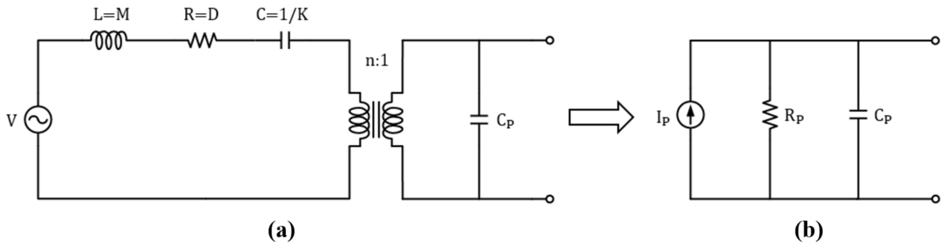
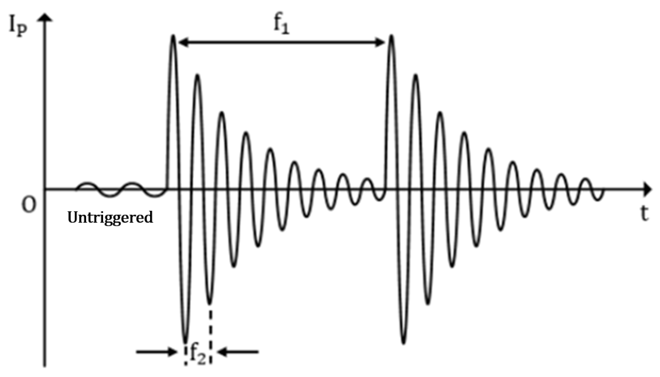
2. Output Energy Modeling
A piezoelectric energy harvester (PEH) is a device that converts vibration energy into electrical energy using piezoelectric materials, based on the principle of the piezoelectric effect. The classic architecture for PEHs is the cantilever beam structure, as depicted in Figure 1, which consists of a base, cantilever beam, mass block, and piezoelectric material [21]. The equivalent model of a cantilever beam PEH can be regarded as an electromechanical coupling model [22], illustrated in Figure 2a. In this model, voltage V represents the external vibration strength, inductance L represents the equivalent mass M, capacitance C represents the reciprocal of the mechanical stiffness K, resistance R represents the mechanical damping D, transformer n represents the electromechanical coupling coefficient, and capacitance represents the inherent capacitance of the piezoelectric material. When the PEH vibrates stably at its natural resonance frequency , the electromechanical coupling model shown in Figure 2a can be further simplified to the equivalent circuit shown in Figure 2b, which is a parallel circuit comprising a current source , a resistor , and a capacitor . The expressions for and are as follows:
Figure 1.
Structure of a cantilever beam PEH [23].
Figure 2.
(a) Equivalent electrical model of a cantilever beam PEH, (b) equivalent circuit of (a) at resonance [23,24].
Among these, the value of resistor is significantly higher than 1/, making its impact negligible in circuit design. In the open circuit state, the equivalent current source only loads the parasitic capacitance , thus the PEH’s open circuit voltage waveform resembles the current source ’s waveform, with a 90° phase shift. Figure 3 illustrates the open circuit voltage waveform of the PEH, where voltage represents its open circuit voltage and is its peak open circuit voltage.
Figure 3.
Open circuit voltage waveform of a cantilever beam PEH.
Given that the equivalent current source of a cantilever beam PEH maintains a stable sine wave during steady oscillation, with nearly constant frequency and amplitude, the cantilever beam PEH can be considered a constant excitation source for its energy extraction circuit.
With continuous advancements in manufacturing processes, PEHs are moving towards miniaturization. Shrinking device sizes have resulted in cantilever beam PEHs having higher resonant frequencies, reaching hundreds or even thousands of hertz. However, environmental vibrations typically occur at lower frequencies, mostly below 100 Hz, which substantially differ from the PEHs’ resonant frequencies, thereby reducing the power generation efficiency of cantilever beam PEHs. To address these shortcomings, this paper utilizes a two-stage vibration structure PEH with up-conversion functionality [25,26,27], as illustrated in Figure 4.
Figure 4.
Structure of a two-stage vibration structure PEH [26].
The energy harvester includes two stages of vibrators. The first stage is a U-shaped inductive vibrator with a mass block, designed to sense low-frequency environmental vibrations typically below 50 Hz. The second stage is a cantilever beam generating vibrator, with a natural resonance frequency usually above 100 Hz. At the corresponding ends of the inductive and generating vibrators, magnets are placed, arranged like poles facing each other to achieve magnetic coupling through repulsion.
This PEH uses magnetic coupling to realize “up-conversion”. When the environmental vibration intensity is weak, the inductive vibrator cannot overcome the magnetic repulsion between the magnets and can only perform minor vibrations around the equilibrium position, generating minimal electrical energy. As the vibration intensity increases, the vibration amplitudes of both vibrators grow. Once the vibration intensity surpasses a threshold, the inductive vibrator overcomes the magnetic repulsion, resulting in large vibration amplitudes and exciting the generating vibrator to oscillate at its natural resonance frequency, producing a substantial amount of electrical energy. This method significantly enhances power generation efficiency compared to cantilever beam PEHs.
Since the resonance frequency of the second-stage generating vibrator is much higher than the first-stage inductive vibrator’s vibration frequency, the generating vibrator in the cantilever beam structure experiences impulse excitation. Upon excitation, the generating vibrator performs damped oscillations at its natural resonance frequency, leading to an equivalent current source waveform, as shown in Figure 5. When the vibration intensity is below the threshold, the current is very weak. Once the intensity exceeds the threshold, the equivalent current source undergoes periodic damped oscillations. In Figure 5, two frequencies and are shown, representing the inductive stage vibration frequency (environmental vibration frequency) and the generating stage vibration frequency (generating stage’s natural resonance frequency), respectively, with . Similarly, the open circuit voltage waveform of the two-stage vibration structure PEH resembles the current source waveform, with a 90° phase difference.
Figure 5.
Equivalent current source waveform of the two-stage vibration structure PEH.
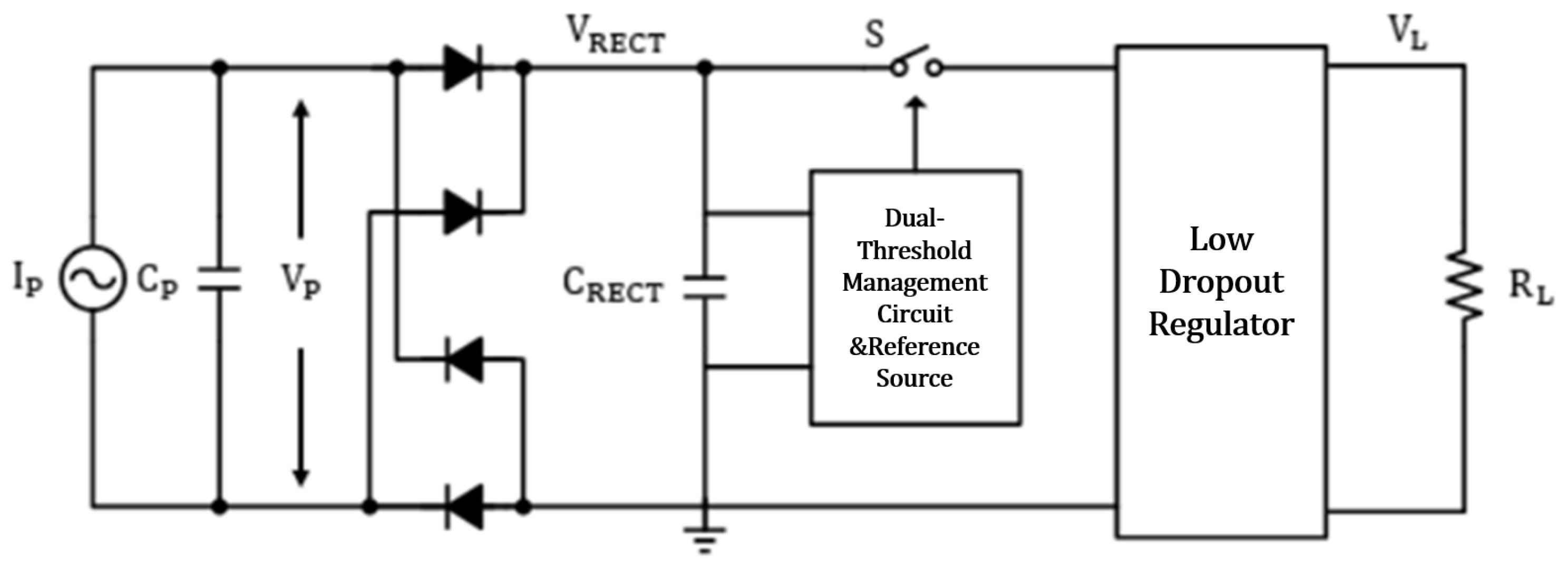
3. Circuit Implementation
Figure 6 illustrates the proposed architecture of the FBR and energy management circuit system. The PEH is represented as a parallel circuit of a current source and a capacitor . The rectifier bridge converts the AC output from the PEH into DC, and a storage capacitor stores the rectified electrical energy. The reference source supplies the reference voltage and current for the dual-threshold management circuit and the low dropout regulator (LDO). The dual-threshold management circuit monitors the voltage of the storage capacitor and activates a switch to transfer the stored energy to subsequent circuits once the capacitor’s voltage is sufficiently high. Since the storage capacitor’s voltage is unstable and cannot directly power the load, an LDO is placed between the load and the storage capacitor. The rectifier bridge, reference source, dual-threshold management circuit, and LDO are integrated on-chip, while the storage capacitor is an off-chip tantalum capacitor. Due to the PEH’s miniaturized design, its output power is only in the micro-watt range. Therefore, the circuit’s power consumption must be minimized before the switch is activated, during the storage capacitor’s charging process. In this design, both the reference source and the dual-threshold management circuit are optimized for ultra-low power consumption.
Figure 6.
Proposed full-bridge rectifier and energy management circuit system architecture.
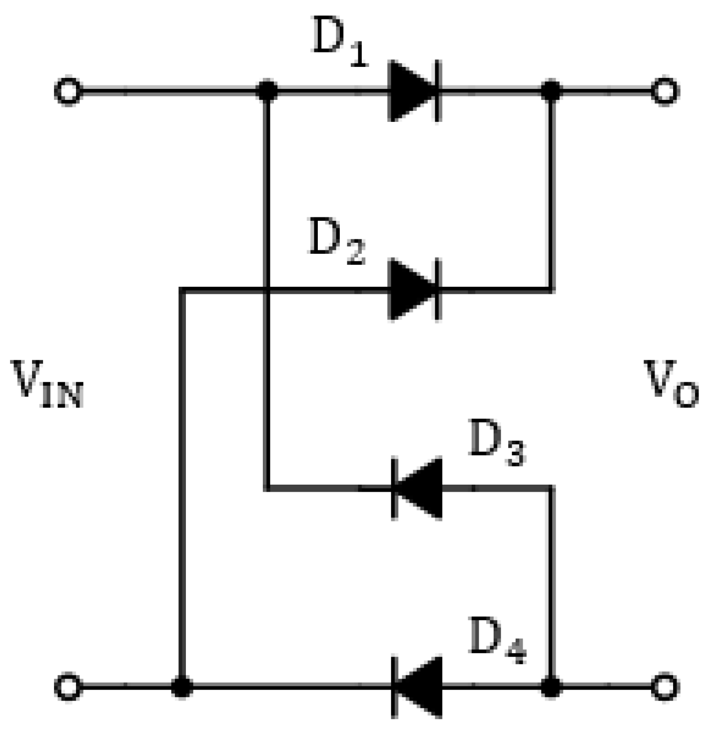
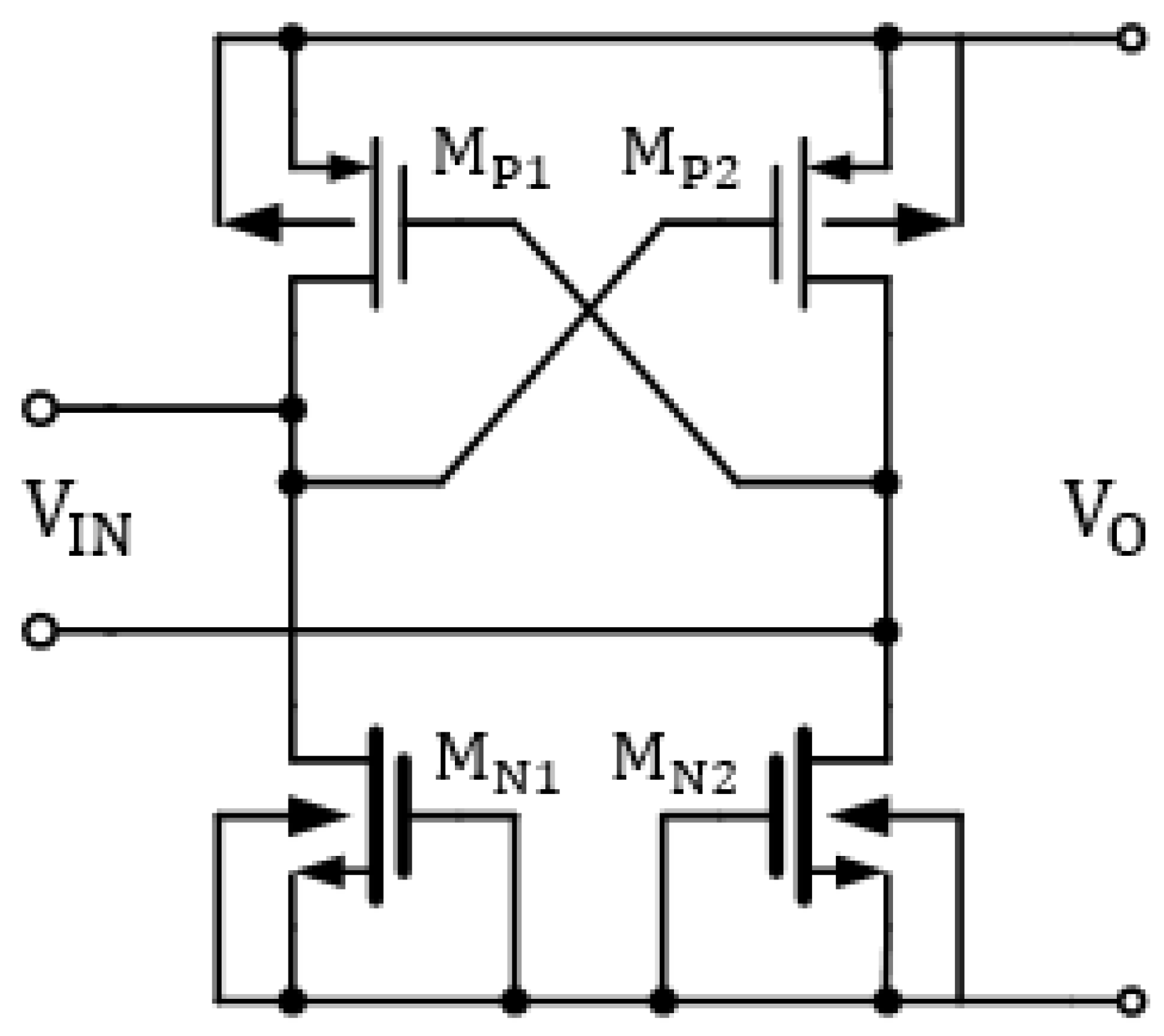
3.1. Cross-Coupled Rectifier Bridge Circuit
The output of the PEH is in AC form and cannot be directly stored in a storage capacitor, necessitating an interface circuit for AC–DC conversion. The diode FBR circuit is one common method to achieve this, as shown in Figure 7. This circuit consists of four diodes, each with a forward voltage drop of . When the input voltage is positive and exceeds 2, the circuit loop formed by diodes and conducts, allowing the output voltage to follow the input voltage . Conversely, when the input voltage is negative and below -2, the loop formed by diodes and conducts, with the output voltage inversely following the input voltage . Traditional rectifier bridges face two major drawbacks: firstly, when the input voltage , all input energy is wasted; secondly, when , the 2 forward voltage drop results in significant energy loss. Thus, traditional rectifier bridges are not ideal for PEH-based energy harvesting systems.
Figure 7.
Traditional rectifier bridge.
Transistor-based rectifier bridges, particularly cross-coupled designs, have become prevalent due to their low forward voltage drops. The rectifier bridge design in this work is shown in Figure 8 [28,29,30]. Transistors and are cross-coupled, while transistors and are diode-configured. Cross-coupled PMOS transistors operate in the deep linear region at higher input voltages, reducing the source-drain voltage drop significantly during conduction. The diode-connected NMOS transistors have a near-zero threshold voltage with a forward voltage drop around 200 mV, and they also prevent reverse current flow.
Figure 8.
Gate cross-coupled rectifier bridge.
The input-output simulation waveforms of the cross-coupled rectifier bridge are shown in Figure 9. The waveforms indicate that when mV, the rectifier bridge conducts, allowing the output voltage to follow the input voltage. After conduction, the voltage difference between input and output is less than 200 mV. Compared to traditional rectifier bridges, the cross-coupled design offers a lower turn-on voltage and reduced forward voltage drop.
Figure 9.
Simulation results of the proposed cross-coupled rectifier bridge.
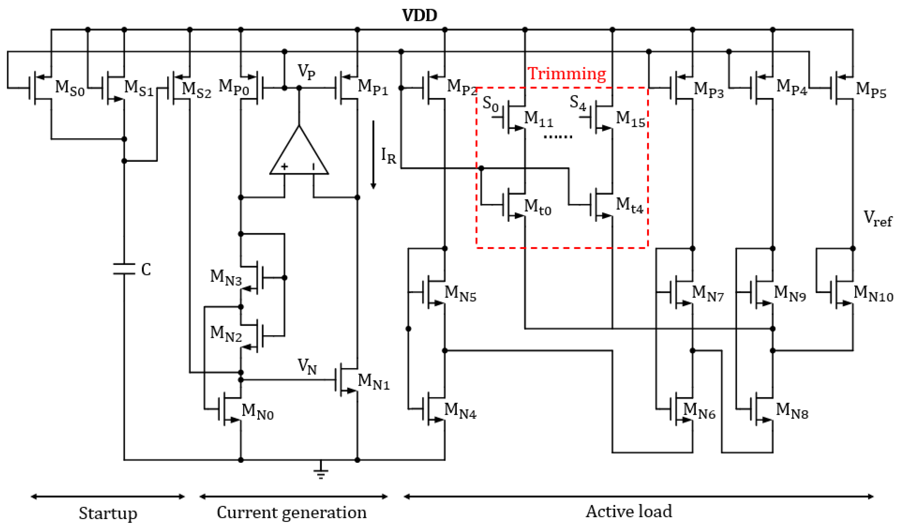
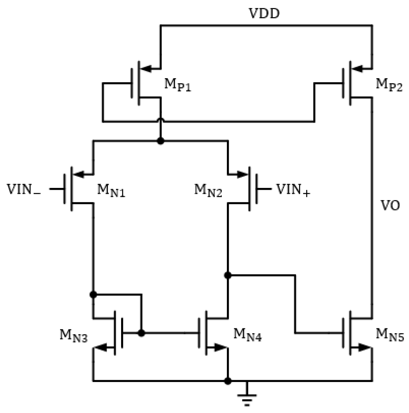
3.2. Reference Source Circuit
Given that all of the energy for the energy management chip is derived from the PEH, achieving optimal energy efficiency necessitates extremely low power consumption within the chip itself. The reference source, as a fundamental module in the energy management chip, provides the reference voltage and current for other circuit modules, thus determining the static power consumption of the entire chip [31,32,33,34]. The commonly used bandgap reference (BGR) based on BJTs has advantages such as low temperature coefficient, easy compensation, and stable performance. However, BGRs generally have high power consumption, and low-power BGR designs require large resistors and capacitors, which are unfavorable for integrated chip design. In this design, the traditional BJT-based BGR is replaced by a fully CMOS topology reference source. By leveraging sub-threshold transistor technology and the temperature characteristics of transistor threshold voltage, an ultra-low power reference circuit was developed, providing a reference current as low as 10∼20 nA, ensuring the ultra-low static power consumption of the energy management chip.
Figure 10 presents the fully CMOS low-power reference source used in this design [35], comprising a startup circuit, current generation circuit, active load circuit, and trimming circuit. The startup circuit includes transistors , , , and capacitor C. When is powered on, the voltage on C is zero, and the diode-connected transistor charges C. When the voltage on C has not yet risen to , transistor injects charge into node , initiating the circuit. After initiation, transistor turns on to charge C, accelerating its charging. Once C is charged to , the startup circuit shuts off, concluding the startup process. To ensure ample startup time, i.e., sufficient charging time for C, the size of transistor is set to 1 m/10 m.
Figure 10.
Fully CMOS low-power reference source [35].
The current generation circuit consists of transistors , , ∼, and an operational amplifier. Under the negative feedback of the operational amplifier, the drain voltages of transistors and are equal, thus the currents through both transistors are equal, each being . Transistor operates in the saturation region, in the linear region, and and in the sub-threshold region. The current–voltage relationship for a transistor in the sub-threshold region is expressed as
where is the sub-threshold slope factor, is the reverse saturation current, and = , = .
From Equation (5), the source-drain voltage difference of transistor is
where
Transistor operates in the linear region, thus it is equivalent to a resistor :
From Equations (6) and (7),
Solving Equations (8) and (9) simultaneously yields
where and .
The active load circuit includes transistors ∼, ∼. Transistors ∼ form a current mirror, replicating the current generated by the current generation circuit. Transistors ∼ operate in the sub-threshold region, thus the reference voltage is given by
where represents the transistor’s threshold voltage at 0 K, and varies under different process corners, with being the temperature coefficient.
Equation (11) shows that by adjusting the sizes of the transistors in the active load circuit, a nearly temperature-independent reference voltage can be obtained. However, due to process variations, transistors with the same dimensions can have slight differences in parameters such as , , and , and manufacturing inaccuracies can further affect transistor sizes. Therefore, a trimming circuit is necessary. As shown in Figure 10, by controlling the on/off states of transistors ∼, the total current through the active load circuit can be adjusted to fine-tune the temperature coefficient of the reference voltage. To minimize power consumption, all transistors in the reference source circuit operate in the sub-threshold region (except for and ).
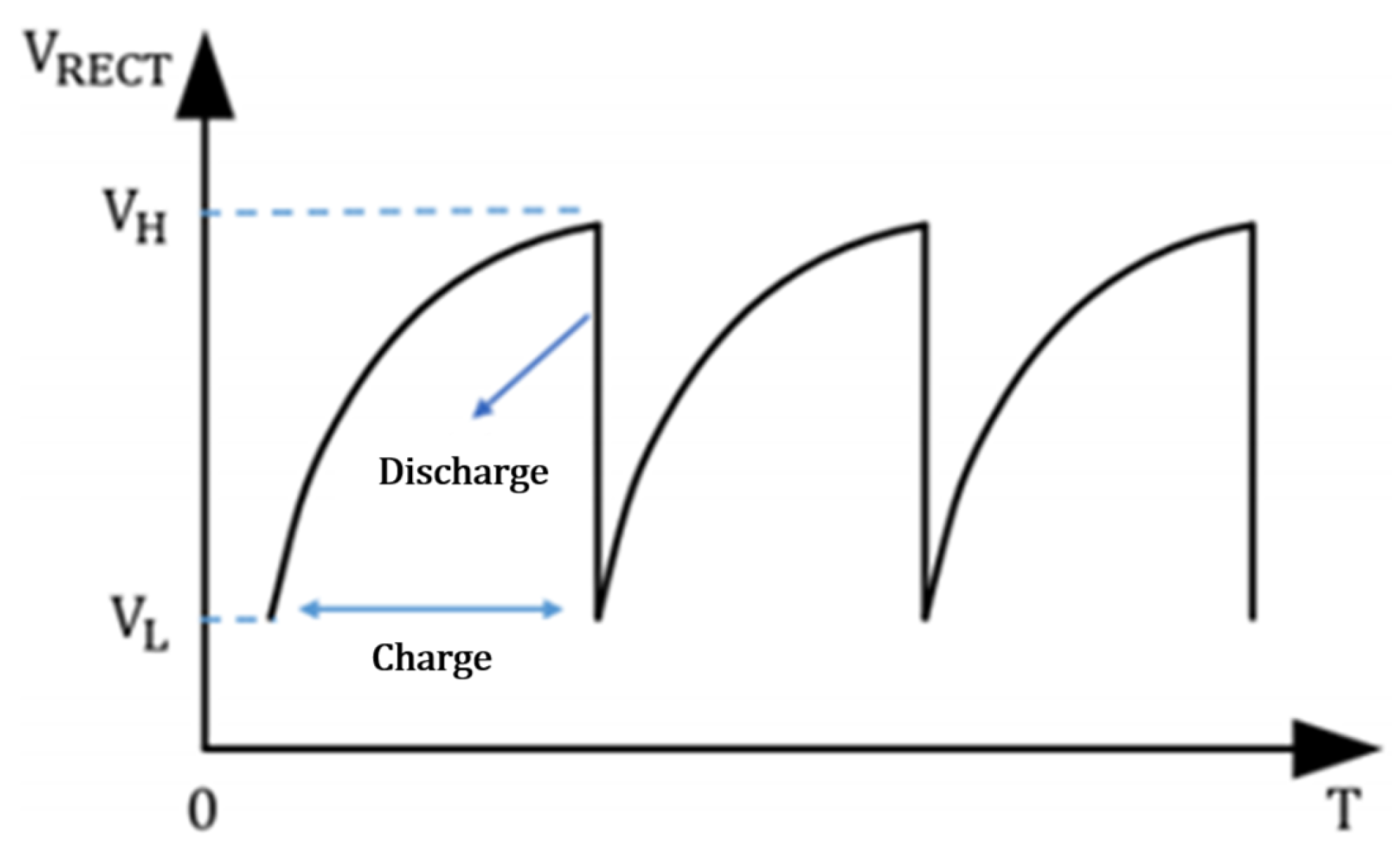
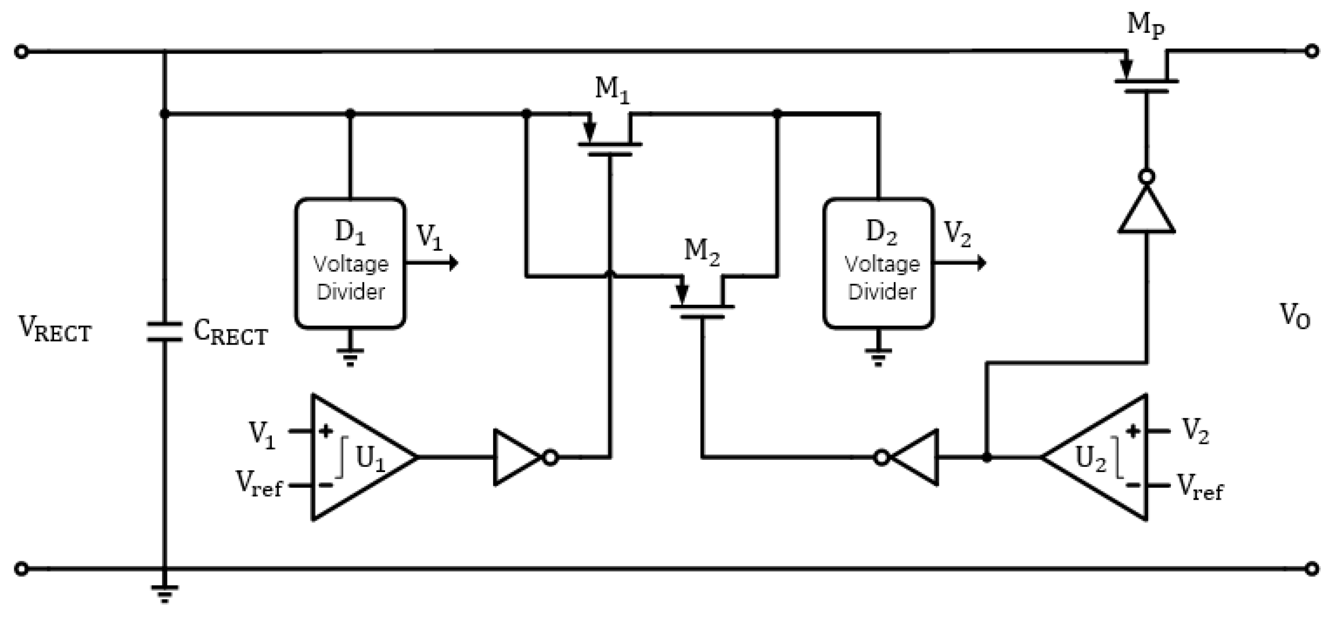
3.3. Energy Management Circuit
Wireless sensor nodes often include load modules such as power amplifiers and wireless transmitters, which typically require operating voltages between 2 V and 5 V and consume power in the milliwatt range, significantly higher than the output power of PEHs. Therefore, load modules cannot be directly connected to the storage capacitor; otherwise, they would drain the capacitor quickly and fail to operate properly. This requires the addition of an energy management circuit between the energy storage capacitor and the load module to achieve intermittent load driving. For stable load operation, the energy management circuit must ensure two functions: adequate energy storage in the capacitor to power the load for each operation cycle, and providing a stable voltage to the load.
The dual-threshold management circuit fulfills the first function, and it is used to detect the voltage across the energy storage capacitor and control its charging and discharging process. It has high () and low () thresholds, as shown in Figure 11. When the voltage on the storage capacitor is below the high threshold , switch S remains off, and the capacitor charges. Once reaches , S closes, allowing the capacitor to discharge rapidly. When the voltage drops to the low threshold , S opens again, returning the capacitor to the charging state. Compared to the classic LTC3588-1 dedicated energy harvesting chip, the dual threshold management circuit added in the proposed chip simplifies the circuit structure by setting appropriate high and low threshold voltages based on the energy consumption requirements of the load during operation, converting energy value detection into voltage value detection, and achieving this function under extremely low power consumption conditions. Efficient and reliable energy management can be achieved by controlling the charging and discharging of energy storage capacitors. In this design, the high threshold is set to 4.2 V and the low threshold to 2.2 V. The LDO then stabilizes the voltage, providing a consistent 1.8 V to the load post-discharge.
Figure 11.
Working process of the dual-threshold management circuit.
The proposed dual-threshold management circuit, shown in Figure 12, consists of a voltage divider circuit , , comparators , , and switching transistors , , and . The voltage divider circuit and generate voltages and , respectively, with . The switching transistor is a power transistor with dimensions of 2500 m/1 m, and its gate is controlled by , with its source-drain terminals connected to and the output. The comparators adopt a two-stage structure as shown in Figure 13. The first stage is a differential pair with a current mirror load, converting differential input to single-ended output. The second stage is a common-source amplifier with a current source load, providing large output swing and high gain. This structure is similar to a two-stage operational amplifier, but differs in that the comparator typically uses an open-loop configuration without compensation, resulting in high unity-gain bandwidth and response speed. Given the reference voltage value around 700 mV and the transistor operating voltage, PMOS transistors are chosen for the input pair. To meet power consumption requirements, the comparator’s bias current is provided by the reference source, with each branch current set to 20 nA, totaling 80 nA. The voltage divider circuit is implemented using resistors.
Figure 12.
Proposed dual-threshold management circuit.
Figure 13.
Proposed two-stage comparator.
Since the storage capacitor’s voltage is not constant and varies over time, a voltage regulation module is required to provide a stable and clean power supply to the load before delivering energy. The regulation module generally includes a switching power supply and an LDO. Compared to switching power supplies, LDOs offer lower output ripple and fewer external components, making them suitable for this system. The LDO circuit is shown in Figure 14, consisting of a folded cascode operational amplifier, a power transistor , and a resistor divider feedback loop. The LDO operates as a negative feedback loop, where the output voltage generates a feedback voltage through the resistor divider circuit. The feedback voltage is compared with the reference voltage in the folded cascode operational amplifier. The amplifier’s output controls the gate of the power transistor , thereby regulating the output voltage.
Figure 14.
Proposed LDO circuit.
Figure 15 shows the simulation waveform of the proposed energy management circuit. The voltage is set as a periodic signal, as shown by the red waveform in Figure 15, rising linearly from 2 V to 4.5 V within 0–2 s, and then falling linearly from 4.5 V to 2 V within 2–4 s. When is below 4.2 V, the voltage generated by the voltage divider circuit is lower than , causing comparator to output a low level, turning off the switching transistor . The voltage generated by the voltage divider circuit is zero, causing comparator to output a low level, turning off the switching transistor and the power transistor . When rises above 4.2 V, exceeds , causing to output a high level, turning on the switching transistor . The also exceeds , causing to output a high level, turning on the switching transistor and , and the LDO outputs a voltage of 1.8 V. When drops below 2.2 V, both and are lower than , causing and to output low levels, turning off the switching transistors , , and the power transistor , resulting in zero LDO output voltage.
Figure 15.
Simulation waveform of the proposed energy management circuit.
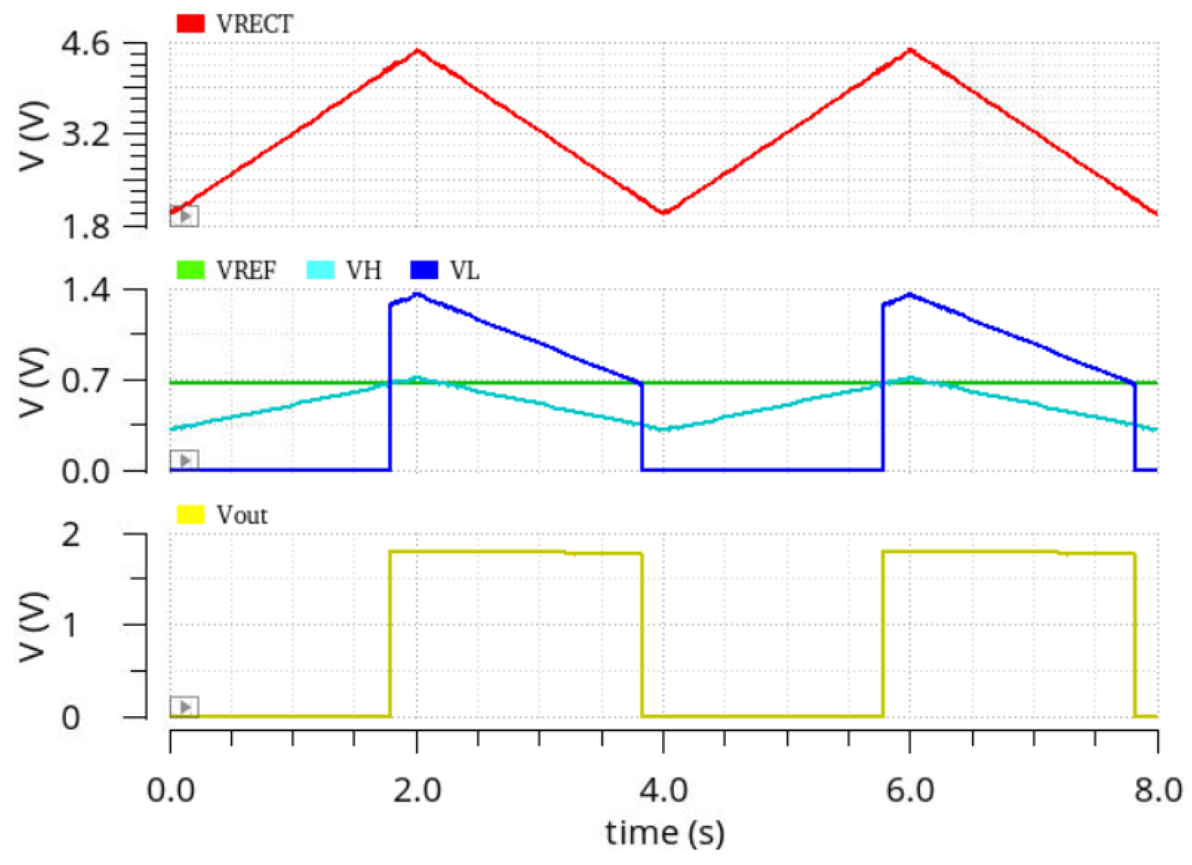
3.4. System-Level Simulation
The individual circuit modules were integrated into an overall system and simulated using the Cadence Spectre simulation tool. Currently, the parasitic capacitance values of miniaturized PEHs are mostly below 50 nF. Therefore, the parasitic capacitance was set to 20 nF for the simulation. Considering the two-stage vibration structure of the PEH, the first-stage inductive vibrator senses environmental vibrations with a frequency matching the environmental vibration frequency, while the second-stage generating vibrator operates at its natural resonance frequency . The equivalent current source characteristics are as analyzed in Section 2. For the simulation, was set to 40 Hz, to 400 Hz, and the peak value of the vibrating current source was set to 300 A. The waveform is shown as the red waveform in Figure 16. In addition to setting PEH parameters, the off-chip storage capacitor was set to 100 F, and the load resistor was set to 600 Ω.
Figure 16.
PEH output characteristics simulation under the FBR interface circuit.
The system’s operational state was simulated and analyzed, including the PEH output characteristics, the voltage of the storage capacitor, and the load voltage . Figure 16 shows the PEH output characteristics simulation waveform under the FBR interface circuit. Figure 17 shows the enlarged view of the simulation waveform in Figure 16, including the equivalent current source , the current flowing into the storage capacitor, and the voltage .
Figure 17.
Enlarged view of the simulation waveform in Figure 16.
From Figure 16 and Figure 17, it can be observed that when the FBR interface circuit is in operation, a considerable portion of the current generated by the equivalent current source is used for charging and discharging the parasitic capacitance to turn on the rectifier bridge, with only a part of the current flowing into the storage capacitor. As the voltage on the storage capacitor increases, the voltage required to turn on the rectifier bridge also increases, leading to even higher energy losses due to charging and discharging . When decays to a sufficiently low level, all its current is used for charging and discharging the parasitic capacitance, with no current flowing into the storage capacitor.
Figure 18 shows the waveforms of the storage capacitor voltage and the load voltage in the system-level simulation. The on the storage capacitor starts rising from 0, and when it reaches the high threshold of 4.2 V, the storage capacitor begins to discharge, providing a regulated 1.8 V to the load through the LDO. When the storage capacitor voltage drops to the low threshold of 2.2 V, the storage capacitor stops discharging, and the load voltage drops to 0. The load operates intermittently, with an operation cycle of approximately 5.82 s. From the previous analysis, it is clear that the system can effectively achieve both energy harvesting and power management.
Figure 18.
System simulation waveform of the storage capacitor voltage and load voltage .
In addition to analyzing the system’s operational state, it is essential to evaluate the energy extraction power. During normal operation, the peak voltage of the PEH output voltage varies, making it impossible for the FBR interface circuit to determine a maximum power point. Therefore, the energy extraction power of the FBR interface circuit is represented by the average energy obtained by the storage capacitor between the high and low voltage thresholds,
where is the load’s intermittent operation period.
From the simulation, the average output power of the PEH over the period is
Thus, the energy transmission efficiency of the FBR interface circuit is approximately 92.4%.
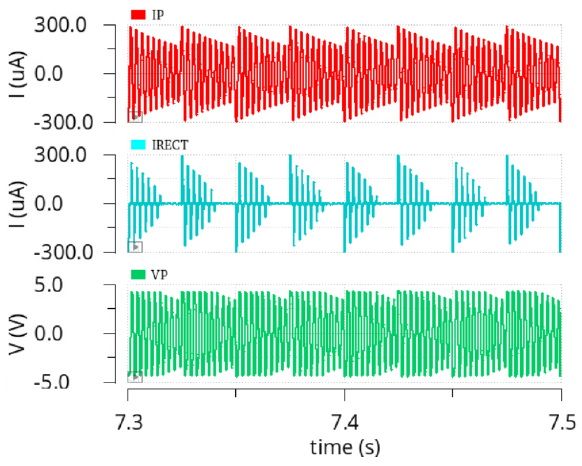
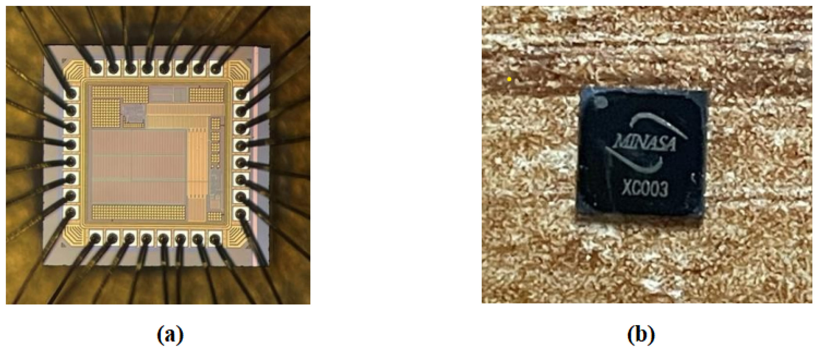
4. Measurement Results
The circuit was designed using a 110 nm CMOS process. Figure 19a shows the chip under a microscope, and Figure 19b shows the chip packaged in a QFN32 package, with the packaged chip size being 4 × 4 mm2. The size of the piezoelectric energy harvester is much larger than the designed energy harvesting and management chip, so it can only be soldered on a PCB board for testing and cannot be integrated together.
Figure 19.
(a) Microscopic view of the chip’s bonding wires. (b) Energy harvesting and management chip in QFN32 package.
The physical image of the piezoelectric vibration energy harvester used in this experiment is shown in Figure 20. It is packaged in an organic glass tube shell with copper foil leading out the electrode. The size of the packaged device is 21.0 × 14.0 × 11.0 mm3. When it is actually applied in wireless monitoring sensing systems, the fixed outer frame required for packaging needs to be removed, and the core structural area is only 17.0 × 8.0 mm2. The size and material parameters of the device are shown in Table 1.
Figure 20.
Physical picture of piezoelectric vibration energy harvester.
Table 1.
Dimensions and material parameters of piezoelectric vibration energy harvester.
In this test, the storage capacitor value was 100 F, the load current was set to 3 mA, i.e., the load resistance was 600 Ω, the vibration frequency of the shaker was set to 40 Hz, and the vibration acceleration was set to 4 g. Figure 21a shows the measured waveforms of the storage capacitor voltage and the load voltage . Figure 21b shows an enlarged view of the waveforms in Figure 21a. The measured waveforms indicate that the chip’s operation is consistent with the simulation, demonstrating the ability to perform piezoelectric energy harvesting and power management. The storage capacitor switches between charging and discharging states, with the dual-threshold management circuit effectively detecting voltage changes on the storage capacitor and controlling its discharge. The measured high threshold is approximately 4.4 V, and the low threshold is approximately 2.3 V. The LDO provides a stable output voltage of 1.8 V during the storage capacitor discharge. The load operates intermittently, with an operation cycle of approximately 3 s. Therefore, under the above test conditions, the chip’s energy extraction power is approximately 234 W.
Figure 21.
(a) Measured waveforms of the chip. (b) Enlarged view of the measured waveforms.
According to the actual test results, the high and low thresholds of the dual threshold management circuit are slightly different from those in the simulation, and it is speculated that there are two reasons for this. Firstly, there are process errors in actual film production. The voltage divider circuit is composed of multiple identical resistors connected in series. In actual chip fabrication, due to process errors, there may be differences in the resistance values of multiple resistors, resulting in slight differences between the high and low thresholds in actual testing and simulation. Secondly, chip packaging brings parasitic parameters that affect chip operation, resulting in slight differences between high and low thresholds and simulation. Although the high and low thresholds of the dual threshold management circuit differ slightly from those in simulation, the difference is small and within the expected error range, it does not affect the normal operation of the chip.
Table 2 compares the performance of the FBR interface circuit designed in this work with that in other references. It can be seen from the comparison that the FBR interface circuit designed in this work has a higher energy extraction power and lower power consumption.
Table 2.
Performance summary and comparison.
5. Conclusions
This paper presents the system design of an FBR and energy management circuit, including a rectifier bridge, a fully CMOS reference source, and an energy management circuit. The rectifier bridge employs a PMOS cross-coupled structure to reduce the conduction voltage drop, thereby minimizing energy transmission losses. The traditional BJT-based BGR is abandoned in favor of a fully CMOS topology reference source in this design. Utilizing sub-threshold transistor technology and the temperature characteristics of transistor threshold voltage, an ultra-low power reference circuit is achieved, ensuring ultra-low static power consumption for the energy management chip. The dual-threshold energy management circuit converts energy value detection into voltage detection through the proper setting of high and low thresholds, significantly simplifying the circuit structure and achieving this function under ultra-low power conditions. The circuit is fabricated using a 110 nm CMOS process. Measurement results show that under a vibration frequency of 40 Hz and a vibration acceleration amplitude of 4 g, the chip’s energy extraction power is 234 W, and the load operates every 3 s with a stable power supply voltage of 1.8 V during operation. Therefore, this FBR interface circuit can effectively extract electrical energy from the PEH output.
Author Contributions
Conceptualization, S.L. and W.G.; methodology, S.C.; software, J.Z.; validation, W.G., J.Z. and X.Y.; formal analysis, Z.L.; investigation, D.X.; resources, D.X.; data curation, F.C.; writing—original draft preparation, S.L.; writing—review and editing, Z.L.; supervision, Z.L.; project administration, D.X. All authors have read and agreed to the published version of the manuscript.
Funding
This research was supported by the National Key Research and Development Program of China under Grant 2022YFB3205003.
Institutional Review Board Statement
Not applicable.
Informed Consent Statement
Not applicable.
Data Availability Statement
Data are contained within the article.
Conflicts of Interest
The authors declare no conflicts of interest.
Abbreviations
The following abbreviations are used in this manuscript:
| FBR | Full-Bridge Rectifier |
| PEH | Piezoelectric Energy Harvester |
| LDO | Low Dropout Regulator |
| BGR | Bandgap Reference |
References
- Agarkhed, J.; Ankalgi, R. Energy efficient smart home monitoring system in wireless sensor network. In Proceedings of the Power and Computing Technologies (ICCPCT), 2016 International Conference on Circuit, Nagercoil, India, 18–19 March 2016; pp. 1–7. [Google Scholar]
- Ruiz-Garcia, L.; Lunadei, L.; Barreiro, P.; Robla, J.I. A Review of Wireless Sensor Technologies and Applications in Agriculture and Food Industry: State of the Art and Current Trends. Sensors 2009, 9, 4728–4750. [Google Scholar] [CrossRef] [PubMed]
- Oudenhoven, J.F.M.; Vullers, R.J.M.; Schaijk, R.V. A review of the present situation and future developments of micro-batteries for wireless autonomous sensor systems. Int. J. Energy Res. 2012, 36, 1139–1150. [Google Scholar] [CrossRef]
- Akyildiz, I.F.; Su, W.; Sankarasubramaniam, Y. Wireless sensor networks: A survey. Comput. Netw. 2002, 38, 393–422. [Google Scholar] [CrossRef]
- Fernández-Lozano, J.J.; Martín-Guzmán, M.; Martín-Ávila, J.; García-Cerezo, A. A wireless sensor network for urban traffic characterization and trend monitoring. Sensors 2015, 15, 26143–26169. [Google Scholar] [CrossRef] [PubMed]
- Ulukus, S.; Yener, A.; Erkip, E.; Simeone, O.; Zorzi, M.; Grover, P.; Huang, K. Energy harvesting wireless communications: A review of recent advances. IEEE J. Sel. Areas Commun. 2015, 33, 360–381. [Google Scholar] [CrossRef]
- Shaikh, F.K.; Zeadally, S. Energy harvesting in wireless sensor networks: A comprehensive review. Renew. Sustain. Energy Rev. 2016, 55, 1041–1054. [Google Scholar] [CrossRef]
- Roundy, S.; Steingart, D.; Frechette, L.; Wright, P.; Rabaey, J. Power sources for wireless sensor networks. In Proceedings of the European Workshop on Wireless Sensor Networks, Berlin, Germany, 19–21 January 2004; pp. 1–17. [Google Scholar]
- Sue, C.Y.; Tsai, N.C. Human powered MEMS-based energy harvest devices. Appl. Energy 2012, 93, 390–403. [Google Scholar] [CrossRef]
- Xi, Y.; Guo, H.; Zi, Y.; Li, X.; Wang, J.; Deng, J.; Li, S.; Hu, C.; Cao, X.; Wang, Z.L. Multifunctional TENG for Blue Energy Scavenging and Self-Powered Wind-Speed Sensor. Adv. Energy Mater. 2017, 7, 1602397.1–1602397.6. [Google Scholar] [CrossRef]
- Paradiso, J.A.; Starner, T. Energy scavenging for mobile and wireless electronics. IEEE Pervasive Comput. 2008, 4, 18–27. [Google Scholar] [CrossRef]
- Lin, Y.; Wu, T.; Zeng, Y.; Yang, J.; Chen, W.; Li, Z. A 15 mV-input and 71%-efficiency boost converter with 22 mV output ripple for thermoelectric energy harvesting application. Microelectron. J. 2022, 121, 105353. [Google Scholar] [CrossRef]
- Harb, A. Energy harvesting: State-of-the-art. Renew. Energy 2011, 36, 2641–2654. [Google Scholar] [CrossRef]
- Beeby, S.P.; Tudor, M.J.; White, N.M. Energy harvesting vibration sources for microsystems applications. Meas. Sci. Technol. 2006, 17, 175–195. [Google Scholar] [CrossRef]
- Wang, H.; Jasim, A.; Chen, X. Energy harvesting technologies in roadway and bridge for different applications—A comprehensive review. Appl. Energy 2018, 212, 1083–1094. [Google Scholar] [CrossRef]
- Jin, Y.K.; Sarker, S.; Lee, K.S.; Seo, H.W.; Kim, D.M. Piezoelectric materials for high performance energy harvesting devices. In Proceedings of the Pan Pacific Microelectronics Symposium, Big Island, HI, USA, 25–28 January 2016; pp. 1–4. [Google Scholar]
- Oh, T.; Islam, S.K.; Mahfouz, M.; To, G. A Low-Power CMOS Piezoelectric Transducer Based Energy Harvesting Circuit for Wearable Sensors for Medical Applications. J. Low Power Electron. Appl. 2017, 7, 33. [Google Scholar] [CrossRef]
- Agorastou, Z.; Kalenteridis, V.; Siskos, S. A 1.02 µW Autarkic Threshold-Based Sensing and Energy Harvesting Interface Using a Single Piezoelectric Element. J. Low Power Electr. Appl. 2021, 27, 33. [Google Scholar]
- Lee, T.Z.; Liu, Y.-W. High efficiency active rectifier with low-power self-biased comparator for low-frequency piezoelectric vibration energy harvesting of AUV. Microelectron. J. 2024, 146, 156–167. [Google Scholar] [CrossRef]
- Shen, J.; Xia, Y.; Xia, H. ReL-SSHI rectifier based piezoelectric energy harvesting circuit with MPPT control technique. Microelectron. J. 2022, 121, 141–144. [Google Scholar] [CrossRef]
- Erturk, A.; Inman, D.J. A Distributed Parameter Electromechanical Model for Cantilevered Piezoelectric Energy Harvesters. J. Vib. Acoust. 2008, 130, 1257–1261. [Google Scholar] [CrossRef]
- Elvin, N.G.; Elvin, A.A. A General Equivalent Circuit Model for Piezoelectric Generators. J. Intell. Mater. Syst. Struct. 2009, 20, 3–9. [Google Scholar] [CrossRef]
- Roundy, S.; Wright, P.K. A piezoelectric vibration based generator for wireless electronics. Smart Mater. Struct. 2004, 13, 1131–1142. [Google Scholar] [CrossRef]
- Renaud, M.; Karakaya, K.; Sterken, T.; Fiorini, P.; Hoof, C.V.; Puers, R. Fabrication, modeling and characterization of MEMS piezoelectric vibration harvesters. Sens. Actuators A Phys. 2008, 145–146, 380–386. [Google Scholar] [CrossRef]
- Edwards, B.; Xie, M.; Aw, K.C.; Hu, A.P.; Gao, W. An impact based frequency up-conversion mechanism for low frequency vibration energy harvesting. In Proceedings of the Transducers and Eurosensors, Barcelona, Spain, 16–20 June 2013; pp. 1344–1347. [Google Scholar]
- Tang, Q. Micro-Energy Harvester Based on Coupling of Two-Stage Vibrational Structures; Microelectronics and Solid-State Electronics; University of Chinese Academy of Sciences: Beijing, China, 2015. [Google Scholar]
- Liu, J. Research on High-Efficiency Energy Capture of Piezoelectric Energy Harvesters and Technologies for Self-Powered Wireless Sensor Nodes; Soochow University: Suzhou, China, 2020. [Google Scholar]
- Niu, D.; Huang, Z.; Jiang, M.; Inoue, Y. A Sub-O.3 V CMOS Rectifier for Energy Harvesting Applications. In Proceedings of the IEEE 54th International Midwest Symposium on Circuits and Systems, Seoul, Republic of Korea, 7–10 August 2011. [Google Scholar]
- Belal, E.; Mostafa, H.; Said, M.S. Comparison between Active AC-DC Converters For Low Power Energy Harvesting Systems. In Proceedings of the 27th International Conference on Microelectronics, Casablanca, Morocco, 20–23 December 2015. [Google Scholar]
- Yeo, K.H.; Ali, S.H.M.; Menon, P.S.; Islam, M.S. Comparison of CMOS Rectifiers for Micropower Energy Harvesters. In Proceedings of the IEEE Conference on Energy Conversion (CENCON), Johor Bahru, Malaysia, 19–20 October 2015. [Google Scholar]
- Navidi, M.M.; Graham, D.W. A Low-Power Voltage Reference Cell with a 1.5 V Output. J. Low Power Electron. Appl. 2018, 8, 19. [Google Scholar] [CrossRef]
- Wang, S.; Lu, Z.; Xu, K.; Dai, H.; Wu, Z.; Yu, X. A Sub-1-V Nanopower MOS-Only Voltage Reference. J. Low Power Electron. Appl. 2023, 14, 13. [Google Scholar] [CrossRef]
- Rezaei, N.; Mirhassani, M. Ultra low-power negative DC voltage generator based on a proposed level shifter and voltage reference. Microelectron. J. 2021, 113, 155–159. [Google Scholar] [CrossRef]
- Zeng, Y.; Huang, Y.; Luo, Y.; Tan, H.Z. An ultra-low-power CMOS voltage reference generator based on body bias technique. Microelectron. J. 2013, 44, 1145–1153. [Google Scholar] [CrossRef]
- Parisi, A.; Finocchiaro, A.; Papotto, G.; Palmisano, G. Nano-power CMOS voltage reference for RF-powered systems. IEEE Trans. Circ. Syst. II Express Briefs 2018, 65, 1425–1429. [Google Scholar] [CrossRef]
- Ramadass, Y.K.; Chandrakasan, A.P. An Efficient Piezoelectric Energy Harvesting Interface Circuit Using a Bias-Flip Rectifier and Shared Inductor. IEEE J. Solid-State Circuits 2010, 45, 189–204. [Google Scholar] [CrossRef]
- Wu, L.; Do, X.-D.; Lee, S.-G.; Ha, D.S. A Self-Powered and Optimal SSHI Circuit Integrated with an Active Rectifier for Piezoelectric Energy Harvesting. IEEE Trans. Circuits Syst. I Regul. Pap. 2017, 64, 537–549. [Google Scholar] [CrossRef]
- Du, S.; Seshia, A.A. An Inductorless Bias-Flip Rectifier for Piezoelectric Energy Harvesting. IEEE J. Solid-State Circuits 2017, 52, 2746–2757. [Google Scholar] [CrossRef]
Disclaimer/Publisher’s Note: The statements, opinions and data contained in all publications are solely those of the individual author(s) and contributor(s) and not of MDPI and/or the editor(s). MDPI and/or the editor(s) disclaim responsibility for any injury to people or property resulting from any ideas, methods, instructions or products referred to in the content. |
© 2024 by the authors. Licensee MDPI, Basel, Switzerland. This article is an open access article distributed under the terms and conditions of the Creative Commons Attribution (CC BY) license (https://creativecommons.org/licenses/by/4.0/).