
PANDA: Processing in Magnetic Random-Access Memory-Accelerated de Bruijn Graph-Based DNA Assembly


Abstract
1. Introduction
2. PANDA Platform
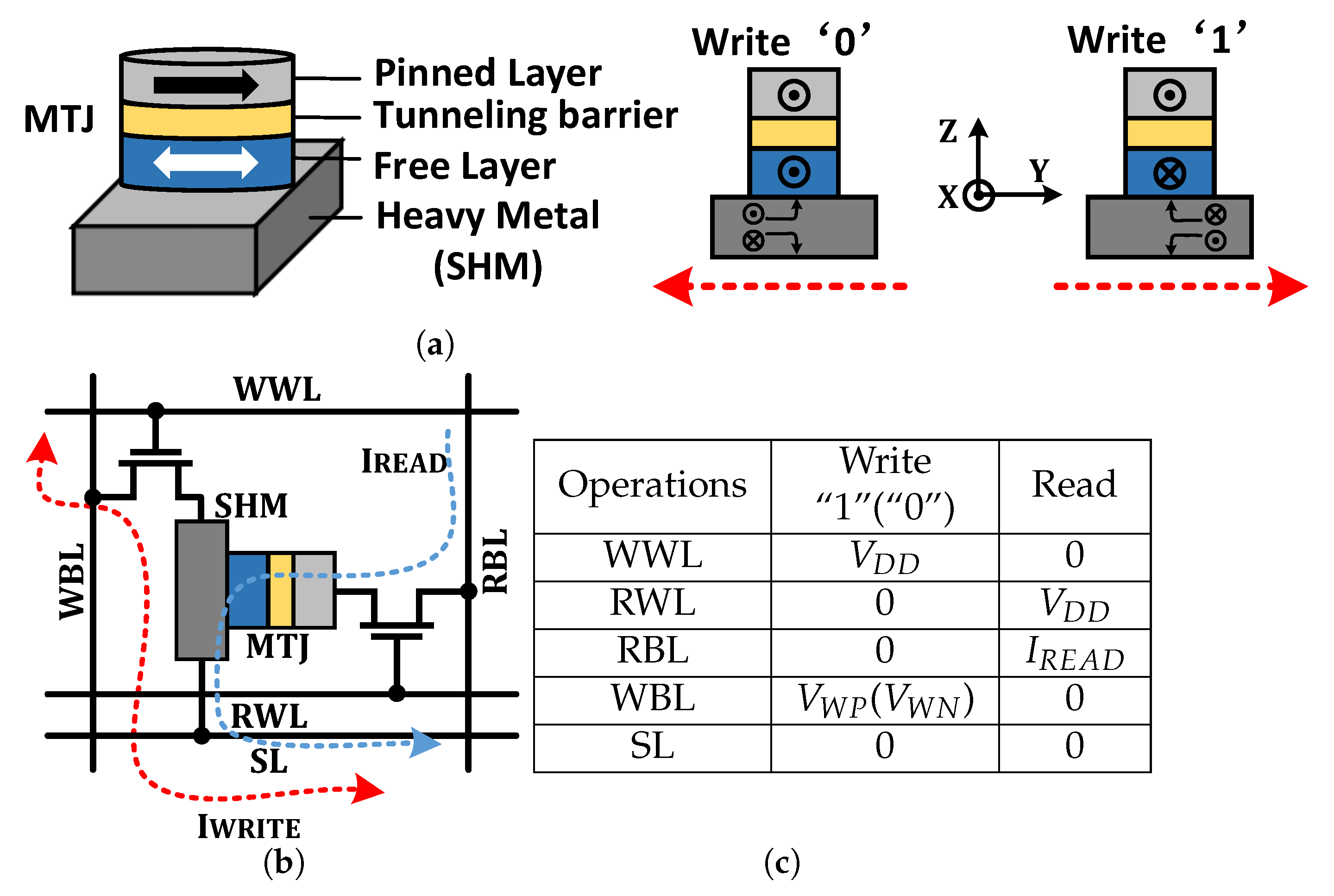
2.1. SOT-MRAM
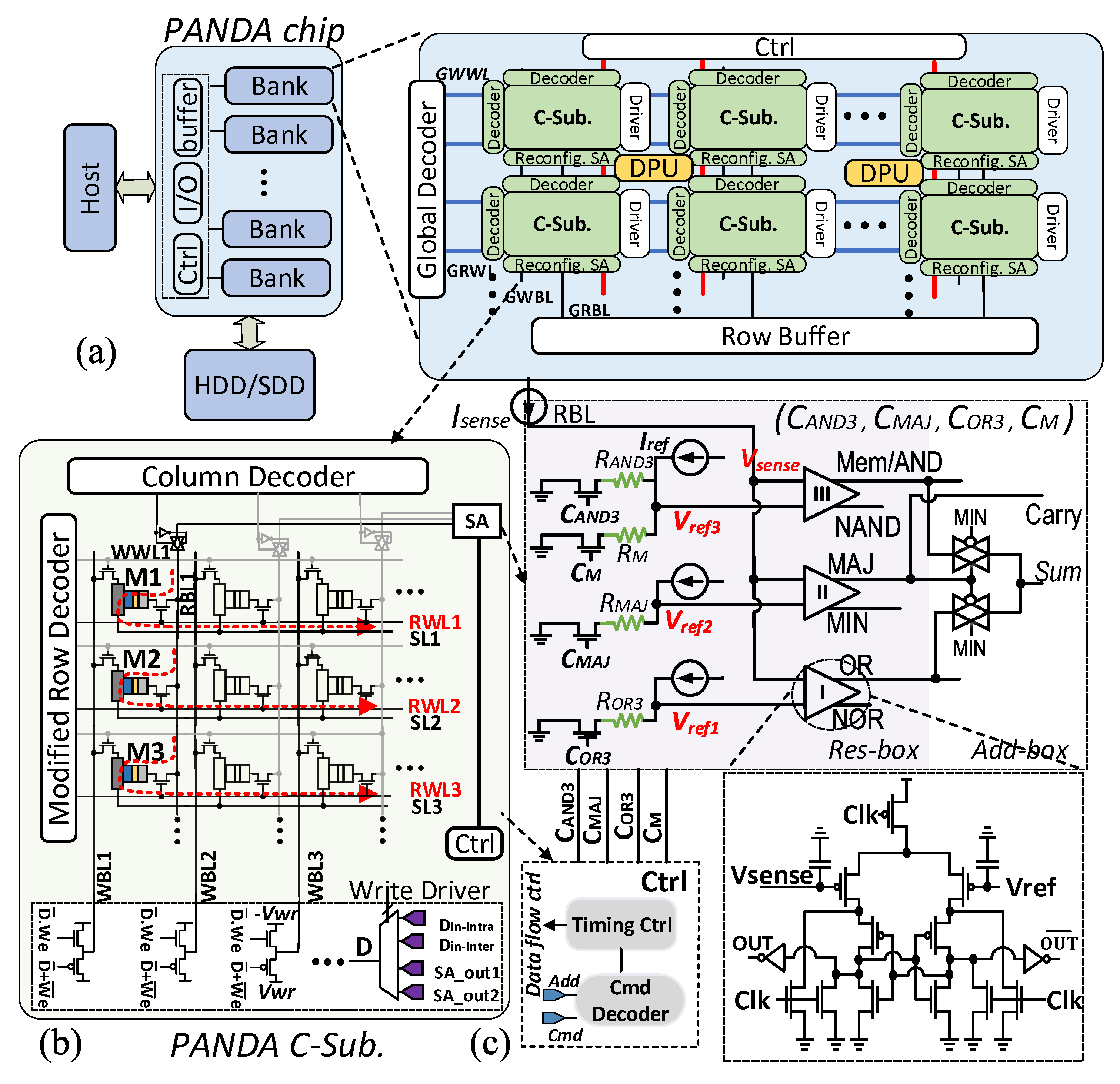
2.2. Architecture Design
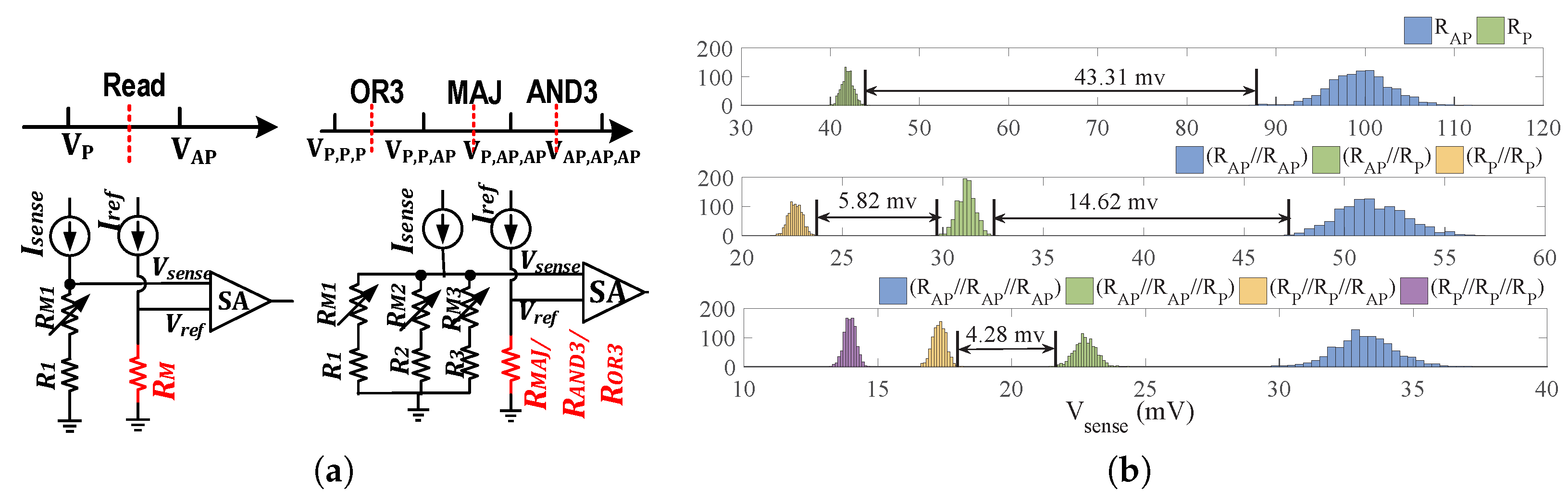
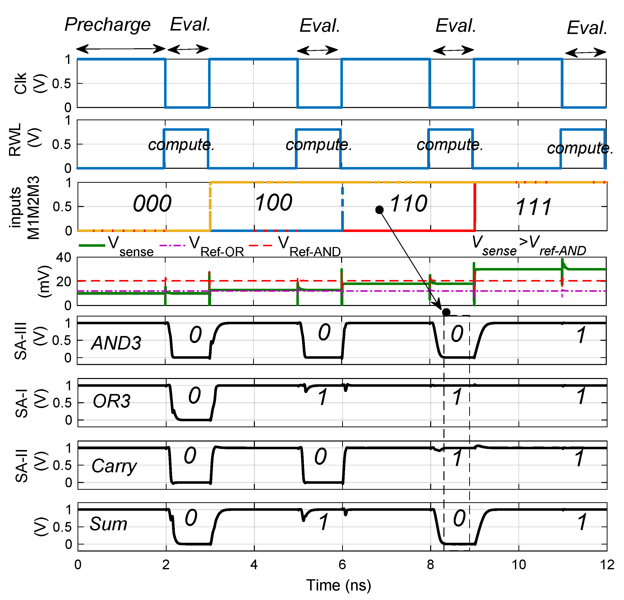
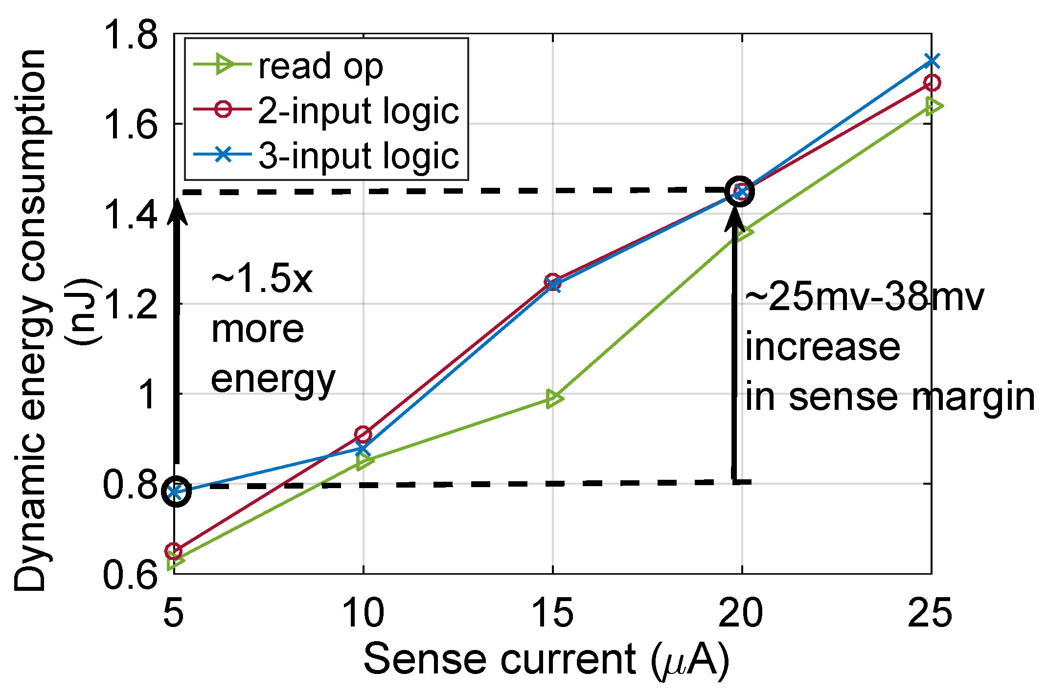
2.3. PIM Operations
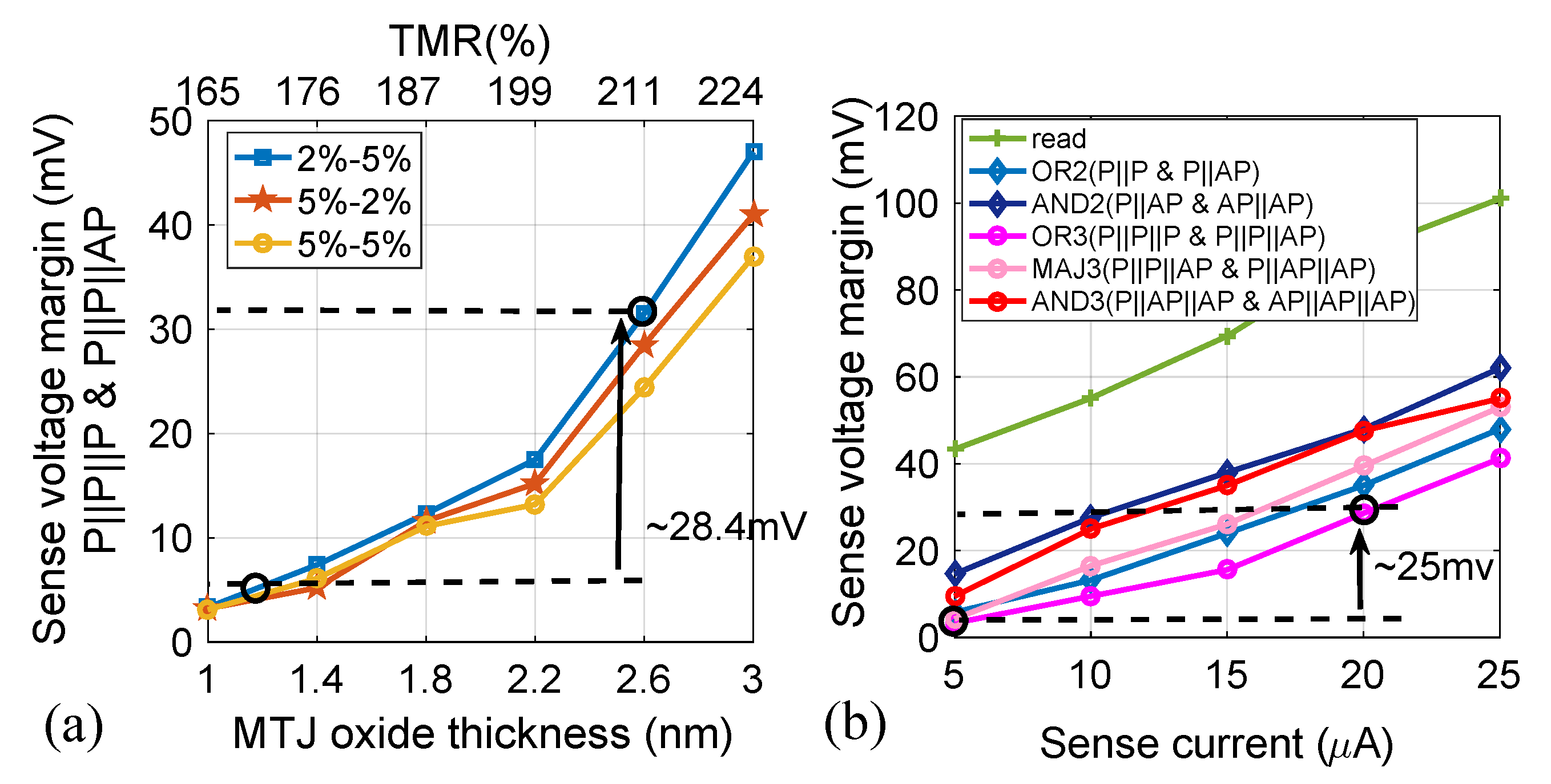
2.4. Performance Analysis
2.5. Software Support
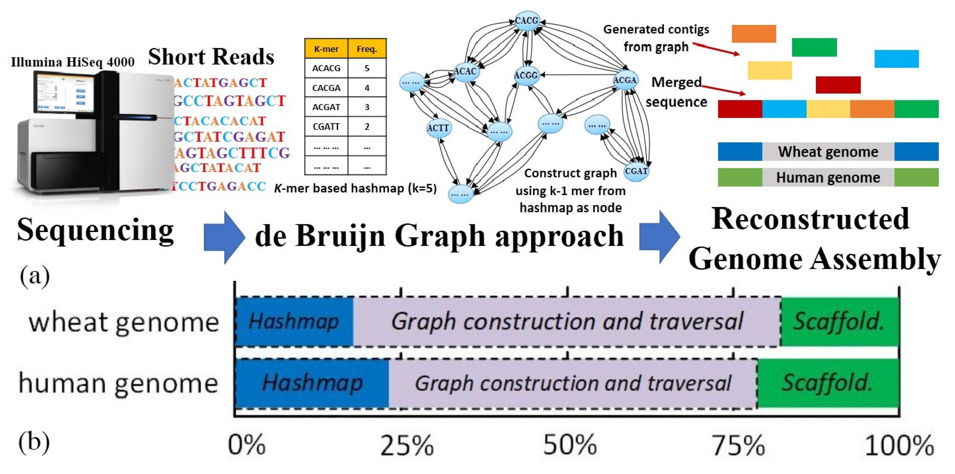
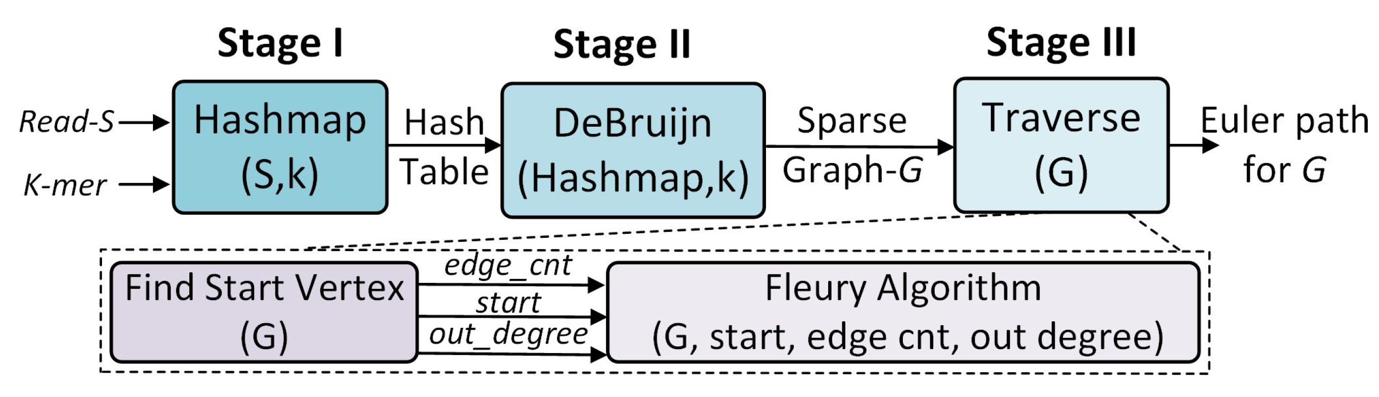
3. PANDA Algorithm and Mapping
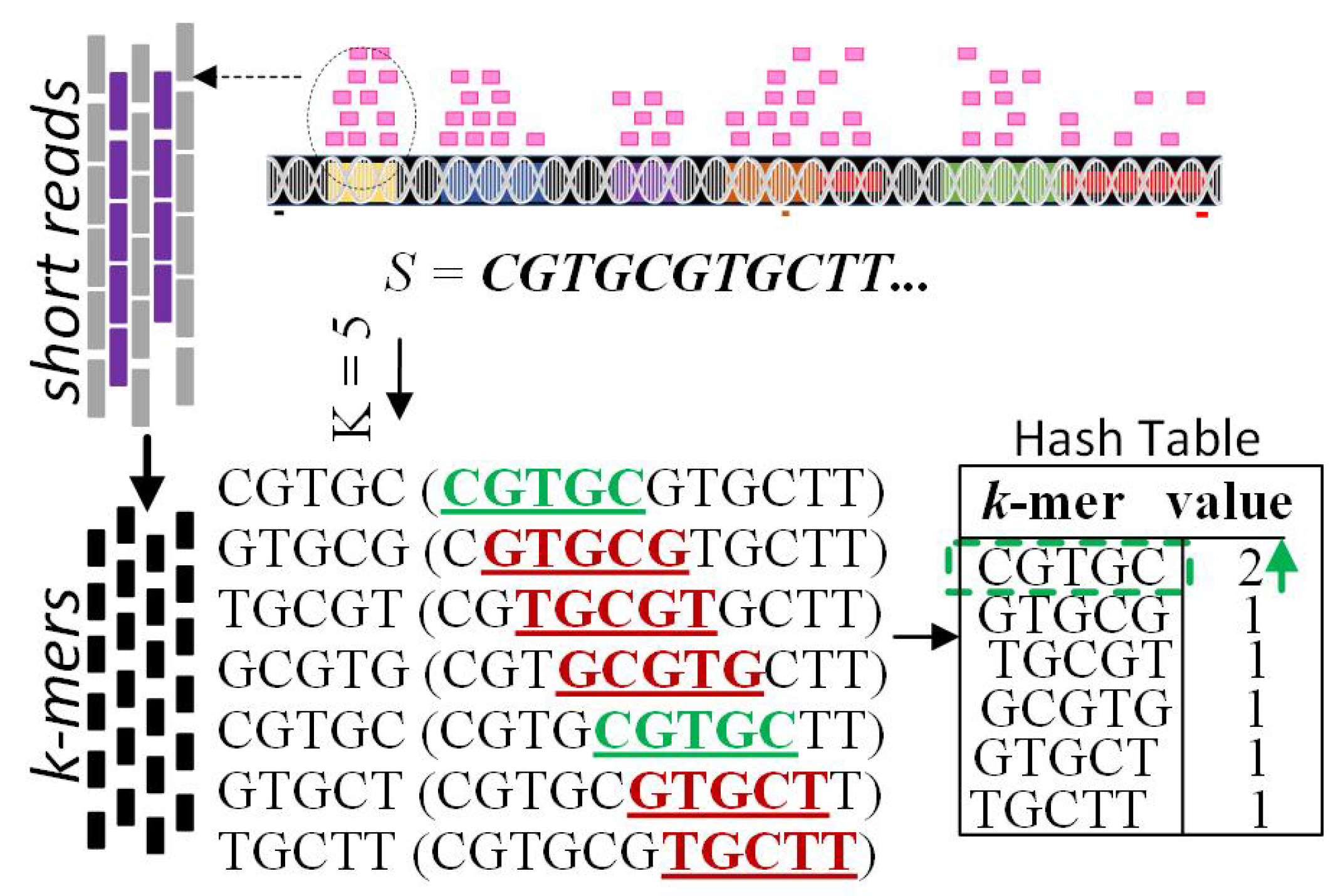
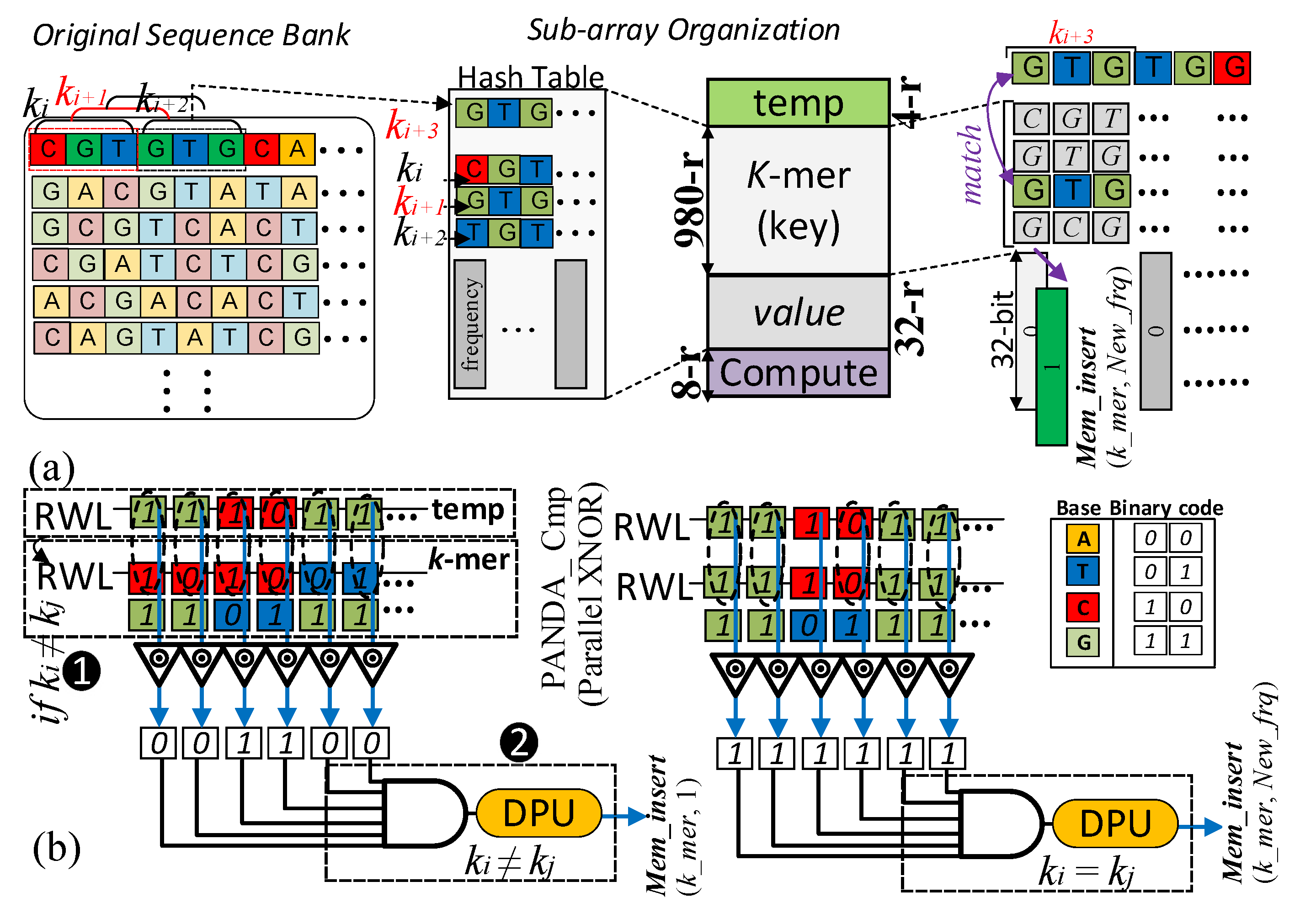
3.1. Stage One: Hash Table
| Algorithm 1 Procedure Hashmap (S, k) |
|
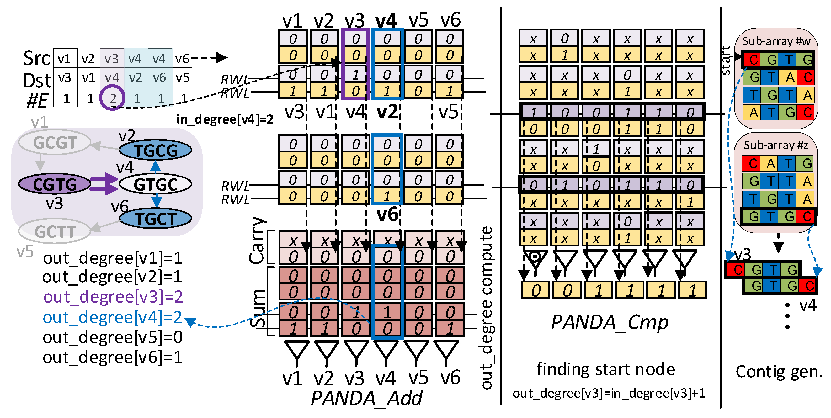
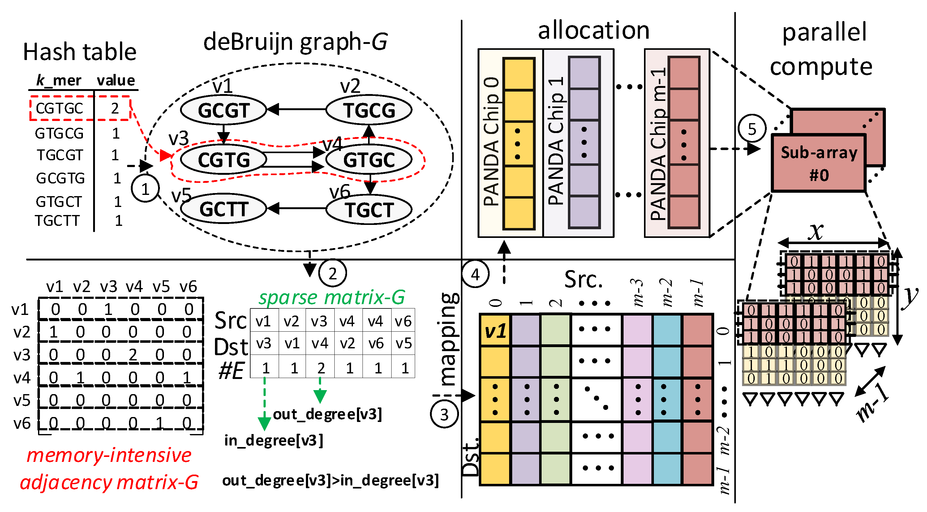
3.2. Stage Two: Graph Construction
| Algorithm 2 Procedure de Bruijn (Hashmap, k) |
|
3.3. Stage Three: Traversal for Euler Path
| Algorithm 3 Procedure find start vertex (G) |
|
| Algorithm 4 Procedure Fleury (G, node, edge_count, out_degree) |
|
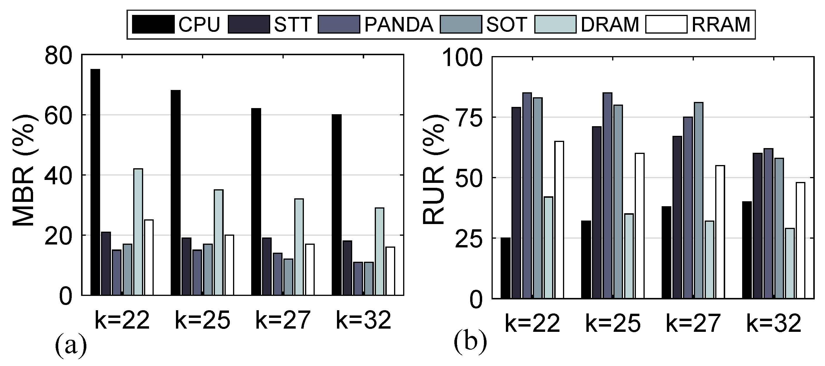
4. Performance Estimation
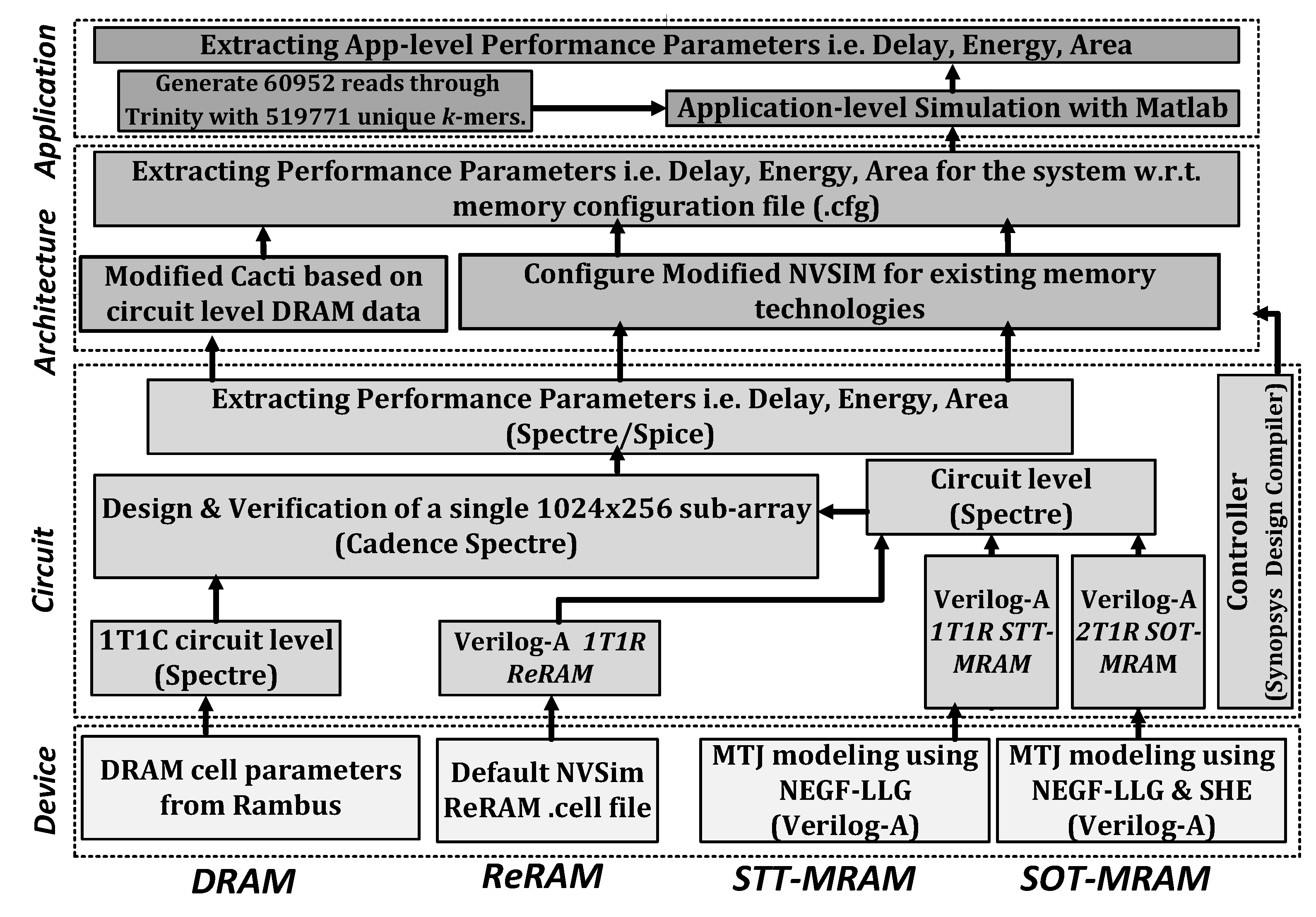
4.1. Setup
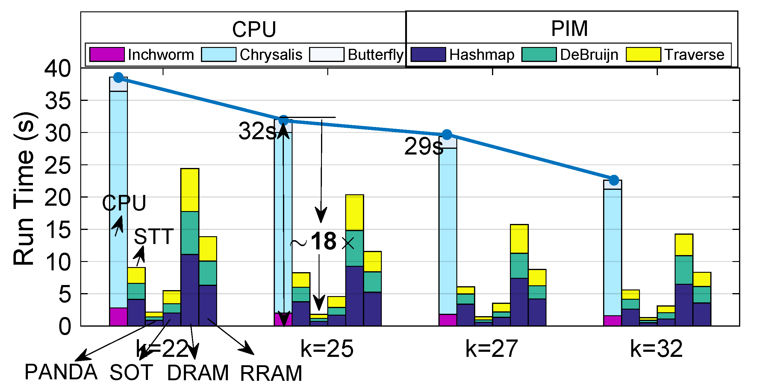
4.2. Run Time
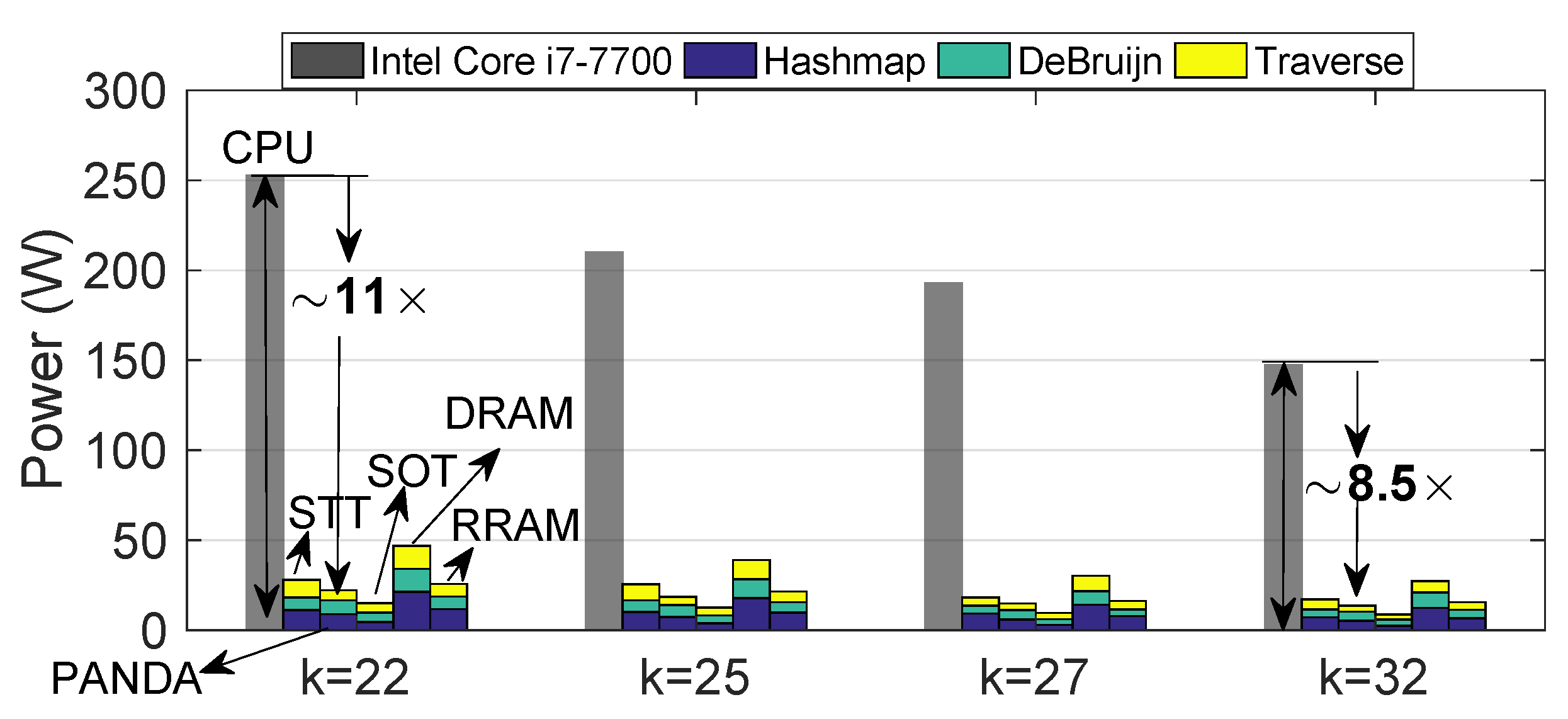
4.3. Power Consumption
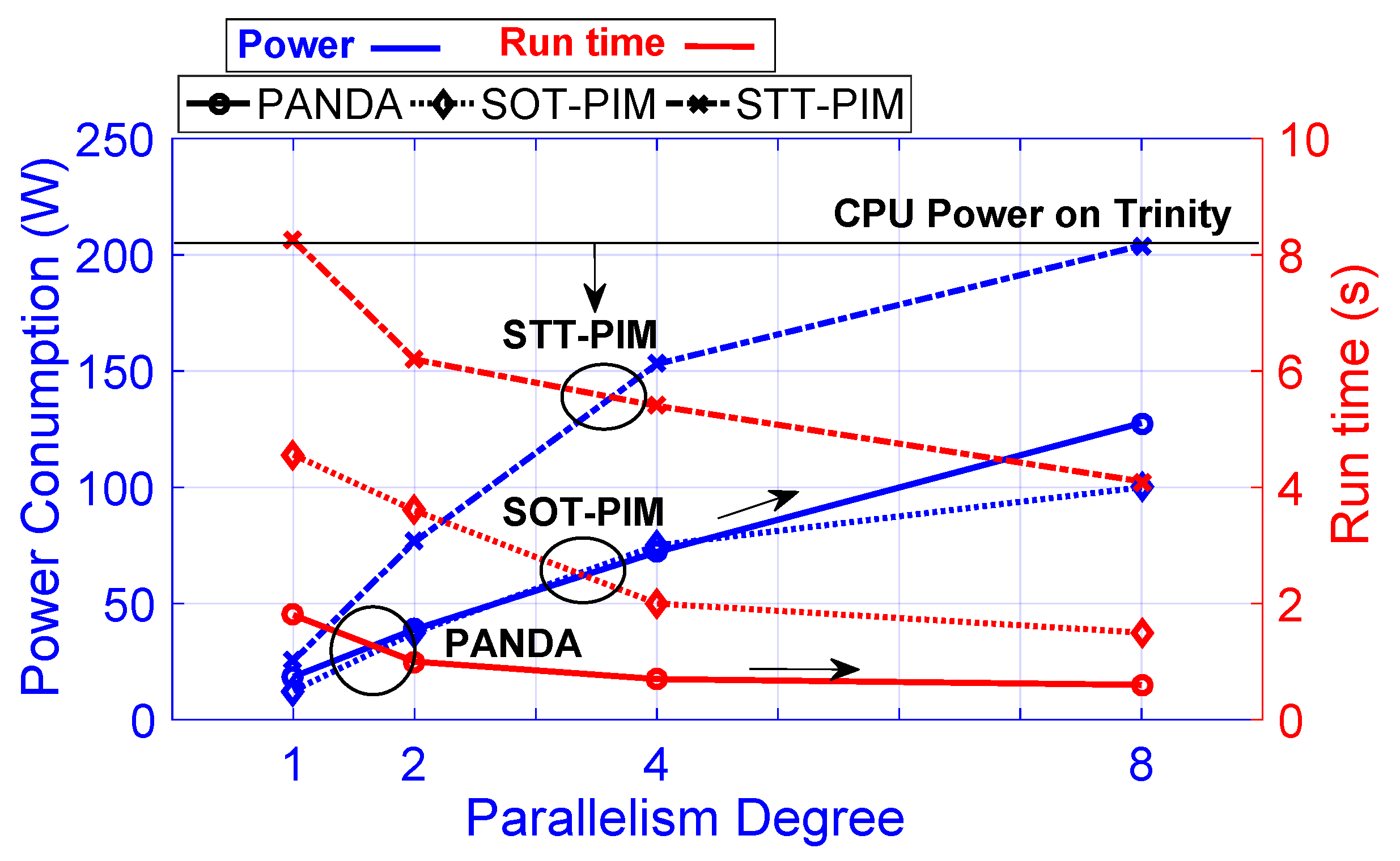
4.4. Speed-Up/Power Efficiency Trade-Off
4.5. Memory Wall Challenge
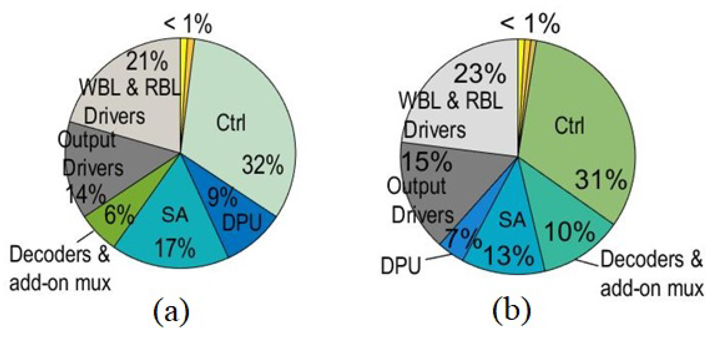
4.6. Area Overhead
5. Conclusions
Author Contributions
Funding
Data Availability Statement
Conflicts of Interest
References
- Li, H.; Homer, N. A survey of sequence alignment algorithms for next-generation sequencing. Brief. Bioinform. 2010, 11, 473–483. [Google Scholar] [CrossRef] [PubMed]
- Georganas, E.; Buluç, A.; Chapman, J.; Oliker, L.; Rokhsar, D.; Yelick, K. Parallel de bruijn graph construction and traversal for de novo genome assembly. In Proceedings of the SC’14: Proceedings of the International Conference for High Performance Computing, Networking, Storage and Analysis, New Orleans, LA, USA, 16–21 November 2014; IEEE: New York, NY, USA, 2014; pp. 437–448. [Google Scholar]
- Sinha, A.; Yang, H.-C.; Liu, P.-Y.; Kuo, Y.-S.; Fang, Y.; Chang, T.-S.; Li, K.-H.; Lai, B.-C. DSIM: Distributed Sequence Matching on Near-DRAM Accelerator for Genome Assembly. J. Emerg. Sel. Top. Circuits Syst. 2022, 12, 486–499. [Google Scholar] [CrossRef]
- Chapman, J.A.; Ho, I.; Sunkara, S.; Luo, S.; Schroth, G.P.; Rokhsar, D.S. Meraculous: De novo genome assembly with short paired-end reads. PLoS ONE 2011, 6, e23501. [Google Scholar] [CrossRef] [PubMed]
- Zokaee, F.; Zarandi, H.R.; Jiang, L. Aligner: A process-in-memory architecture for short read alignment in rerams. IEEE Comput. Archit. Lett. 2018, 17, 237–240. [Google Scholar] [CrossRef]
- Angizi, S.; Sun, J.; Zhang, W.; Fan, D. AlignS: A processing-in-memory accelerator for DNA short read alignment leveraging SOT-MRAM. In Proceedings of the 2019 56th ACM/IEEE Design Automation Conference (DAC), Las Vegas, NV, USA, 2–6 June 2019; pp. 1–6. [Google Scholar]
- Shahroodi, T.; Miao, M.; Lindegger, J.; Wong, S.; Mutlu, O.; Hamdioui, S. An In-Memory Architecture for High-Performance Long-Read Pre-Alignment Filtering. arXiv 2023, arXiv:2310.15634. [Google Scholar]
- Rumpf, M.D.; Alser, M.; Gollwitzer, A.E.; Lindegger, J.; Almadhoun, N.; Firtina, C.; Mangul, S.; Mutlu, O. SequenceLab: A Comprehensive Benchmark of Computational Methods for Comparing Genomic Sequences. arXiv 2023, arXiv:2310.16908. [Google Scholar]
- De Sandre, G.; Bettini, L.; Pirola, A.; Marmonier, L.; Pasotti, M.; Borghi, M.; Mattavelli, P.; Zuliani, P.; Scotti, L.; Mastracchio, G.; et al. A 90 nm 4 Mb embedded phase-change memory with 1.2 V 12 ns read access time and 1MB/s write throughput. In . In Proceedings of the 2010 IEEE International Solid-State Circuits Conference-(ISSCC), San Francisco, CA, USA, 7–11 February 2010. [Google Scholar]
- Tsuchida, K.; Inaba, T.; Fujita, K.; Ueda, Y.; Shimizu, T.; Asao, Y.; Kajiyama, T.; Iwayama, M.; Sugiura, K.; Ikegawa, S.; et al. A 64 Mb MRAM with clamped-reference and adequate-reference schemes. In Proceedings of the 2010 IEEE International Solid-State Circuits Conference-(ISSCC), San Francisco, CA, USA, 7–11 February 2010. [Google Scholar]
- Chang, M.F.; Shen, S.J.; Liu, C.C.; Wu, C.W.; Lin, Y.F.; King, Y.C.; Yamauchi, H. An Offset-Tolerant Fast-Random-Read Current-Sampling-Based Sense Amplifier for Small-Cell-Current Nonvolatile Memory. J. Solid-State Circuits 2013, 48, 864–877. [Google Scholar] [CrossRef]
- Seshadri, V.; Lee, D.; Mullins, T.; Hassan, H.; Boroumand, A.; Kim, J.; Kozuch, M.A.; Mutlu, O.; Gibbons, P.B.; Mowry, T.C. Ambit: In-memory accelerator for bulk bitwise operations using commodity DRAM technology. In Proceedings of the 2017 50th Annual IEEE/ACM International Symposium on Microarchitecture (MICRO), New York, NY, USA, 14–18 October 2017; pp. 273–287. [Google Scholar]
- Yu, J.; Nane, R.; Ashraf, I.; Taouil, M.; Hamdioui, S.; Corporaal, H.; Bertels, K. Skeleton-based Synthesis Flow for Computation-In-Memory Architectures. IEEE Trans. Emerg. Top. Comput. 2017, 2, 545–558. [Google Scholar] [CrossRef]
- Zhang, F.; Angizi, S.; Fahmi, N.A.; Zhang, W.; Fan, D. PIM-Quantifier: A Processing-in-Memory Platform for mRNA Quantification. In Proceedings of the 2021 58th ACM/IEEE Design Automation Conference (DAC), San Francisco, CA, USA, 5–9 December 2021; pp. 43–48. [Google Scholar]
- Li, S.; Xu, C.; Zou, Q.; Zhao, J.; Lu, Y.; Xie, Y. Pinatubo: A processing-in-memory architecture for bulk bitwise operations in emerging non-volatile memories. In Proceedings of the 53rd Annual Design Automation Conference, New York, NY, USA, 5–9 June 2016; pp. 1–6. [Google Scholar]
- Chowdhury, Z.I.; Zabihi, M.; Khatamifard, S.K.; Zhao, Z.; Resch, S.; Razaviyayn, M.; Wang, J.P.; Sapatnekar, S.S.; Karpuzcu, U.R. A DNA Read Alignment Accelerator Based on Computational RAM. IEEE J. Explor. Solid-State Comput. Devices Circuits 2020, 6, 80–88. [Google Scholar] [CrossRef]
- Kang, W.; Wang, H.; Wang, Z.; Zhang, Y.; Zhao, W. In-memory processing paradigm for bitwise logic operations in STT–MRAM. IEEE Trans. Magn. 2017, 53, 1–4. [Google Scholar]
- Angizi, S.; Sun, J.; Zhang, W.; Fan, D. GraphS: A graph processing accelerator leveraging SOT-MRAM. In Proceedings of the 2019 Design, Automation & Test in Europe Conference & Exhibition (DATE), Florence, Italy, 25–29 March 2019; pp. 378–383. [Google Scholar]
- Li, R.; Yu, C.; Li, Y.; Lam, T.W.; Yiu, S.M.; Kristiansen, K.; Wang, J. SOAP2: An improved ultrafast tool for short read alignment. Bioinformatics 2009, 25, 1966–1967. [Google Scholar] [CrossRef] [PubMed]
- Richard Wilton, A.S.S. Performance optimization in DNA short-read alignment. Bioinformatics 2022, 38, 2081–2087. [Google Scholar] [CrossRef] [PubMed]
- Liu, C.M.; Wong, T.; Wu, E.; Luo, R.; Yiu, S.M.; Li, Y.; Wang, B.; Yu, C.; Chu, X.; Zhao, K.; et al. SOAP3: Ultra-fast GPU-based parallel alignment tool for short reads. Bioinformatics 2012, 28, 878–879. [Google Scholar] [CrossRef] [PubMed]
- Arram, J.; Kaplan, T.; Luk, W.; Jiang, P. Leveraging FPGAs for accelerating short read alignment. IEEE/ACM Trans. Comput. Biol. Bioinform. 2016, 14, 668–677. [Google Scholar] [CrossRef] [PubMed]
- Mahmood, S.F.; Rangwala, H. Gpu-euler: Sequence assembly using gpgpu. In Proceedings of the 2011 IEEE International Conference on High Performance Computing and Communications, Banff, AB, Canada, 2–4 September 2011; pp. 153–160. [Google Scholar]
- Varma, B.S.C.; Paul, K.; Balakrishnan, M. FPGA-Based Acceleration of De Novo Genome Assembly. In Architecture Exploration of FPGA Based Accelerators for BioInformatics Applications; Springer: Berlin/Heidelberg, Germany, 2016; pp. 55–79. [Google Scholar]
- Zerbino, D.R.; Birney, E. Velvet: Algorithms for de novo short read assembly using de Bruijn graphs. Genome Res. 2008, 18, 821–829. [Google Scholar] [CrossRef]
- Grabherr, M.G.; Haas, B.J.; Yassour, M.; Levin, J.Z.; Thompson, D.A.; Amit, I.; Adiconis, X.; Fan, L.; Raychowdhury, R.; Zeng, Q.; et al. Full-length transcriptome assembly from RNA-Seq data without a reference genome. Nat. Biotechnol. 2011, 29, 644–652. [Google Scholar] [CrossRef] [PubMed]
- Goswami, S.; Lee, K.; Shams, S.; Park, S.J. Gpu-accelerated large-scale genome assembly. In Proceedings of the 2018 IEEE International Parallel and Distributed Processing Symposium (IPDPS), Vancouver, BC, Canada, 21–25 May 2018; pp. 814–824. [Google Scholar]
- Ren, S.; Ahmed, N.; Bertels, K.; Al-Ars, Z. An Efficient GPU-Based de Bruijn Graph Construction Algorithm for Micro-Assembly. In Proceedings of the 2018 IEEE 18th International Conference on Bioinformatics and Bioengineering (BIBE), Taichung, Taiwan, 29–31 October 2018; pp. 67–72. [Google Scholar]
- Lu, M.; Luo, Q.; Wang, B.; Wu, J.; Zhao, J. GPU-accelerated bidirected De Bruijn graph construction for genome assembly. In Proceedings of the Asia-Pacific Web Conference, Sydney, Australia, 4–6 April 2013; pp. 51–62. [Google Scholar]
- Angizi, S.; Fahmi, N.A.; Zhang, W.; Fan, D. PIM-Assembler: A processing-in-memory platform for genome assembly. In Proceedings of the 2020 57th ACM/IEEE Design Automation Conference (DAC), San Francisco, CA, USA, 20–24 July 2020; pp. 1–6. [Google Scholar]
- Angizi, S. Processing-in-Memory for Data-Intensive Applications, from Device to Algorithm. Ph.D. Thesis, Arizona State University, Tempe, AZ, USA, 2021. [Google Scholar]
- Fong, X.; Kim, Y.; Yogendra, K.; Fan, D.; Sengupta, A.; Raghunathan, A.; Roy, K. Spin-transfer torque devices for logic and memory: Prospects and perspectives. IEEE Trans. Comput.-Aided Des. Integr. Circuits Syst. 2015, 35, 1–22. [Google Scholar] [CrossRef]
- Pai, C.F.; Liu, L.; Li, Y.; Tseng, H.; Ralph, D.; Buhrman, R. Spin transfer torque devices utilizing the giant spin Hall effect of tungsten. Appl. Phys. Lett. 2012, 101, 122404. [Google Scholar] [CrossRef]
- Razavi, B. The StrongARM latch [a circuit for all seasons]. IEEE Solid-State Circuits Mag. 2015, 7, 12–17. [Google Scholar] [CrossRef]
- Yuasa, S.; Nagahama, T.; Fukushima, A.; Suzuki, Y.; Ando, K. Giant room-temperature magnetoresistance in single-crystal Fe/MgO/Fe magnetic tunnel junctions. Nat. Mater. 2004, 3, 868. [Google Scholar] [CrossRef]
- Mutlu, O.; Ghose, S.; Gómez-Luna, J.; Ausavarungnirun, R. A Modern Primer on Processing in Memory. arXiv 2020, arXiv:2012.03112. [Google Scholar]
- Patel, M.; Kim, J.S.; Hassan, H.; Mutlu, O. Understanding and modeling on-die error correction in modern DRAM: An experimental study using real devices. In Proceedings of the 2019 49th Annual IEEE/IFIP International Conference on Dependable Systems and Networks (DSN), Portland, OR, USA, 24–24 June 2019; pp. 13–25. [Google Scholar]
- Li, R.; Zhu, H.; Ruan, J.; Qian, W.; Fang, X.; Shi, Z.; Li, Y.; Li, S.; Shan, G.; Kristiansen, K.; et al. De novo assembly of human genomes with massively parallel short read sequencing. Genome Res. 2010, 20, 265–272. [Google Scholar] [CrossRef]
- Simpson, J.T.; Wong, K.; Jackman, S.D.; Schein, J.E.; Jones, S.J.; Birol, I. ABySS: A parallel assembler for short read sequence data. Genome Res. 2009, 19, 1117–1123. [Google Scholar] [CrossRef] [PubMed]
- Dai, G.; Huang, T.; Chi, Y.; Zhao, J.; Sun, G.; Liu, Y.; Wang, Y.; Xie, Y.; Yang, H. Graphh: A processing-in-memory architecture for large-scale graph processing. IEEE Trans. Comput.-Aided Des. Integr. Circuits Syst. 2018, 38, 640–653. [Google Scholar] [CrossRef]
- Jain, S.; Ranjan, A.; Roy, K.; Raghunathan, A. Computing in memory with spin-transfer torque magnetic RAM. IEEE Trans. Very Large Scale Integr. (VLSI) Syst. 2017, 26, 470–483. [Google Scholar] [CrossRef]
- Imani, M.; Kim, Y.; Rosing, T. Mpim: Multi-purpose in-memory processing using configurable resistive memory. In Proceedings of the 2017 22nd Asia and South Pacific Design Automation Conference (ASP-DAC), Chiba, Japan, 16–19 January 2017; pp. 757–763. [Google Scholar]
- Synopsys Inc. Synopsys Design Compiler, Product Version 14.9.2014; Synopsys Inc.: Sunnyvale, CA, USA, 2014. [Google Scholar]


| Operations | Active SA | Row Init. (1) | ||||
|---|---|---|---|---|---|---|
| Read | 0 | 0 | 0 | 1 | SA-III | No |
| (N)AND3/(N)AND2 | 1 | 0 | 0 | 0 | SA-III | No/Yes |
| (N)OR3/(N)OR2 | 0 | 0 | 1 | 0 | SA-I | No/Yes |
| X(N)OR2 | 1 | 1 | 1 | 0 | SA-I-II-III | Yes |
| Maj (Carry)/Min | 0 | 1 | 0 | 0 | SA-II | No |
| XOR3 (Sum) | 1 | 1 | 1 | 0 | SA-I-II-III | No |
| Parameter | Value |
|---|---|
| Free layer dimension | nm3 |
| SHM dimension | nm3 |
| Demagnetization factor, ; ; | 0.066; 0.911; 0.022 |
| Spin flip length, | 1.4 nm |
| Spin Hall angle, | 0.3 |
| Gilbert damping factor, | 0.007 |
| Saturation magnetization, | 850 kA/m |
| Oxide thickness, | 1.2 nm |
| RA product, / | 10.58 m2/ |
| Supply voltage | 1 V |
| CMOS technology | 45 nm |
| SOT-MRAM cell area | 69 F2 |
| Access transistor width | 4.5 F |
| Cell aspect ratio | 1.91 |
| Designs | Area (mm2) | Dynamic Energy (nJ) | Latency (ns) | Leak. Power (mW) | ||||||
|---|---|---|---|---|---|---|---|---|---|---|
| R | W | C-AND3 | C-Add | R | W | C-AND3 | C-Add | |||
| Standard | 7.06 | 0.57 | 0.66 | - | - | 3.85 | 4.5 | - | - | 402 |
| PANDA | 9.3 | 0.78 | 0.69 | 0.85 | 1.93 | 3.91 | 4.59 | 3.91 | 3.91 | 586 |
Disclaimer/Publisher’s Note: The statements, opinions and data contained in all publications are solely those of the individual author(s) and contributor(s) and not of MDPI and/or the editor(s). MDPI and/or the editor(s) disclaim responsibility for any injury to people or property resulting from any ideas, methods, instructions or products referred to in the content. |
© 2024 by the authors. Licensee MDPI, Basel, Switzerland. This article is an open access article distributed under the terms and conditions of the Creative Commons Attribution (CC BY) license (https://creativecommons.org/licenses/by/4.0/).
Share and Cite
Angizi, S.; Fahmi, N.A.; Najafi, D.; Zhang, W.; Fan, D. PANDA: Processing in Magnetic Random-Access Memory-Accelerated de Bruijn Graph-Based DNA Assembly. J. Low Power Electron. Appl. 2024, 14, 9. https://doi.org/10.3390/jlpea14010009
Angizi S, Fahmi NA, Najafi D, Zhang W, Fan D. PANDA: Processing in Magnetic Random-Access Memory-Accelerated de Bruijn Graph-Based DNA Assembly. Journal of Low Power Electronics and Applications. 2024; 14(1):9. https://doi.org/10.3390/jlpea14010009
Chicago/Turabian StyleAngizi, Shaahin, Naima Ahmed Fahmi, Deniz Najafi, Wei Zhang, and Deliang Fan. 2024. "PANDA: Processing in Magnetic Random-Access Memory-Accelerated de Bruijn Graph-Based DNA Assembly" Journal of Low Power Electronics and Applications 14, no. 1: 9. https://doi.org/10.3390/jlpea14010009
APA StyleAngizi, S., Fahmi, N. A., Najafi, D., Zhang, W., & Fan, D. (2024). PANDA: Processing in Magnetic Random-Access Memory-Accelerated de Bruijn Graph-Based DNA Assembly. Journal of Low Power Electronics and Applications, 14(1), 9. https://doi.org/10.3390/jlpea14010009