Article

Class AB Voltage Follower and Low-Voltage Current Mirror with Very High Figures of Merit Based on the Flipped Voltage Follower

by
Jaime Ramírez-Angulo
1,*,
Anindita Paul
2,
Manaswini Gangineni
3,
Jose Maria Hinojo-Montero
4 and
Jesús Huerta-Chua
1
1
Electronic Engineering Department, Instituto Tecnologico Superior de Poza Rica, Poza Rica 93230, Mexico
2
Department of Computer Science and Electronics, Morehead State University, Morehead, KY 40351, USA
3
Klipsch School of Electrical and Computer Electrical Engineering, New Mexico State University, MSC 3-O, P.O. Box 30001, Las Cruces, NM 88003-8001, USA
4
Department of Electronic Engineering, University of Seville, 41092 Seville, Spain
*
Author to whom correspondence should be addressed.
J. Low Power Electron. Appl. 2023, 13(2), 28; https://doi.org/10.3390/jlpea13020028
Submission received: 20 March 2023 / Revised: 19 April 2023 / Accepted: 20 April 2023 / Published: 24 April 2023

Abstract

:
The application of the flipped voltage follower to implement two high-performance circuits is presented: (1) The first is a class AB cascode flipped voltage follower that shows an improved slew rate and an improved bandwidth by very large factors and that has a higher output range than the conventional flipped voltage follower. It has a small signal figure of merit FOMSS = 46 MHz pF/µW and a current efficiency figure of merit FOMCE = 118. This is achieved by just introducing an additional output current sourcing PMOS transistor (P-channel Metal Oxide Semiconductor Field Effect Transistor) that provides dynamic output current enhancement and increases the quiescent power dissipation by less than 10%. (2) The other is a high-performance low-voltage current mirror with a nominal gain accuracy better than 0.01%, 0.212 Ω input resistance, 112 GΩ output resistance, 1 V supply voltage requirements, 0.15 V input, and 0.2 V output compliance voltages. These characteristics are achieved by utilizing two auxiliary amplifiers and a level shifter that increase the power dissipation just moderately. Post-layout simulations verify the performance of the circuits in a commercial 180 nm CMOS (Complementary Metal Oxide Semiconductor) technology.

1. Introduction

Two of the basic building blocks of analog integrated circuits are the voltage follower and the current mirror. The conventional common-drain amplifier or voltage follower (denoted here as CONV_VF)) [1,2,3] of Figure 1a has been used for many years as a buffer due to its infinite input resistance, medium–low output impedance Rout = 1/gm (in the order of tens of kΩs) close to the unity voltage gain, and relatively high bandwidth BW = gm/(2π CL). The flipped voltage follower of Figure 1b [4] is an improved voltage follower that uses local negative feedback to provide lower output resistance Rout = 1/[gm(gmro)] = 1/(gmA) (hundreds of Ω), where CL is the load capacitance, gm and ro are the transconductance gain and output resistance, and A = gmro is the intrinsic gain of the MOS transistor. The basic Flipped Voltage Follower(FVF) version of Figure 1b (denoted here as CONV_FVF) suffers the serious limitation that it has a very low peak-to-peak output swing Voswingpp, which is independent of the supply voltage and given by Voswingpp = VTH − VDSsat (where VTH is the threshold voltage and VDSsat is the drain-source saturation voltage of MFVF). It operates in class A with a peak positive output current and positive slew rate limited by the bias current Ibias to a value SR+ = Ibias/CL. Several versions of the flipped voltage follower have been reported with improved output range and lower output resistance. For example, the cascode FVF (denoted here as CONV_CSCFVF) shown in Figure 1c and reported in [5] uses an additional branch with a cascode transistor MCAS that increases the local feedback loop gain and provides even lower output resistance by a factor A = gmro so that, in this circuit, Rout = 1/[gm(gmro)2] = 1/[gmA2] (on the order of tens of Ωs). It also has an increased output swing, which is dependent on the supply voltage and given by Voutswingpp = VDD − (VGS + VDSsat) = VDD − VTH − 2VDSsat. The cascode FVF of Figure 1c (denoted here as CONV_CSCFVF) is a class A circuit with a positive slew rate seriously limited by the bias current to a value: SR+ = Ibias/CL. Class AB versions of the FVF have also been reported [6,7,8,9] to overcome this limitation to a certain degree.
The low-voltage cascode current mirror of Figure 2a (denoted here as CN_CS_CM) has been used for many years as a high-bandwidth linear current amplifier. It has a moderately low input resistance Rin = 1/gm (on the order of tens of kΩs), moderately high output resistance Rout = ro(gmro) = roA (on the order of tens of MΩs), high linearity, low gain error, low output compliance voltage (Voutmin = 2VDSSat), and moderate input voltage requirements Vin = VGS = VTH + VDssat. A simple rearrangement of the circuit of Figure 2a is shown in Figure 2b. It injects the input current source Iin at the source of the cascode transistor M1C (node Vx) instead of at its drain (node Vy). This reduces the input voltage requirements from VGS to VDSsat and leads to a reduction in the input resistance by a factor A from Rin = 1/gm to Rin = 1/[gm(gmro)] = 1/[gmA]. Notice that, in this circuit, the input transistors M1 and M1C form a flipped voltage follower with a constant input voltage Vcn at the gate of M1C and the current input signal Iin injected at the output terminal of the FVF (node Vx). In spite of the improvement in the mirror characteristics, this modification suffers from a non-linear current mirror gain resulting from lambda effect and unequal drain source voltages in the input and output transistors M1 and M2 of the current mirror. This is due to the fact that the cascode input and output transistors M1C and M2C have unequal drain currents which cause their gate-source voltages to be different. The gate source voltages of M1C and M2C determine the drain-source voltages of M1 and M2 and the linearity of the mirror. This effect can be greatly mitigated in a BiCMOS process by replacing the cascode transistors by bipolar transistors.
In this paper, the authors introduce two improved circuits based on the flipped voltage follower: (1) a power-efficient class AB cascode FVF (denoted here as HP_CSCFVF) with high swing, very low output resistance, and essentially higher small signal and large signal figures of merit than previously reported AB FVF versions and (2) a low-voltage high-performance cascoded current mirror (denoted here as HP_CS_CM) with much lower input resistance and much higher output resistance than the conventional current mirror and highly linear gain. The proposed circuits are described in Section 2. Section 3 shows the post-layout simulation results that verify the high-performance characteristics of the proposed circuits, and Section 4 provides the conclusions.

2. Proposed Circuits

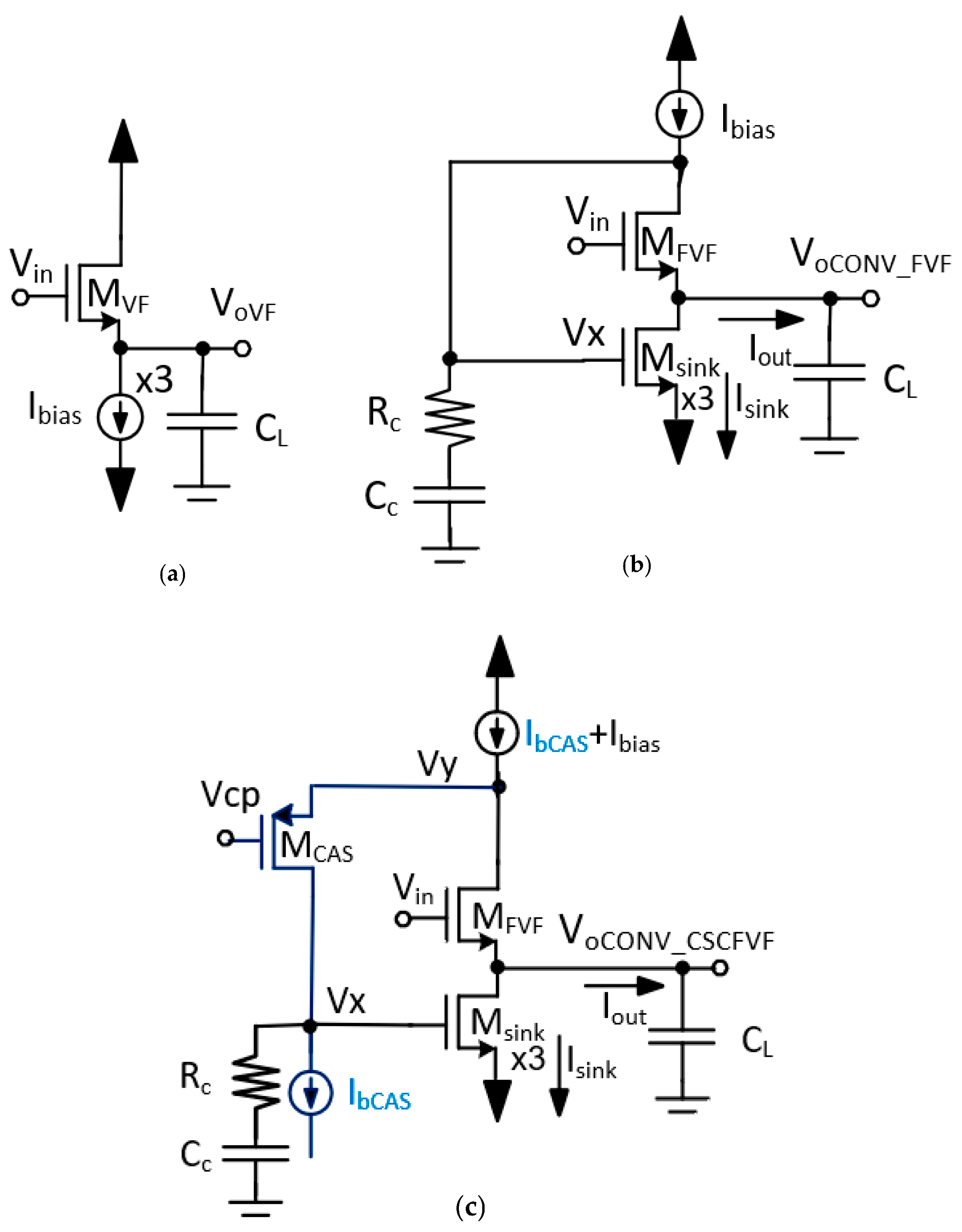
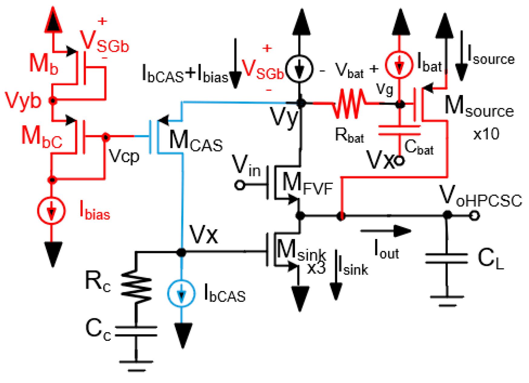
2.1. High-Performance Class AB Voltage Follower HP_CSCFVF

2.1.1. Description

Figure 3 shows the scheme of the proposed class AB high-performance cascode FVF (HP_CSCFVF). It is a modification of the class A cascode FVF reported in [5] and is shown in Figure 1c. It includes an additional branch with a PMOS transistor Msource that provides efficient class AB operation. Msource has a small quiescent current IQsource, but it can inject positive output currents Iout into the load CL, which are much larger than IQsource. On the other hand, transistor Msink can sink very large negative load currents (also much larger than the quiescent current of Msink given by IQsink = IQsource + Ibias), as is discussed below. The biasing branch has two diode-connected PMOS transistors Mb and MbC. Based on replica biasing, this branch sets the voltage Vy to a value Vy = VDD − VSGb and the gate voltage of Msource to a value Vg = Vy + Vbat, where Vbat = IbatRbat. The values of Ibat and Rbat are selected so that Vbat has an approximate value Vbat = VSDsat = 0.1 V. In this case, the quiescent source-gate voltage of Msource is given by VQSGsource = VSGb − IbatRbat. This leads to a quiescent voltage VQSGsource = VSGb − VSDsat ≈ VTH close to the threshold voltage of Msource. This quiescent source-gate voltage sets a relatively small quiescent current IQsource in Msource, which is independent of the supply voltage. A capacitor Cbat forms a high-pass filter with Rbat and Cbat. This is used to transfer fast transient variations from Vx to the gate Vg of Msource.

2.1.2. Class AB Operation of Proposed Voltage Follower

For positive input voltage variations in Vin, the output voltage VoHPCSC increases, and the gate voltage Vx of Msink decreases. The current in Msink decreases (and eventually turns off) and the dynamic changes in Vx are transferred to Vg by Cbat to the gate of Msource. The decrease in Vg causes the current Isource of Msource to increase, providing a positive output current Iout that can be significantly larger than the quiescent current IQsource of Msource (in the design described in Section 3, IQsource has a value IQsource = 7 µA). For negative input voltages, the output voltage decreases, and Vx increases. This increases the current Isink and provides a large negative output current Iout that can be much larger than the quiescent current IQsink of Msink. The FVFs in Figure 1b,c and Figure 3 use an RC compensation network formed by Cc and Rc for the local feedback loop. These elements provide a dominant pole and a high-frequency zero at Vx that approximately match the output pole of the open loop gain ωpout = gmFVF/CL at the output node VoHPCSC. This allows FVF circuits to significantly improve their bandwidth with respect to the conventional voltage follower of Figure 1a. This simple but effective FVF compensation and bandwidth extension technique was reported in [10].

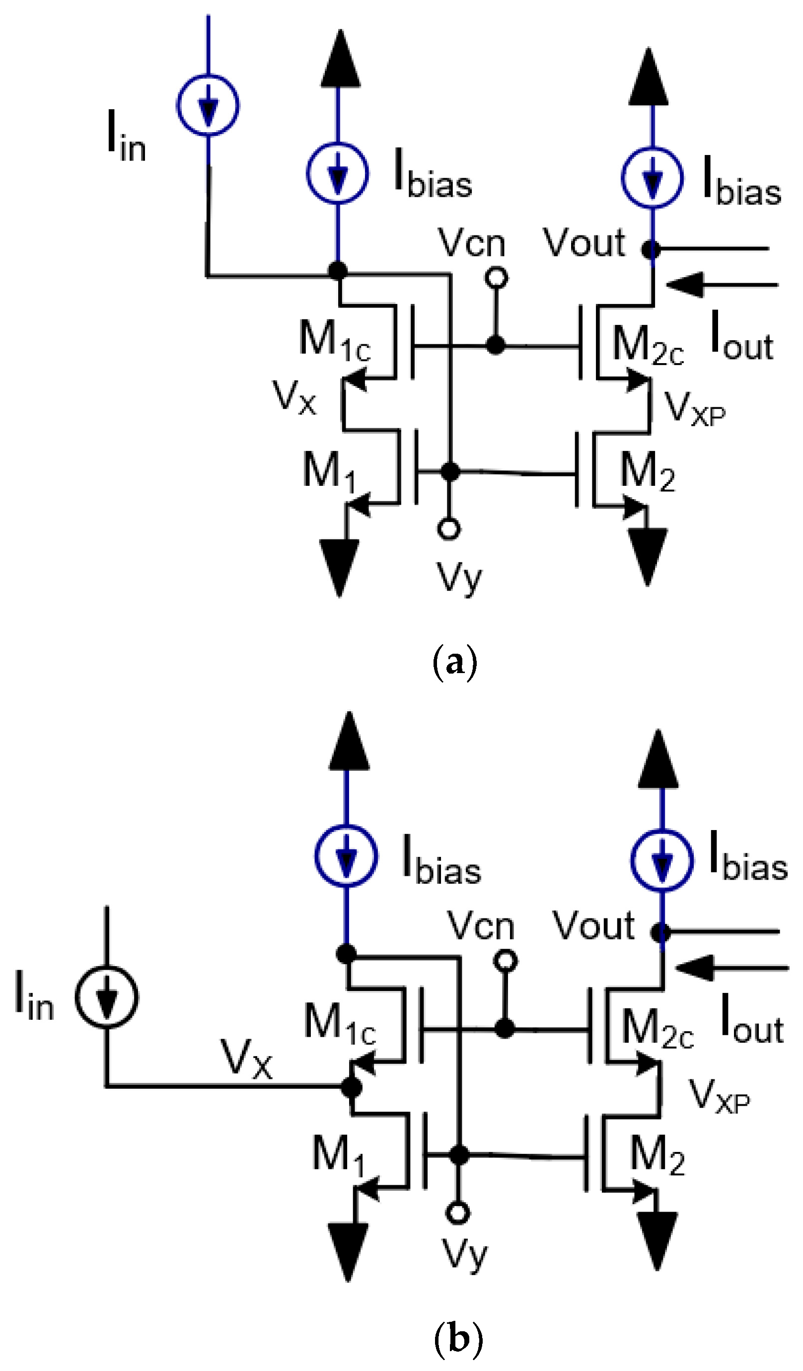
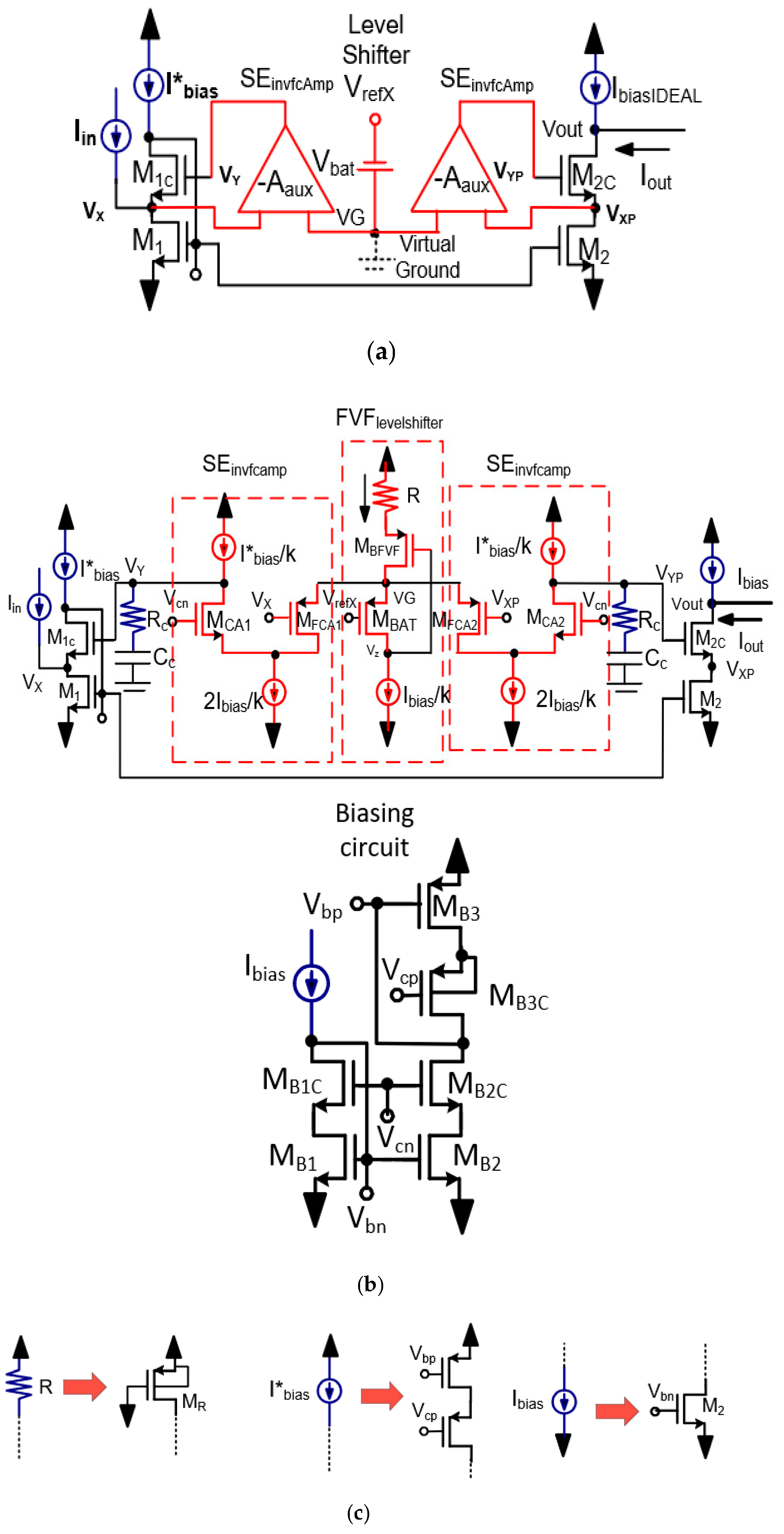
2.2. High-Performance Low-Voltage Current Mirror (HP_CS_CM)

The scheme of the proposed low-voltage high-performance current mirror (HP_CS_CM) is shown in Figure 4a. It is a modified version of the FVF current mirror of Figure 2b that includes two auxiliary amplifiers ASEinvfcamp with gain Aaux and a level shifter FVFlevelshifter. The transistor level implementation of the auxiliary amplifiers and the level shifter is shown in Figure 4b. Each of the amplifiers form local negative feedback loops with the cascode transistors M1C and M2C. They boost their effective gain by the gain Aaux = (gmro)2 = A2 of the auxiliary amplifiers. They are implemented in Figure 4b using single-ended folded cascode inverting amplifiers formed by MFCA1 and MCA1 and by MFCA2 and MCA2. A modified flipped voltage follower is used to generate a very-low-impedance node VG that operates as the signal ground (or reference node) for the input common source transistors MFCA1 and MFCA2 of the auxiliary amplifiers. Transistors MBAT, MFCA1, and MFCA2 have the same W/L dimensions, the same quiescent current, and quiescent gate-source voltages. For this reason, the negative feedback loops of the auxiliary amplifiers shown in Figure 4a,b cause the gate voltages VrefX, VX, and VXP to have the same value. This results in equal drain-source voltages of the input and output mirror transistors and leads to a highly linear and accurate current mirror gain. On the other hand, the large gain boosting of the cascode transistors M1C and M2C provided by the folded cascode auxiliary amplifiers leads to an extremely low input resistance Rin = 1/(gmA3)/2, which is lower by a factor of Aaux = A2/2 than the input resistance of the FVF mirror of Figure 2b and to an extremely high output resistance Rout = roA3 that is higher by the same factor Aaux than the output resistance of the mirrors of Figure 2. The value of VrefX (selected by the designer) sets the input voltage requirement Vin of the mirror. It must be higher than VDSsat in order to keep the input and output mirror transistors in saturation. In the proposed design, VrefX was selected to have a value VrefX = 0.15 V, but it can also have been lower since input and output transistors had a value VDSat = 0.06 V in the design discussed in Section 3. Remarks: (1) The FVF level shifter is a modified version of the basic FVF (or CONV_FVF). It has a resistor R in series with transistor MBFVF. This resistor R in Figure 4a is used to generate a voltage drop that pulls down the voltage at node Vz and allows transistor MBAT to have enough drain-source (VDS > VDSSat) voltage to operate in saturation. (2) The implementation of the auxiliary amplifiers using folded cascode amplifiers with a floating virtual ground node VG in which the nominal voltage is set by the designer has the purpose of reducing the supply requirements of the circuit. (3) A distinctive characteristic of the proposed mirror is that the modified FVF with resistor R allows the quiescent value of VG to be set to a value that is convenient to minimize the supply voltage and the input voltage requirements of the circuit. It also allows MBAT to be maintained in saturation. Previous implementations of mirrors with auxiliary amplifiers (i.e., the regulated cascode mirrors discussed in [1]) required the source of the auxiliary amplifier’s input transistors to be connected to one of the supply rails and does not allow the supply requirements to be minimized or Vin to be set. (4) If required, the gain Aaux of the auxiliary amplifiers can be further boosted from a value Aaux = A2/2 in the circuit of Figure 4b to a value Aaux = A3/2 by utilizing double-cascoded auxiliary amplifiers. This would also boost the output impedance by an additional factor A/2 and decrease the input impedance of the mirror by the same factor. (5) The local negative feedback loops formed by the auxiliary amplifiers have only one high-impedance node at VY and VYP. Compensation elements Rc and Cc are used to generate a dominant pole (and a zero) at these nodes. This is in order to compensate these loops and to prevent instability. (6) In order to reduce power dissipation, the auxiliary amplifiers and the FVF level shifters are biased with currents Ibias/k, which is a factor k times smaller than the bias current Ibias of the input and output mirror transistors M1 and M2. In the proposed design, a value k = 10 was used. This lead to a total quiescent current and power dissipation of the proposed mirror that is only 25% higher than the power dissipation of the mirrors of Figure 2. (7) The proposed current mirror can be easily transformed into a class AB mirror using the techniques reported in [11].

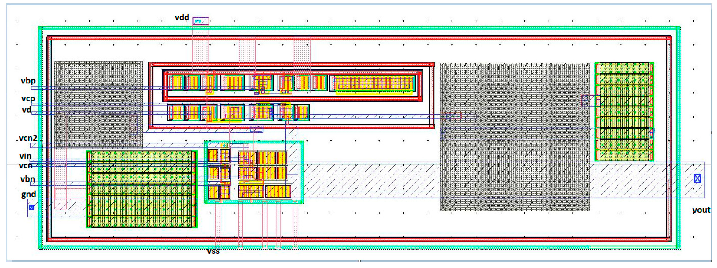
3. Simulation Results

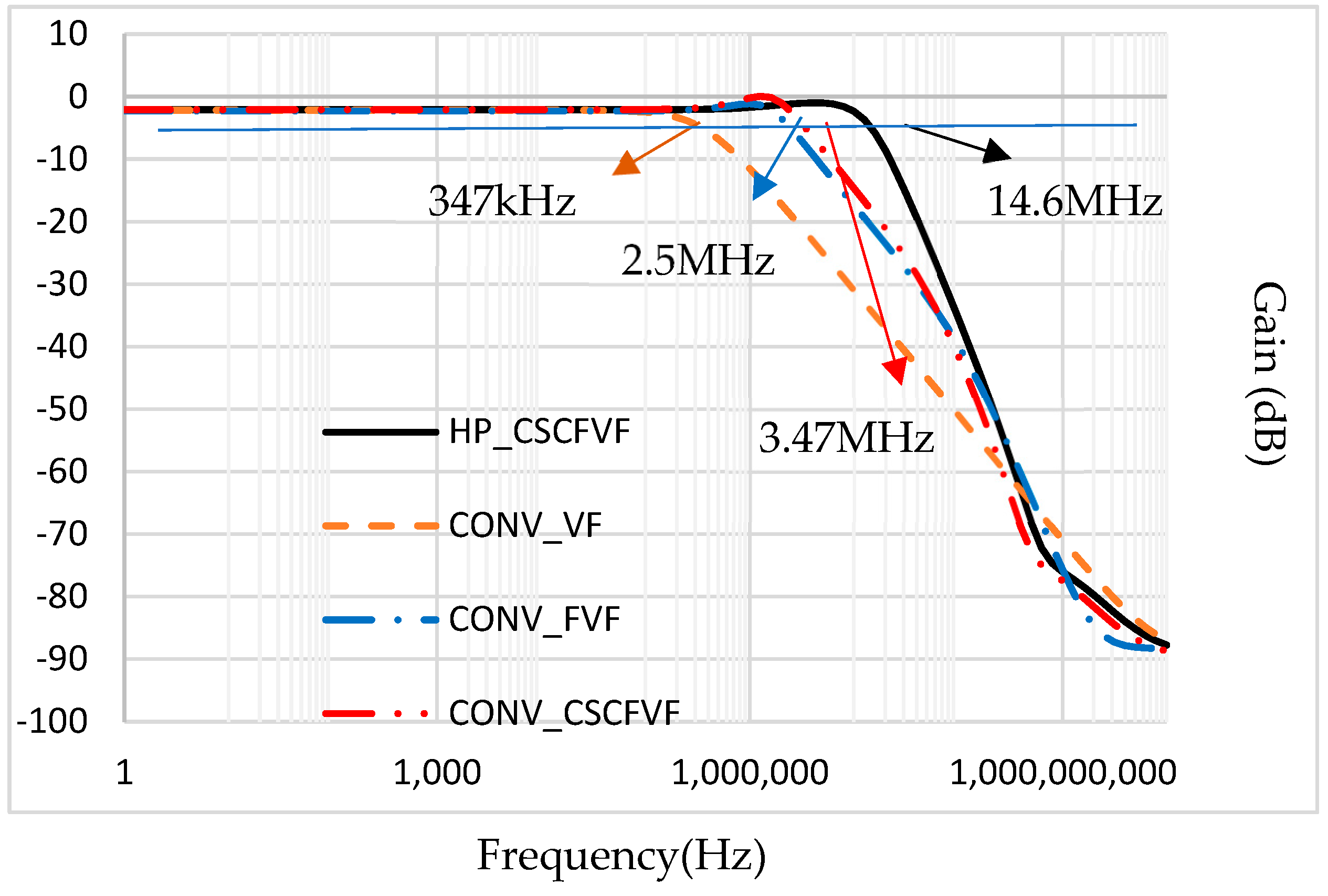
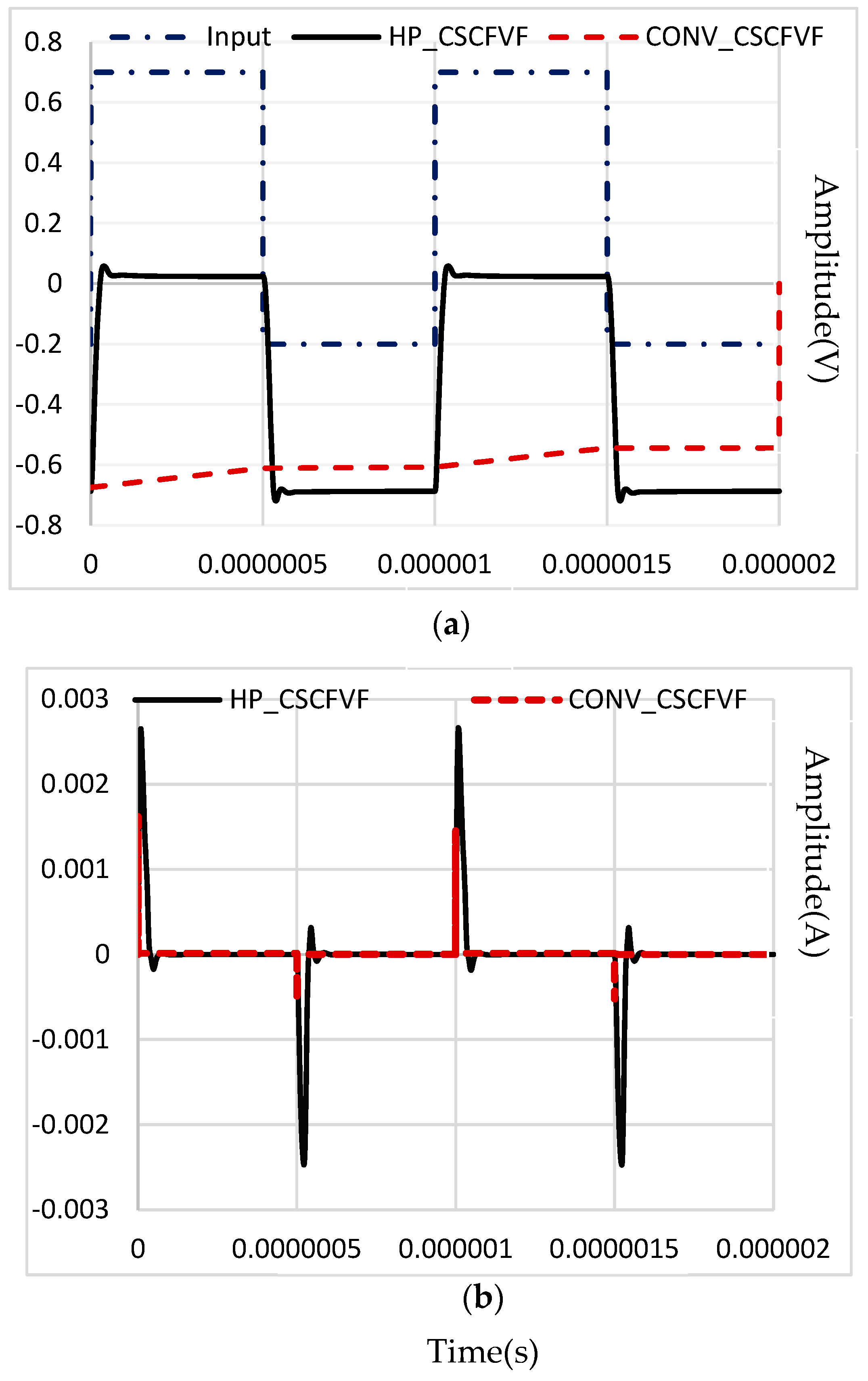
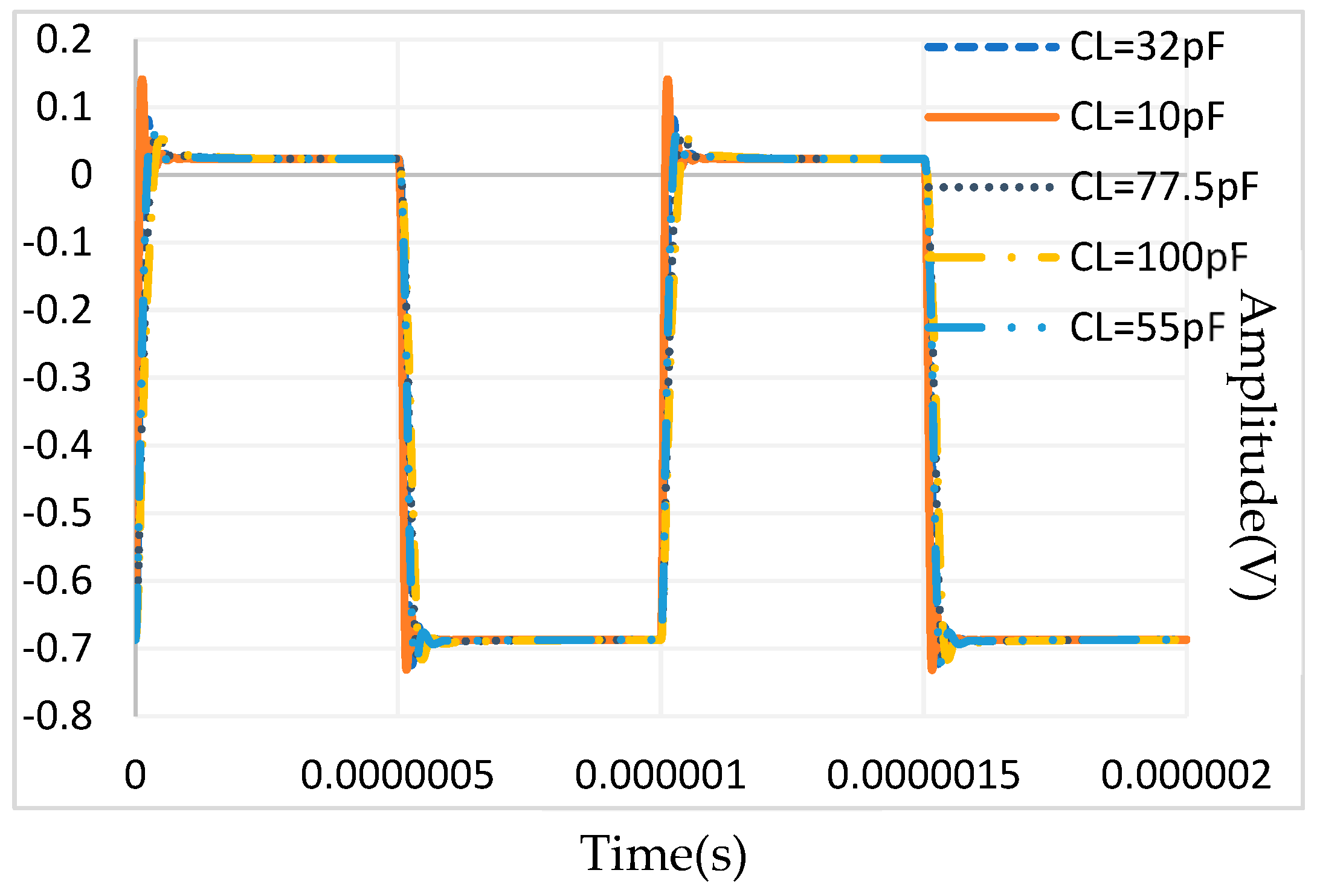
3.1. Simulations of the High-Perfromance Class AB Follower HP_CSCFVF

The CONV_VF, CONV_FVF, CONV_CSCFVF, and proposed HP_CSCFVF circuits of Figure 1a–c and Figure 3 were simulated in a commercial 180 nm CMOS technology with dual rail voltages VDD = 0.75 V, VSS = −0.75 V (or Vsupply = VDD − VSS = 1.5 V), Ibias = IbCAS = 5 µA, Rbat = 55 kΩ, Cbat = 2 pF, Ibat = 2 µA, CL = 100 pF, and W/L = 5/0.2 (µm) for all PMOS, and NMOS transistors, except the PMOS and NMOS transistors, implementing biasing sources that had dimensions W/L = 5/0.4 (µm), values Cc = 0.6 pF, and Rc = 75 kΩ were used. In order to save on silicon area, Rc was implemented with an NMOS transistor with W/L = 0.75/15 and with the gate connected to the positive rail VDD. Rc and Cc were selected to provide a dominant pole ωpdom = 1/RxCc at node VX: and a high-frequency zero ωz = 1/RcCc at Vx that approximately matches at the output pole ωpout = gmFVF/CL at the output node VoHPCSC of the FVF, as suggested by the design guidelines in [10]. Transistors Msource and Msink were scaled up by factors 10 and 3, respectively. This was performed in order to equalize their dynamic output currents and to achieve symmetrical slew rates (SR+ and SR−). The total quiescent current and power dissipation of the proposed circuit were ITotQ = 21 µA and PdissQ = 31.5 µW, respectively. The small signal transconductance gm and output conductance gds of the NMOS and PMOS unit transistors had the following values: gmN = 148 µA/V, gdsN = 2.94 µA/V, gmP = 160 µA/V, and gdsP = 2.2 µA/V.
Figure 5 shows the frequency responses of the CONV_VF, CONV_FVF, CONV_CSCFVF, and proposed HP_CSCFVF. The bandwidth of the HP_CSCFVF is 14.6 MHz, that of the CONV_CSCFVF is 3.47 MHz, that of the CONV_FVF is 2.5 MHz, and that of the CONV_VF is 0.347 MHz. Notice that the bandwidth of the proposed circuit is a factor almost 42 times larger than the bandwidth of the CONV_VF and 4.2 times larger than the CONV_CSCFVF. Figure 6a shows the pulse response of the proposed HP_CSCFVF and of the CONV_CSCFVF to a 1 MHz 0.9 Vpp pulse input. Figure 6b shows the corresponding load capacitor currents. It can be seen that the proposed circuit has close to symmetrical positive and negative peak output currents (and consequently slew rate) with the values Ioutpk+ = 2.6 mA and Ioutpk = 2.47 mA, respectively. Notice that the proposed circuit has peak output currents, which are a factor 118 times larger than the total quiescent current of the circuit. This corresponds to a very large current efficiency factor CE = Ioutpk/ITotQ = 118. The peak currents (and slew rates) of the conventional circuits is much lower due to their class A operation.
The positive and negative slew rates of the proposed circuit are SR+ = 34.47 V/µs and SR− = 34.03 V/µs (for CL = 100 pF). Figure 7 shows the pulse response for various CL values of 10 pF, 32 pF, 55 pF, 80 pF, and 100 pF. It can be seen that, in all cases, the pulse response has a only a small overshoot. Figure 8 shows the AC response of the output resistance of the proposed circuit. It has a very low value Rout = 2.11 Ω at low frequencies. The layout of the proposed design is shown in Figure 9. It occupies a 114 µm × 47 µm Si area.
Table 1A–C show corner analysis of the proposed HP_CSCFVF at three different temperatures (27 °C, 120 °C, and −20 °C). It can be said that the proposed VF’s characteristic is very stable against process and temperature variations. The standard deviation (SD) of each parameter for variation in the process has been given in Table 1 for the considered temperatures (27 °C, 120 °C, and −20 °C).
The THD of the proposed circuit is 0.2% for a 0.5 Vpp 100 kHz input signal and 1% for a 0.5 Vpp 1 MHz sinusoidal input signal. The equivalent input noise power spectral density and RMS noise are 29 nV/√Hz and 130 µVRMS. The small signal figure of merit is FOMSS = 46 MHz·pF/µW, and the large signal current efficiency figure of merit is FOMCE = Ioutpk/ITotQ = MIN{Ioutpk+, Ioutpk−}/ITotQ = 118. The global figure of merit is F O M Global = F O M S S F O M C E = 73 .
Table 2 shows a comparison of the performance characteristics of the proposed HP_CSCFVF with other voltage followers reported recently in the literature. It can be seen that the proposed HP_CSCFVF has the lowest output impedance, the highest small signal (FOMSS), a large signal and current efficiency (FOMCE), and global (FOMGlobal) figures of merit in the table.
Figure 10 shows the Monte Carlo (MC) analysis of the proposed HP_CSCFVF power dissipation over 200 sample Monte Carlo simulation for process variation and mismatch. The mean quiescent power is 35.38 µW, and the standard deviation is 0.605 µW. From the corner analysis and Monte Carlo analysis, it can be ascertained that the proposed VF is robust against process variation, temperature, and mismatch effect.

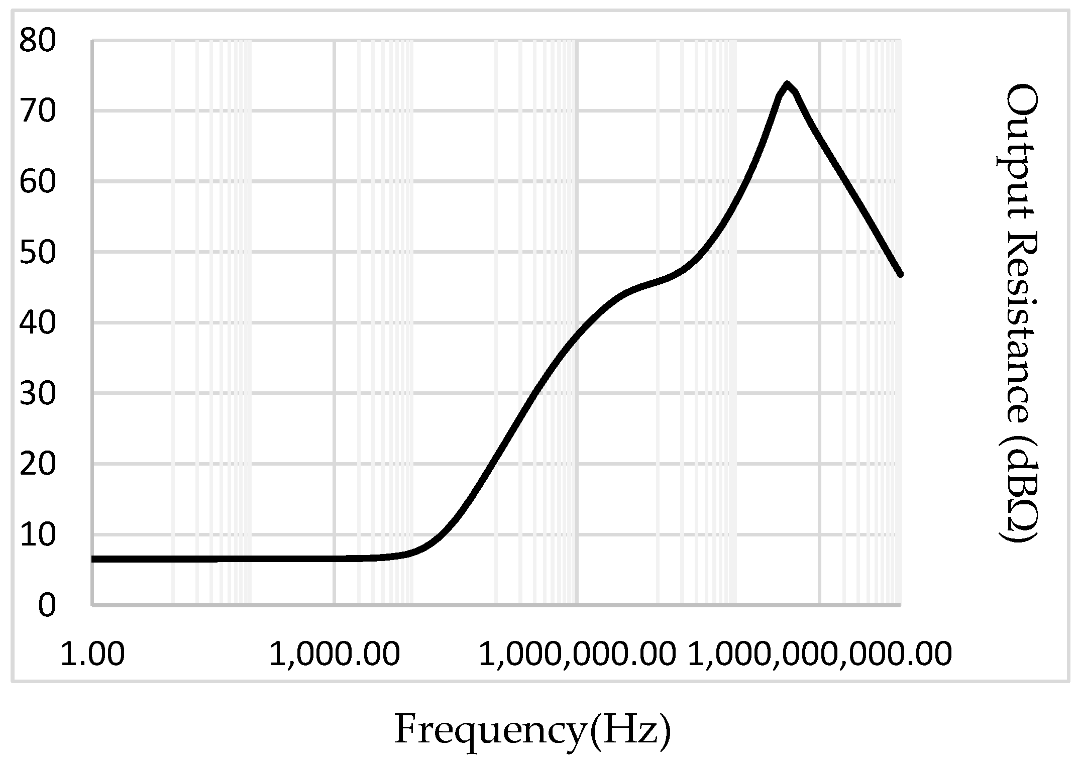
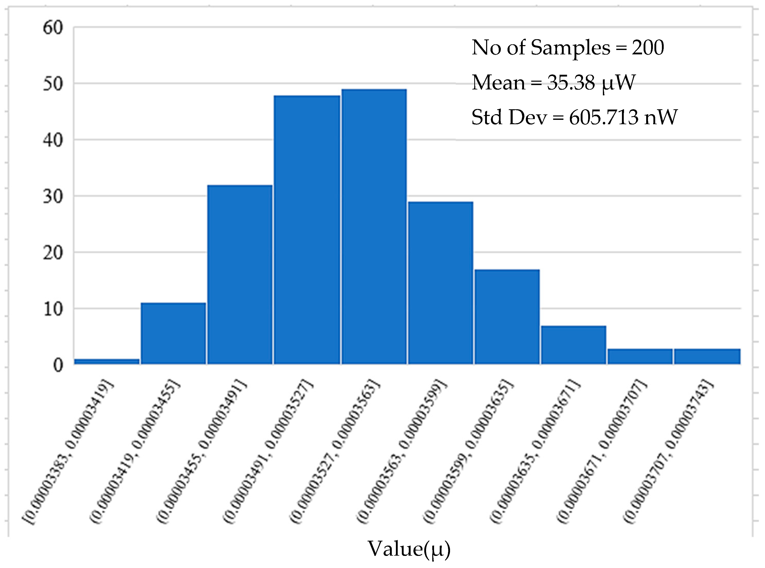
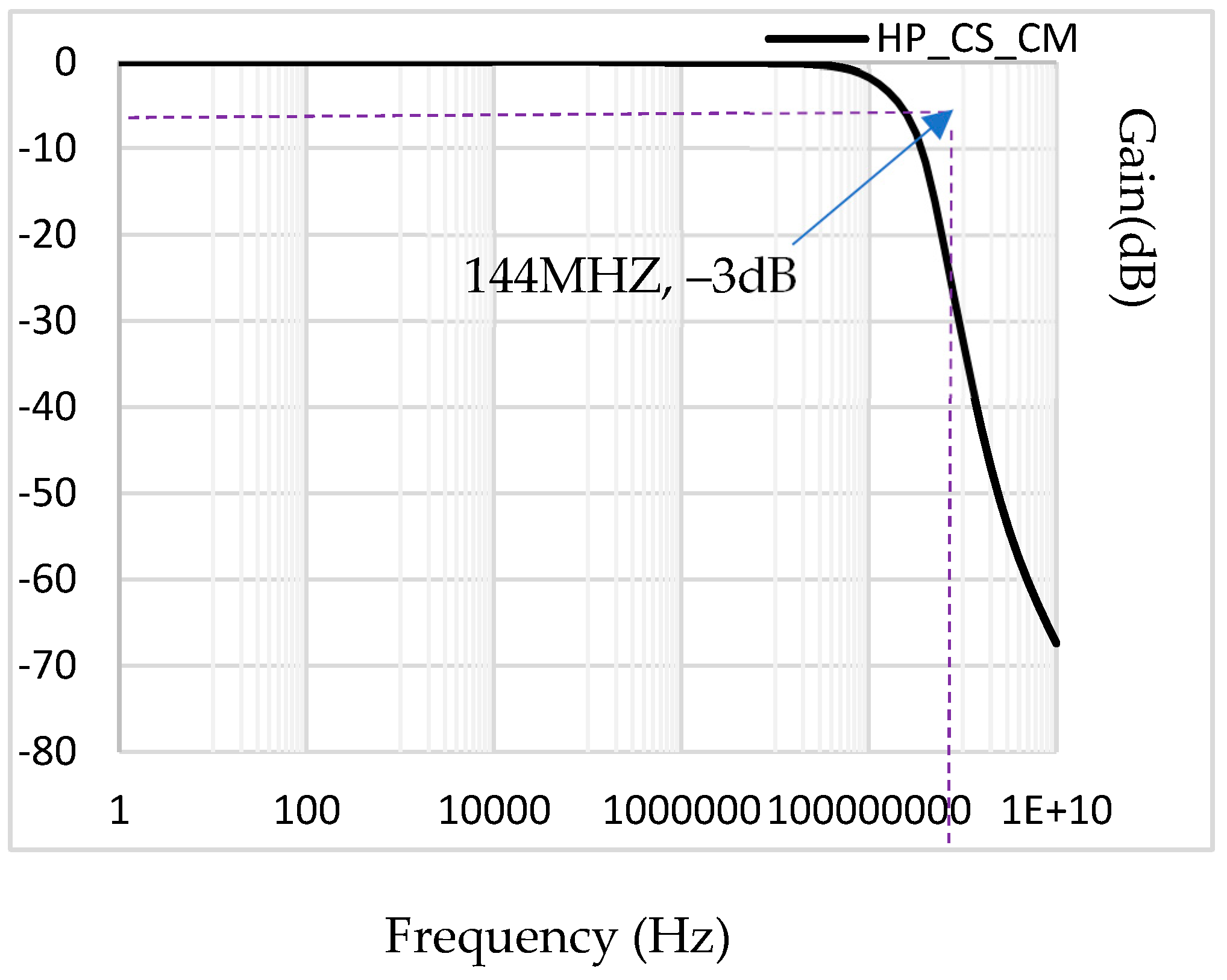
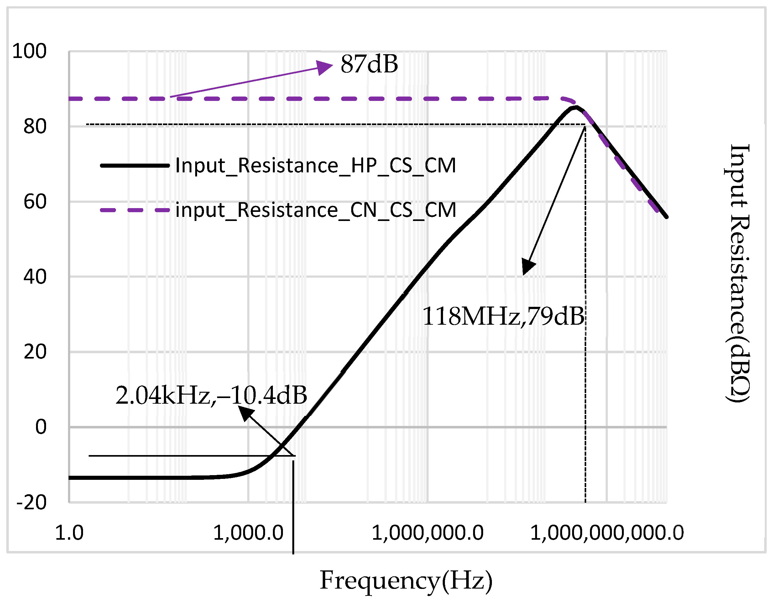
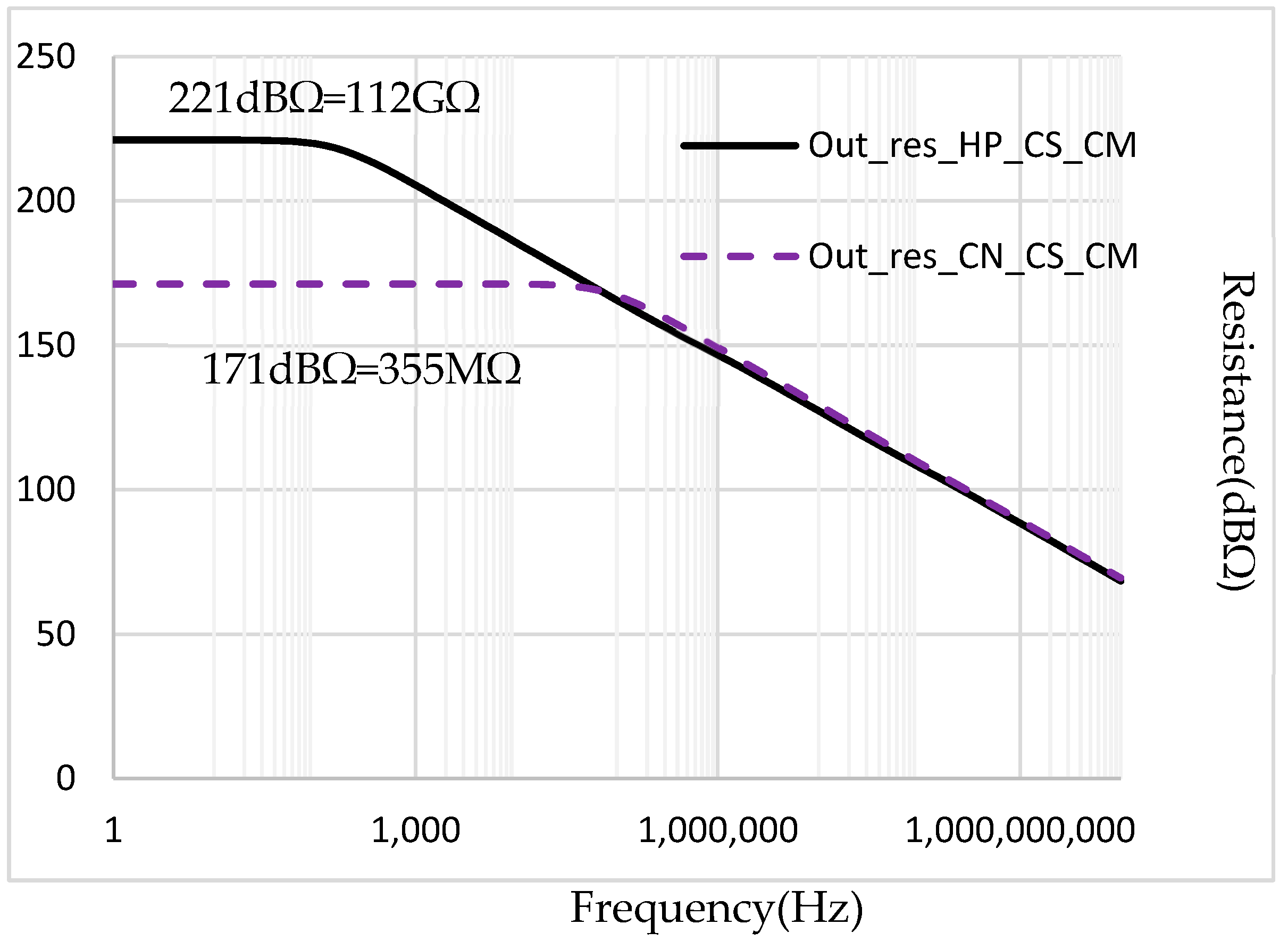
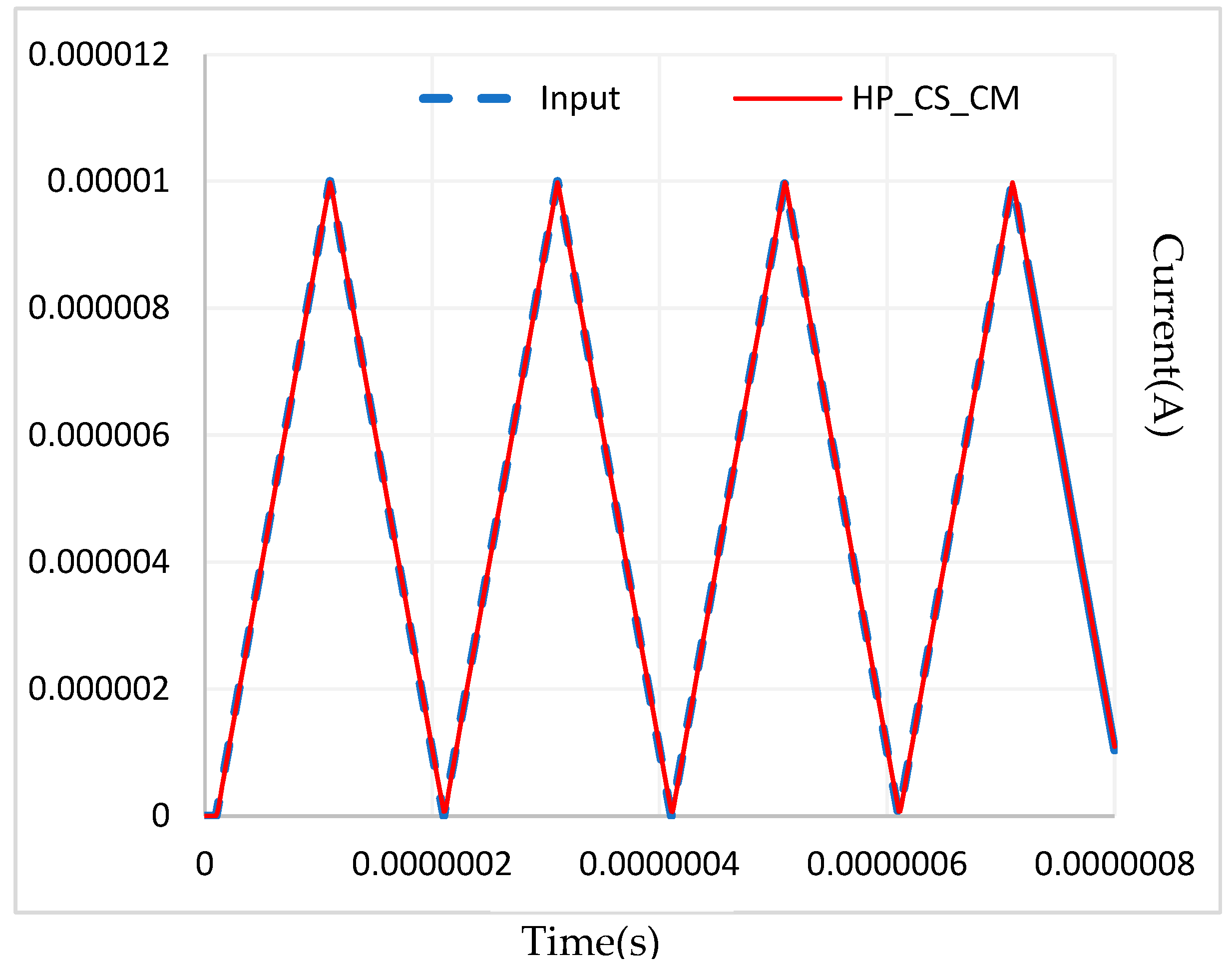
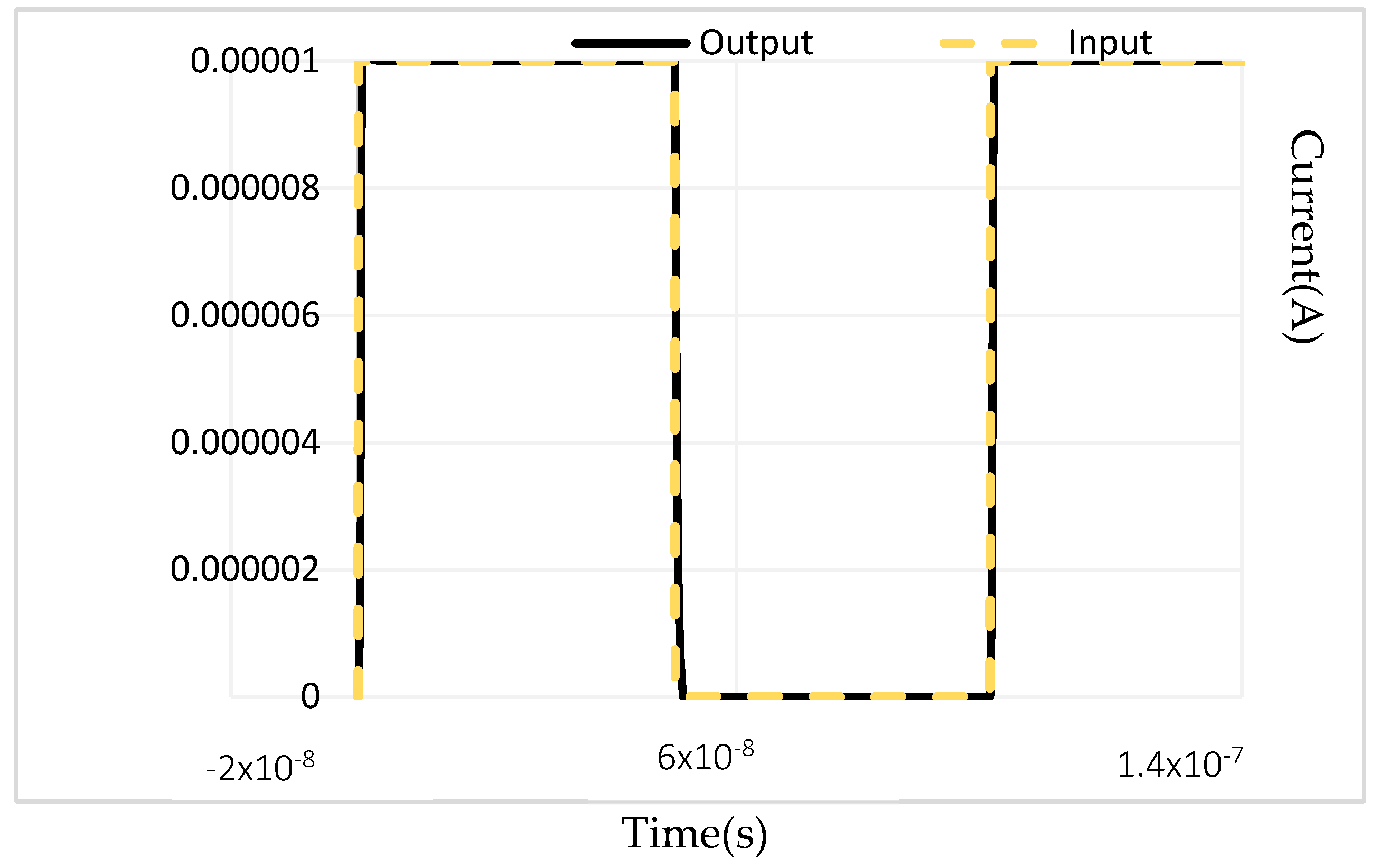
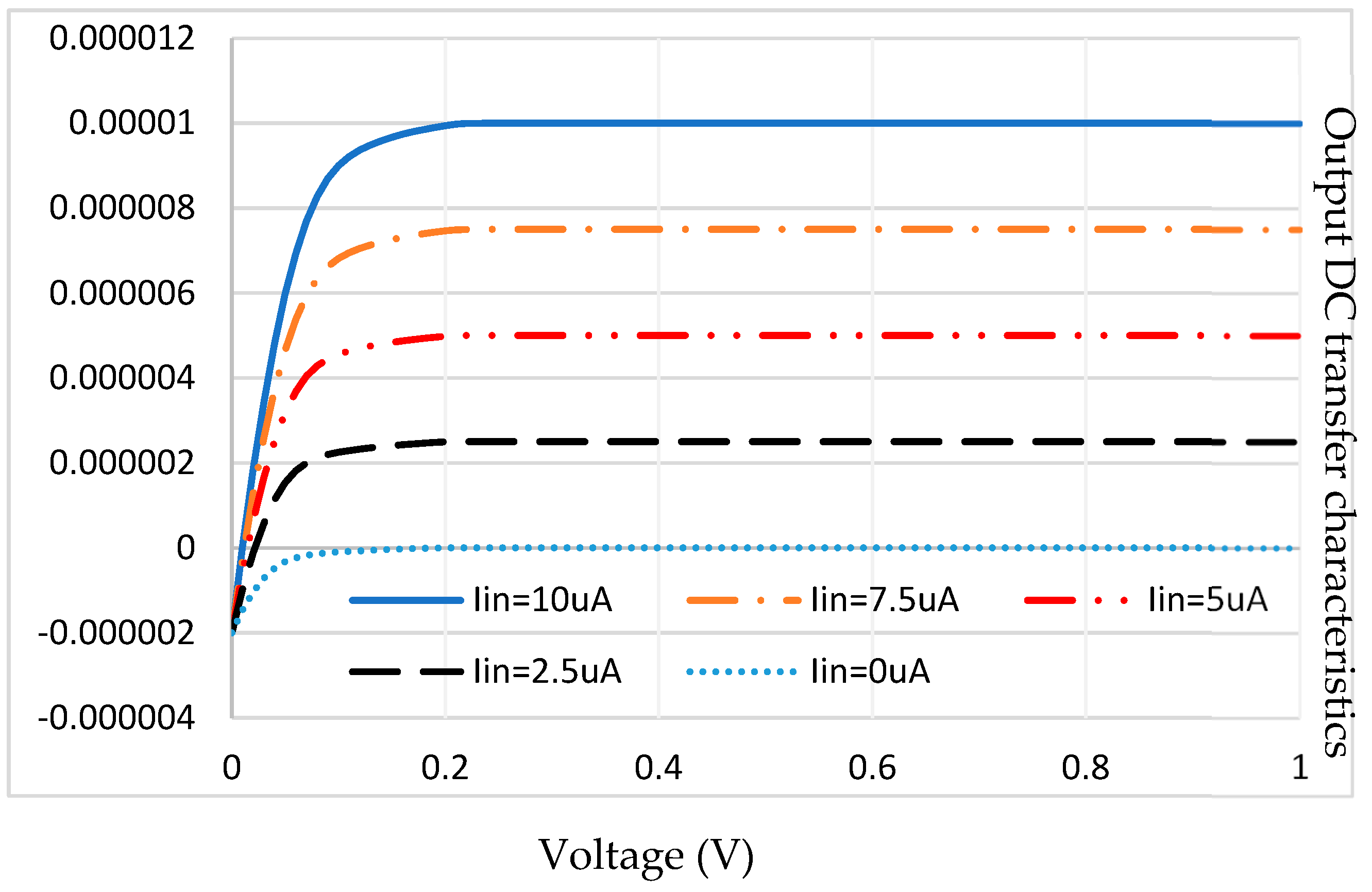
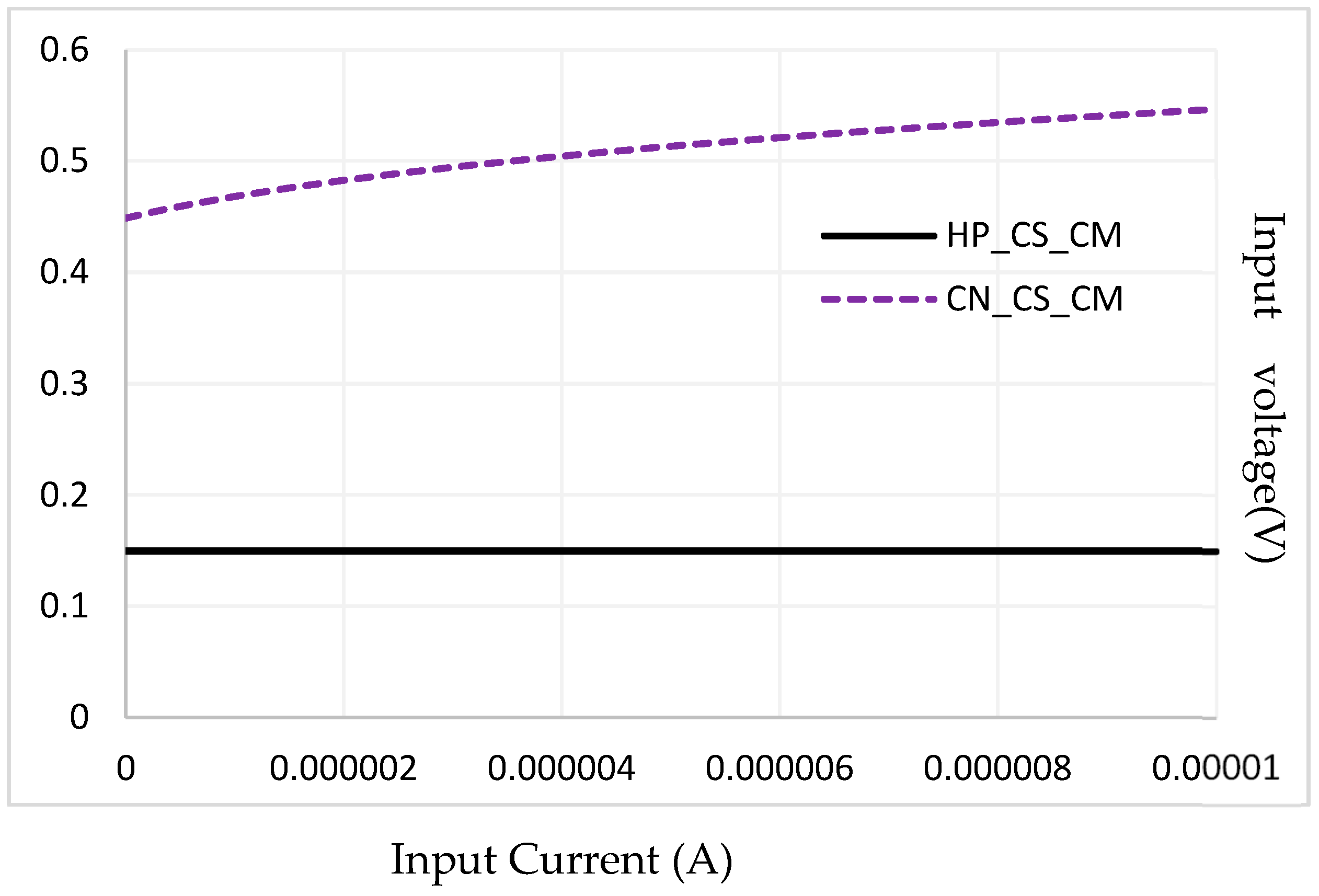
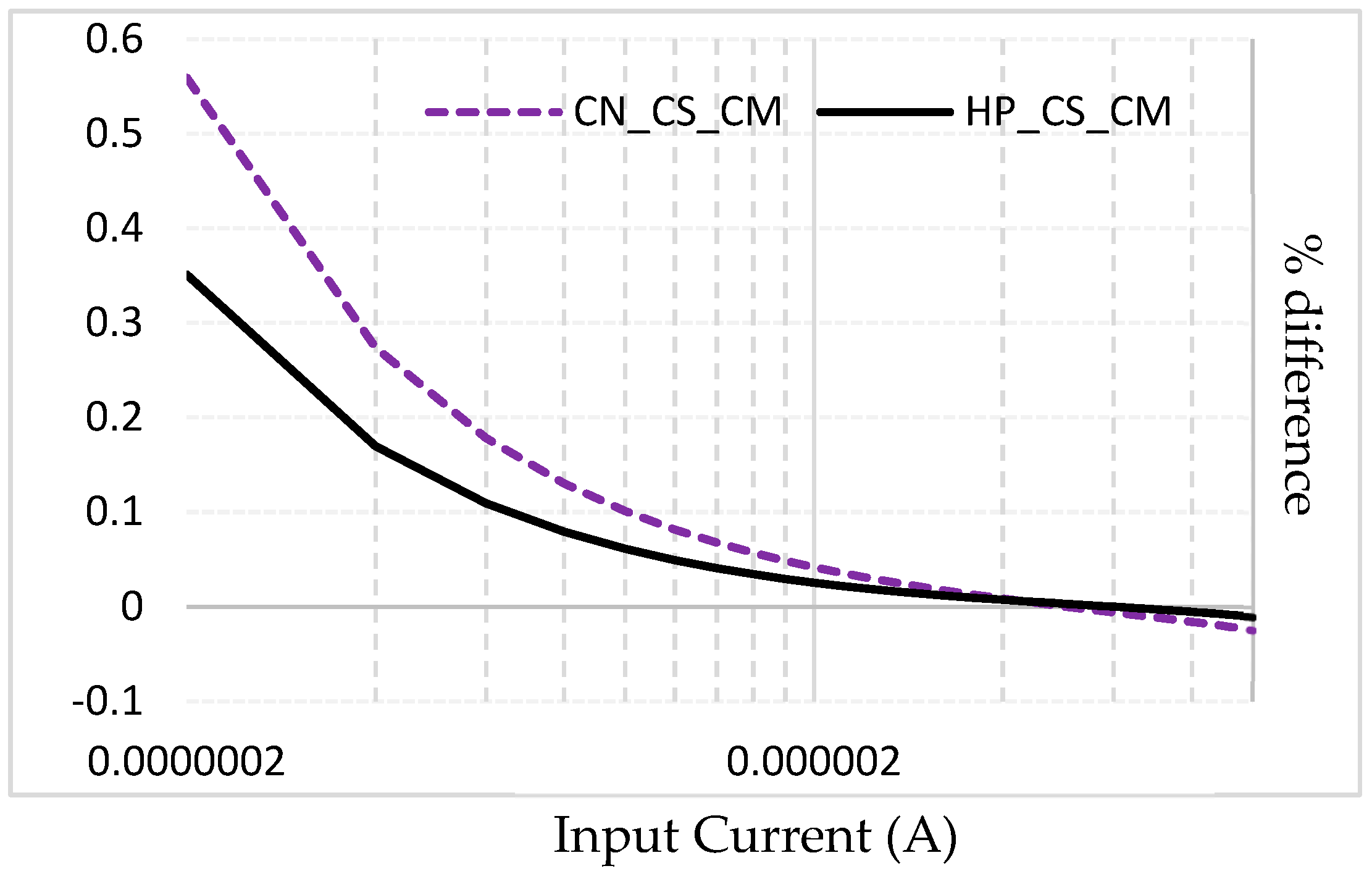
3.2. Simulation Results for Low-Voltage High-Performance Current Mirror HP_CS_CM

The CN_CS_CM and proposed HP_CS_CM current-mirror circuits of Figure 2a and Figure 4 were simulated in a commercial 180 nm CMOS technology with a supply voltage of 1V and Ibias = 2 µA. The resistor used to implement Rbat in the FVF level shifter has a value 75 kΩ. It is implemented using a PMOS transistor. The W/L ratio of the PMOS and NMOS transistors used in the input and output stages of both current mirrors are W/L = 5 µm/0.4 µm. Transistors used in the auxiliary amplifiers and the FVF level shifter of the proposed current mirror are scaled down by factor k = 10. This was performed in order to reduce the quiescent power dissipation. The compensation elements had values Cc = 1.5 pF and Rc = 4 kΩ.
Figure 11 shows the frequency response of the proposed high-performance cascoded current mirror (HP_CS_CM). It has a 144 MHz bandwidth. Figure 12 shows the frequency response of the input impedance of the conventional cascode mirror CN_CS_CM and of the proposed HP_CS_CM. The CN_CS_CM has constant input impedance of 22 kΩ, whereas the input impedance of the proposed current mirror is 0.212 Ω up to 800 Hz and 8.9 kΩ at 118 MHz. The HP_CS_CM has an input impedance, at low frequencies, that is close to 105 times lower than the CN_CS_CM.
Figure 13 shows the frequency response of the output impedance of the CN_CS_CM and of the HP_CS_CM. The proposed HP_CS_CM has an output impedance of 112 GΩ until 100 Hz, and the lowest output impedance is 18 MΩ through its bandwidth. On the contrary, the output impedance for the CN_CS_CM is 355 MΩ. Thus, the proposed high-performance current mirror has an output impedance that is 315 times higher than the CN_CS_CM at low frequencies.
Figure 14 shows the transient response to a triangular input current waveform. It can be seen that the proposed HP_CS_CM closely follows the linear input triangular current waveform. Figure 15 shows the transient pulse response of the proposed HP_CS_CM to a 10 MHz, 10 µA input pulse. It can be seen that the proposed HP_CS_CM has no peaking in the output pulse response.
An ideal current source is a circuit element that maintains a constant current flow independent of the voltage developed across its terminals as this voltage is determined by other circuit elements. To verify this property, Figure 16 shows the DC output transfer characteristics for dc voltage variation of 0 to 1 V by stepping the input current up from 0 to 10 µA in steps of 2.5 µA. It can be seen that the mirror compliance (minimum output) voltage for performance as a current source is approximately 0.2 V.
Figure 17 shows the input voltage of the CN_CS_CM and of the proposed HP_CS_CM by sweeping the input current Iin from o to 10 µA. It can be seen that the proposed HP_CS_CM has a constant 0.15 V input voltage, while the input voltage of the conventional mirror CN_CS_CM varies from 450 mV to 550 mV.
Figure 18 shows the gain error (in percent) e = 100[(Iout − Iin)/Iin] in the current transfer characteristic of the CN_CS_CM and the proposed HP_CS_CM as a function of the input current. It can be seen that, as expected, errors are similar since, in both mirrors, the drain-source voltages of input and output transistors are very similar. The total harmonic distortion of the proposed HP_CS_CM is given in Table 3 for a 200 µA amplitude sine wave at frequencies 500 Hz, 10 KHz, 1 MHz, and 100 MHz.
A Monte Carlo analysis with 200 samples was executed for some important parameters of the proposed HP_CS_CM for a 2 µA bias current. Table 4 gives the mean value and standard deviation of the bandwidth, input, output resistance, quiescent power, and gain for 200 runs. It can be see that the proposed current mirror is robust against process variation and mismatch effects. A noise analysis was also performed for the HP_CS_CM. The input referred noise was 14.5 pA/√Hz.
Table 5 compares the performance characteristics of the proposed HP_CS_CM to other low-voltage mirrors in the literature [17,18,19,20]. The proposed mirror has the highest output resistance and the lowest input resistance of all mirrors. Bandwidth is dependent on power dissipation. A mirror figure of merit FOMCM = BW/Pdiss is used to compare the circuits. Notice that the proposed mirror has the highest FOMCM in the table (the input compliance voltage of the resistance based mirror in [18] is lower but it has the serious shortcoming that, with the reported 39.6 mV input voltage, it is subject in practice to very large random gain/linearity errors caused by mismatch in VDS due to random offset of input and output transistors in the control circuit).

4. Conclusions

Two high-performance circuits based on the flipped voltage follower were introduced: (1) One was a class AB high-performance cascode flipped voltage follower that uses an additional output branch with a PMOS current-sourcing transistor. Replica biasing techniques are used to bias the sourcing transistor with a small quiescent current independent of the supply voltage. Under dynamic conditions, the sourcing transistor can provide very large positive output currents, which are over a factor 100 larger than the total quiescent current of the proposed circuit. Simulations in a commercial 0.18 µm CMOS technology have shown that it has low supply voltage requirements, greatly enhanced bandwidth, approximately symmetrical and large slew rates, and the largest small signal and large signal figures of merit of all class AB voltage followers. (2) The other was a low-voltage high-performance current mirror with 0.15 V input and 0.2 V output compliance voltages, 1 V supply voltage, extremely high output resistance (112 GΩ), extremely low input resistance (0.212 Ω), and the highest figure of merit.
This high-performance current mirror is implemented by utilizing two auxiliary amplifiers and a level shifter that boost the gain of the mirror cascode transistors and that equalize the drain source voltages of input and output mirror transistors. The auxiliary circuit increases the power dissipation of the mirror by only 25%. These characteristics were also verified with simulations in a commercial 0.18 µm CMOS technology.

Author Contributions

Conceptualization, J.R.-A., A.P, M.G., J.M.H.-M. and J.H.-C.; methodology, J.R.-A., A.P., M.G., J.M.H.-M. and J.H.-C.; validation, J.R.-A., A.P., M.G., J.M.H.-M. and J.H.-C.; formal analysis, J.R.-A., A.P., M.G. and J.H.-C.; investigation, J.R.-A., A.P., M.G. and J.H.-C.; resources, J.R.-A., A.P., M.G., J.M.H.-M. and J.H.-C.; data curation, J.R.-A., A.P., M.G., J.M.H.-M. and J.H.-C.; writing—original draft preparation, J.R.-A., A.P., M.G. and J.H.-C.; writing—review and editing, J.R.-A., A.P., M.G., J.M.H.-M. and J.H.-C.; visualization, J.R.-A., A.P., M.G., J.M.H.-M. and J.H.-C.; supervision, J.R.-A., A.P., M.G., J.M.H.-M. and J.H.-C.; project administration, J.R.-A., A.P., M.G., J.M.H.-M. and J.H.-C. All authors have read and agreed to the published version of the manuscript.

Funding

This research received no external funding.

Data Availability Statement

Data is contained within the article.

Conflicts of Interest

The authors declare no conflict of interest.

References

  1. Razavi, B. Design of Analog CMOS Integrated Circuits; McGraw Hill: Boston, MA, USA, 2001. [Google Scholar]
  2. Filanovsky, I.M.; Järvenhaara, J.; Tchamov, N.T. Source follower: A misunderstood humble circuit. In Proceedings of the 2013 IEEE 56th International Midwest Symposium on Circuits and Systems (MWSCAS), Columbus, OH, USA, 4–7 August 2013; pp. 185–188. [Google Scholar]
  3. Allen, P.E.; Holberg, D.R. CMOS Analog Circuit Design, 2nd ed.; Oxford Univeristy Press: Oxford, UK, 2002; Volume 2. [Google Scholar]
  4. Carvajal, R.G.; Ramirez-Angulo, J.; Lopez-Martin, A.J.; Torralba, A.; Galan, J.A.G.; Carlosena, A.; Chavero, F.M. The flipped voltage follower: A useful cell for low-voltage low-power circuit design. IEEE Trans. Circuits Syst. I Regul. Pap. 2005, 52, 1276–1291. [Google Scholar] [CrossRef]
  5. Ramirez-Angulo, J.; Gupta, S.; Padilla, I.; Carvajal, R.G.; Torralba, A.; Jimenez, M.; Munoz, F. Comparison of conventional and new flipped voltage structures with increased input/output signal swing and current sourcing/sinking capabilities. In Proceedings of the 48th Midwest Symposium on Circuits and Systems, Cincinnati, OH, USA, 7–10 August 2005; Volume 1152, pp. 1151–1154. [Google Scholar]
  6. Sawigun, C.; Demosthenous, A.; Liu, X.; Serdijn, W.A. A Compact Rail-to-Rail Class-AB CMOS Buffer With Slew-Rate Enhancement. IEEE Trans. Circuits Syst. II Express Briefs 2012, 59, 486–490. [Google Scholar] [CrossRef]
  7. Centurelli, F.; Monsurrò, P.; Trifiletti, A. A class-AB flipped voltage follower output stage. In Proceedings of the 2011 20th European Conference on Circuit Theory and Design (ECCTD), Linkoping, Sweden, 29–31 August 2011; pp. 757–760. [Google Scholar]
  8. Jindal, C.; Pandey, R. High Slew-Rate and Very-Low Output Resistance Class-AB Flipped Voltage Follower Cell for Low-Voltage Low-Power Analog Circuits. Wirel. Pers. Commun. 2022, 123, 215–228. [Google Scholar] [CrossRef]
  9. Xing, G.; Lewis, S.H.; Viswanathan, T.R. Self-Biased Unity-Gain Buffers With Low Gain Error. IEEE Trans. Circuits Syst. II Express Briefs 2009, 56, 36–40. [Google Scholar] [CrossRef]
  10. Paul, A.; Ramírez-Angulo, J.; Torralba, A. Bandwidth-Enhanced High Current Efficiency Class-AB Buffer With Very Low Output Resistance. IEEE Trans. Circuits Syst. II Express Briefs 2018, 65, 1544–1548. [Google Scholar] [CrossRef]
  11. Garde, M.P.; Lopez-Martin, A.; Cruz, C.A.D.l.; Carvajal, R.G. Wide-Swing Class AB Regulated Cascode Current Mirror. In Proceedings of the 2020 IEEE International Symposium on Circuits and Systems (ISCAS), Virtual, 12–14 October 2020; pp. 1–4. [Google Scholar]
  12. Moaf, M.; Piri, M.; Amiri, P. Two High Slew Rate Buffers Based on Flipped Voltage Follower. Int. J. Electr. Eng. Inform. 2016, 8, 451–460. [Google Scholar] [CrossRef]
  13. Ocampo-Hidalgo, J.J.; Alducín-Castillo, J.; Vázquez-Álvarez, I.; Oliva-Moreno, L.N.; Molinar-Solís, J.E. A CMOS Low-Voltage Super Follower Using Quasi-Floating Gate Techniques. J. Circuits Syst. Comput. 2017, 27, 1850111. [Google Scholar] [CrossRef]
  14. Centurelli, F.; Monsurrò, P.; Ruscio, D.; Trifiletti, A. A new class-AB Flipped Voltage Follower using a common-gate auxiliary amplifier. In Proceedings of the 2016 MIXDES—23rd International Conference Mixed Design of Integrated Circuits and Systems, Lodz, Poland, 23–25 June 2016; pp. 143–146. [Google Scholar]
  15. Ocampo-Hidalgo, J.J.; Molinar-Solis, J.E.; Oliva-Moreno, N.; Ponce-Ponce, V.H.; Ramirez-Salinas, M.A. The Merged Voltage Follower: A Class-AB CMOS Follower with Enhanced Bandwidth to Drive Loads with Low Resistance and Large Capacitance Le suiveur de tension fusionné: Un suiveur CMOS de classe AB avec une bande passante améliorée pour piloter des charges avec une faible résistance et une grande capacité. IEEE Can. J. Electr. Comput. Eng. 2021, 44, 30–40. [Google Scholar] [CrossRef]
  16. Jindal, C.; Pandey, R. Class-AB level shifted flipped voltage follower cell using bulk-driven technique. IET Circuits Devices Syst. 2018, 12, 286–294. [Google Scholar] [CrossRef]
  17. Aggarwal, B.; Gupta, M.; Gupta, A.K.; Sangal, A. A new low voltage level-shifted FVF current mirror with enhanced bandwidth and output resistance. Int. J. Electron. 2016, 103, 1759–1775. [Google Scholar] [CrossRef]
  18. Safari, L.; Minaei, S. A Low-Voltage Low-Power Resistor-Based Current Mirror and Its Applications. J. Circuits Syst. Comput. 2017, 26, 1750180. [Google Scholar] [CrossRef]
  19. Doreyatim, M.; Akbari, M.; Nazari, M.; Mahani, S. A low-voltage gain boosting-based current mirror with high input/output dynamic range. Microelectron. J. 2019, 90, 88–95. [Google Scholar] [CrossRef]
  20. Bchir, M.; Aloui, I.; Hassen, N. A bulk-driven quasi-floating gate FVF current mirror for low voltage, low power applications. Integration 2020, 74, 45–54. [Google Scholar] [CrossRef]
Figure 1. (a) Conventional voltage follower, (b) basic FVF, and (c) cascode FVF.
Jlpea 13 00028 g001
Figure 2. (a) Conventional cascode current mirror and (b) FVF-based low-voltage cascode current mirror with reduced input impedance.
Jlpea 13 00028 g002
Figure 3. High-performance class AB cascode FVF.
Jlpea 13 00028 g003
Figure 4. (a) Scheme of the proposed low-voltage high-performance current mirror, (b) transistor level implementation and biasing circuit, and (c) implementation of resistor R, cascode current source I*bias and simple current sources Ibias.
Jlpea 13 00028 g004
Figure 5. Frequency Response of the proposed HP_CSCFVF, CONV_VF, CONV_FVF and CONV_CSCFVF.
Jlpea 13 00028 g005
Figure 6. (a) Pulse response of the proposed HP_CSCFVF and CONV_CSCFVF for CL = 100 pF and (b) output current of the HP_CSCFVF and CON_CSCFVF at CL = 100 pF.
Jlpea 13 00028 g006
Figure 7. Pulse response of proposed HP_CSCFVF for load capacitor values: 10 pF, 32 pF, 55 pF, 77.5 pF and 100 pF.
Jlpea 13 00028 g007
Figure 8. Output resistance variation with frequency of the proposed HP_CSCFVF.
Jlpea 13 00028 g008
Figure 9. Layout of the proposed HP_CSCFVF.
Jlpea 13 00028 g009
Figure 10. Monte Carlo analysis of the Proposed HP_CSCFVF quiescent power dissipation over 200 samples MC simulation for process and mismatch variation.
Jlpea 13 00028 g010
Figure 11. Frequency response of the High performance cascode current Mirror.
Jlpea 13 00028 g011
Figure 12. Variation of input resistance with the frequency of Proposed HP_CS_CM and CN_CS_CM.
Jlpea 13 00028 g012
Figure 13. Variation of output resistance with frequency of High Performance HP_CS_CM and CN_CS_CM.
Jlpea 13 00028 g013
Figure 14. Transient response of the High performance Current Mirror.
Jlpea 13 00028 g014
Figure 15. Transient Pulse Response of High-Performance Current Mirror.
Jlpea 13 00028 g015
Figure 16. Output DC transfer characteristics of HP_CS_CM Voutmin = 0.2 V.
Jlpea 13 00028 g016
Figure 17. Input voltage with variation of input current.
Jlpea 13 00028 g017
Figure 18. Error in current transfer characteristic of the CN_CS_CM and HP_CS_CM.
Jlpea 13 00028 g018
Table 1. (A) Corner analysis at 27 °C; (B) corner analysis at 120 °C; (C) corner analysis at −20 °C.
(A)
CornerttfffssfssSD
ITotQ (µA)21222122210.49
f3dB (MHZ)14.61815.214.512.51.77
SR (V/µs)24.32821.525.621.72.4
Ioutpk (mA)2.683.042.52.72.420.2
(B)
CornerttfffssfssSD
ITotQ (µA)26292627251.35
f3dB (MHZ)1518.515.214.812.71.86
SR (V/µs)22.525.520.1822.3420.131.9
Ioutpk (mA)2.452.732.382.422.220.16
(C)
CornerttfffssfssSD
ITotQ (µA)20202019190.49
f3dB (MHZ)14.417.615.814.812.31.74
SR (V/µs)26.629.322.925.822.82.4
Ioutpk (mA)2.793.062.672.82.50.18
Table 2. Comparison of the proposed HP_CSCVF with state-of-the-art work.
ParameterRef./Year
[6]/2012
Ref./Year
[12]/2016
Ref./Year
[13]/2018
Ref./Year
[14]/2016
Ref./Year
[15]/2021
Ref./Year [16]/2018CONV_VF
Figure 1a
This Work
Figure 3
Process technology (µm)0.350.180.180.50.0450.50.180.180.18
ExpSim by Auth.SimExpSimExpSimSimSim
Supply (V)3±0.91.21.51.221.2±0.75±0.75
ITotQ (µA)8124320.8808.36920921
Load Cap. (pF)205010/100501471100100
BW (MHz)5.83.6515@100 pF1017032670.20.34714.6
Ioutpk+ (mA)1.623.160.321.80.171.590.1160.0852.6
Ioutpk− (mA)1.673.16NA1.80.081.420.1200.0342.47
SR+ (V/µS)79.463.232@10 pF364233.8116.62.534.47
SR (V/µS)83.663.2NA365030.3120.51234.03
Output resistance
(Ω)
NANA56NA1.15kNA1441.2k2.11
Quiescent power PdissQ (µWatt)24343725120101382413.531.5
FOMCE =
Ioutpk/ITotQ
20121522.510205.83.7118
FOMSS =
BWxCL/PdissQ
[(MHz)pF]/µW
0.470.42604.161710.9282.546
FOMGlobal3.062.24309.7131512.73.0473
Table 3. Variation in THD with frequency for HP_CS_CM at different frequencies with 200 µA amplitude sinusoidal current.
Frequency (Hz)THD (dB)
500−60
10 k−62
1 M−60
100 M−40
Table 4. Summary of results of 200 samples Monte Carlo analysis of proposed current mirror’s parameter.
Parameter NameMean ValueStandard Deviation
Bandwidth (MHz)1440.789
Input resistance (dBΩ)−13.70.728
Output Resistance(dBΩ)2210.505
Quiescent Power (µW)5.330.066
Gain (A/A)0.99917.8 µ
Table 5. Comparison of the proposed HP_CS_CM with state-of-the-art work.
Parameter[17][18][19][20]This Work
Input
Compliance Voltage
520 m39.6 m --150 m
Current
Transfer error (%)
1.710.60.160.220.1
Input resistance (Ω)21.4349668.31300.212
Output
Resistance (Ω)
1.14 G1 M10.5 G9.5 G112 G
Bandwidth (Hz)6.17 G181 M402 M2.7 G144 M
Noise (pA/√Hz)--7.8--
Supply (V)10.9111
Power (µW)916.65154110142.95
FOMCM (MHZ/µW)6.731.173.618.8928.8
Technology (µm)0.180.180.180.180.18
Disclaimer/Publisher’s Note: The statements, opinions and data contained in all publications are solely those of the individual author(s) and contributor(s) and not of MDPI and/or the editor(s). MDPI and/or the editor(s) disclaim responsibility for any injury to people or property resulting from any ideas, methods, instructions or products referred to in the content.

