1. Introduction
The Internet of things (IoT) is heavily driven by significant semiconductor and nanotechnology breakthroughs. Low-cost, reliable, and highly integrated circuits and systems have been designed, allowing for the introduction of important features such as remote access control and the operation of large amounts of data [
1].
High-resolution analog-to-digital (A/D) converters (ADCs) are relevant building blocks in different IoT systems. Applications such as high-precision sensor networks, communications, imaging, and signal processing require outstanding ADC performance, including high-accuracy, low-power consumption, and, in some cases, wide-bandwidth (BW) specifications [
2].
To accomplish a high resolution, delta-sigma (
) modulators (
M) and successive approximation register (SAR) ADCs (SAR-ADCs) are frequently utilized. While in
M, larger sampling frequencies (
) are used to achieve higher resolutions, in conventional SAR-ADCs, energy efficiency is often sacrificed to reach the target resolution. Furthermore, old-fashioned architectures and techniques were revisited, and hybrid structures are currently a reality, mixing these schemes with popular structures. Employing noise shaping (NS) in an SAR-ADC and using a delta modulation in a
M, resulting in a delta-delta-sigma (
) modulator (
M), are examples of this new era of hybrid ADC architectures pursuing the most outstanding and efficient ADC [
3,
4,
5].
Taking into consideration that the ADC design is a complex and time-consuming task, it is desirable to reduce this effort, especially when porting between different nodes or technologies is required. Moreover, the lower nodes’ technology constraints (low intrinsic gain, reduced supply voltage, leakage current, etc.) bring other challenges in porting tasks, sometimes requiring a complete redesign or the implementation of different circuit schemes.
Circuits based on digital logic can be quickly realized and modified to accomplish specifications and technological changes. Therefore, the use of digital circuits is becoming popular in analog or mixed-signal circuit design, such as in the case of ADCs. Consequently, synthesizable solutions using standard cells are used to further reduce redesign time and effort [
6,
7,
8].
In this work, the most-suited ADC architectures for IoT applications are described. A hybrid ADC solution, a digital–delta (Δ) modulator (ΔM) with NS, is proposed that can be implemented using only passive and digital circuitry based on standard cells. Circuit details and some simulation results are also provided.
This paper is organized as follows.
Section 2 presents the most popular ADC architectures for IoT applications, where complexity, dynamic performance, and energy efficiency are compared. In
Section 3, some standard-cell-based active building blocks, comparators, and integrators, are presented with reference to their advantages and the main challenges during their integration in complex systems.
Section 4 provides schematic details regarding the proposed standard-cell-based digital-ΔM employing NS and some simulation results. Lastly, the main conclusions are drawn in
Section 5.
2. Most-Suited Analog-to-Digital Converter (ADC) Architectures for Internet of Things (IoT)
The most suited ADC architectures for IoT applications are described in this section. In spite of being an old-fashioned topology and not directly implemented in IoT applications, ΔM is mentioned because it is the basis of M and has inspired some other hybrid architectures, such as SAR-ADC with NS, M or the proposed digital-ΔM with NS ADCs.
Lastly, a qualitative comparison between them is provided considering complexity, dynamic performance, and energy efficiency.
2.1. Delta Modulator (ΔM) ADC
In a patent from 1946 submitted by Deloraine et al., delta modulation was referred to for the first time as a method to transmit analog data by means of a one-bit code [
9].
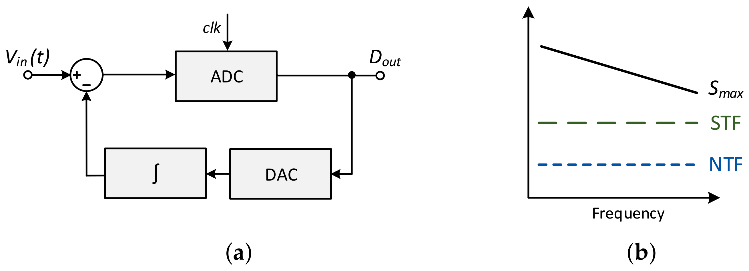
As shown in
Figure 1a, the basic ΔM transforms an analog input signal,
, into a synchronous digital output,
. It employs a 1-bit quantizer, a digital-to-analog (D/A) converter (DAC), and an integrator in the feedback path as an attempt to anticipate the input signal. Thus, this integrator acts as a predictor [
10].
Noise can negatively impact ΔM performance in two different ways: through granular noise or slope overload. While the former results from the quantization of a continuous signal (the signal is forced to assume a discrete value), the latter is dominant when the step size of the integrator is too small, resulting in the incorrect tracking of the input signal [
10,
11].
Despite the good robustness to transmission errors, simple filtering requirements, and low associated complexity, the nonidealities associated with the integrator in the feedback path can limit linearity, noise performance, and system accuracy. Furthermore, the amplitude of
and ADC performance are inversely proportional to the input signal frequency,
. Therefore, as
Figure 1b illustrates, while the signal transfer function (STF) and the noise transfer function (NTF) are constant, the maximal signal,
, decreases with the frequency [
5].
Both noise and nonidealities can be problematic and severely restrict the maximal dynamic performance of the converter [
4].
2.2. SAR-ADC with Noise Shaping (NS)
SAR-ADCs are currently one of the most popular topologies to realize A/D conversion due to their energy efficiency, low die area, and low circuit complexity [
12]. However, higher resolutions are difficult to achieve without sacrificing energy efficiency.
In conventional topologies, the circuit relies essentially on a 1-bit comparator, an
N-bit DAC, and a sample-and-hold (S/H) block. A binary-search algorithm is used to reduce the analog residue to less than one least significant bit (LSB) [
13].
Like in other architectures, the most critical building block is the DAC because its nonidealities, the associated noise, and its settling time dominated by the reference settling directly affect the ADC performance. This aspect is even more crucial for high-resolution converters.
In the last decade, the introduction of oversampling and NS in the conventional SAR-ADC allowed for better higher dynamic performance beyond 14 bits of resolution (i.e., 12.5 bits of effective number of bits (ENOB)) [
3]. The main idea is to use the analog residue that still remains after the SAR operation, the residue voltage (
), and integrate it to perform a NS, spreading the noise through a higher BW than the band of interest. The block diagram of a SAR-ADC employing NS is shown in
Figure 2a, in which the ADC can simply be a single comparator. In
Figure 2b, the STF, NTF, and
magnitudes as a function of frequency are illustrated, with the NTF slope characteristic from systems employing NS being notable.
Given the absence of amplifiers in the pure topology (besides the comparator), in these hybrid structures, the same strategy has been pursued, maintaining the circuit simplicity, and relaxing the specifications of the comparator and DAC [
14]. Thus, different works have been proposed using passive NS structures [
15,
16,
17].
2.3. First-Order Delta–Sigma () Modulator (M) ADC
The
M topology emerged to avoid the shortcomings of the ΔM by moving the integrator from the feedback to the forward path. As illustrated in
Figure 3a, in which the local quantizer (ADC) can again simply be a single comparator, the integrator operates over the error difference instead of the signal estimation, as in the ΔM case.
This architecture relies essentially on an analog filter (integrator), a quantizer, and a DAC [
4,
11]. Using the linear additive white-noise model for the quantizer, this system can be represented in the Z domain, resulting in the following STF and NTF:
where
is the integrator transfer function. The NS effect is more effective for higher
filter orders, promoting higher-resolution converters; however, extra complexity is added to the system. These functions are represented in
Figure 3b.
2.4. Delta–Delta–Sigma () Modulator (M) ADC
M is another example of a hybrid architecture. Combining delta modulation with a 1st-order
M,
M was proposed in [
5]. As depicted in
Figure 4a, two integrators are used in this topology, one in the feedforward and another in the feedback paths.
Since two integrators are involved, the complexity of the architecture is higher. Furthermore, the nonidealities of the DAC (placed in the feedback path) impact the ADC linearity. Thus, a high dynamic resolution is difficult to achieve, especially with low energy efficiency. Despite the inherent complexity, small modifications can be performed to the architecture, such as changing the relative position of the DAC and integrator in the feedback path. The integrator becomes a digital accumulator, reducing the complexity and rendering the architecture more suitable for IoT.
As represented in
Figure 4b, while the NS imposes an inclination to the NTF curve, shaping the noise for higher frequencies, delta modulation impacts the
(similarly to the ΔM topology).
2.5. Proposed Hybrid ADC: Digital–Delta (Δ) Modulator (ΔM) with Noise Shaping (NS)
A digital-ΔM employing NS was initially proposed by the authors of this paper in [
18]. It utilizes oversampling and NS to improve the overall performance by minimizing the impact of thermal and quantization noise. As depicted in
Figure 5, it comprises a 1-bit comparator, an accumulator, an
N-bit DAC, an S/H circuit, and an integrator in the NS section.
This architecture was initially inspired by an SAR-ADC. However, instead of the typical SAR logic, this topology uses an accumulator in the digital domain. Therefore, the search algorithm is based on the prediction of the next working as a ΔM.
Comparing the block diagram of the proposed ADC architecture, depicted in
Figure 6a, with other topologies shows that the comparator also connects to the sampled
to perform a direct comparison with the estimation. Additionally, this architecture employs an accumulator placed between the comparator and the DAC, which is a relevant advantage to achieve a fully synthesizable ADC. However, since this topology utilizes delta modulation,
is dependent on the frequency (
Figure 6b).
2.6. Comparison among the Most-Suited Architectures
All the described architectures are qualitatively compared in
Table 1.
In all the described topologies, the most critical building blocks are the comparator, integrator, and the DAC, since their nonidealities impact ADC performance. However, depending on the ADC architecture and the circuit location, their effect can be distinct.
Generally, SAR-ADC and digital-ΔM, both employing NS, present higher complexity when compared with M or M ADCs because the specifications of the main building blocks (metastability, comparator’s accuracy and comparison times, noise, etc.) have strong repercussions on ADC performance. However, they present very good energy efficiency, increasing their attractiveness. M or M ADCs are also popular for high-resolution applications. However, the integrator design can, in some cases, be problematic for circuit stability and efficiency.
The magnitude of
can show different behaviors depending on the architecture; therefore, despite the conclusions depicted in
Table 1, this aspect should be taken into account to ensure that it does not represent a strong limitation for the specific IoT application.
3. Standard-Cell-Based Active Building Blocks
The implementation of the different architectures presented earlier demands different specific circuits to implement the distinct functional blocks that each topology requires. Typically, integrator synthesis encompasses the design of OTAs, and quantizers involve comparator design. Among others, these are fundamental building blocks of converters.
Over the years, different standard-cell-based circuits, recurring to automated digital design flows and standard cells, have been proposed to implement these well-known analog functions, enabling faster design, and synthesis and layout automation based on standard cells.
Despite the importance of the DAC in all architectures, its design has preferably been passive, facilitating the converter porting between different nodes or technologies. Furthermore, the passive characteristics allow for good energy efficiency, which is extremely relevant for IoT applications. For these reasons, this building block is not described here.
3.1. Dynamic Comparators Using Standard Logic Circuitry
A fully synthesizable dynamic voltage comparator was proposed by Weaver et al. in [
19]. As depicted in
Figure 7, the circuit relies on a two cross-coupled 3-input digital NAND gates and, when two NANDs are connected, assuming that the common-mode voltage of the input signal is high enough to cut off the input
PMOS devices, an analog-input comparator is created. When the clock is low, the outputs are reset to the positive supply rail,
, and when the clock goes high, the outputs start to discharge through the
NMOS devices. Since the discharging rate is proportional to the input, once one of the outputs achieves a value below than the threshold voltage, the cross-coupled connection forces the outputs to assume the supply rail values. A static SR latch is also used to hold the output decision and it is buffered by an inverter to reduce the memory effect.
In spite of being suitable for an all-digital implementation, this circuit is sensitive to the input common-mode range. Consequently, the usage of this comparator is restricted to stochastic ADCs [
20].
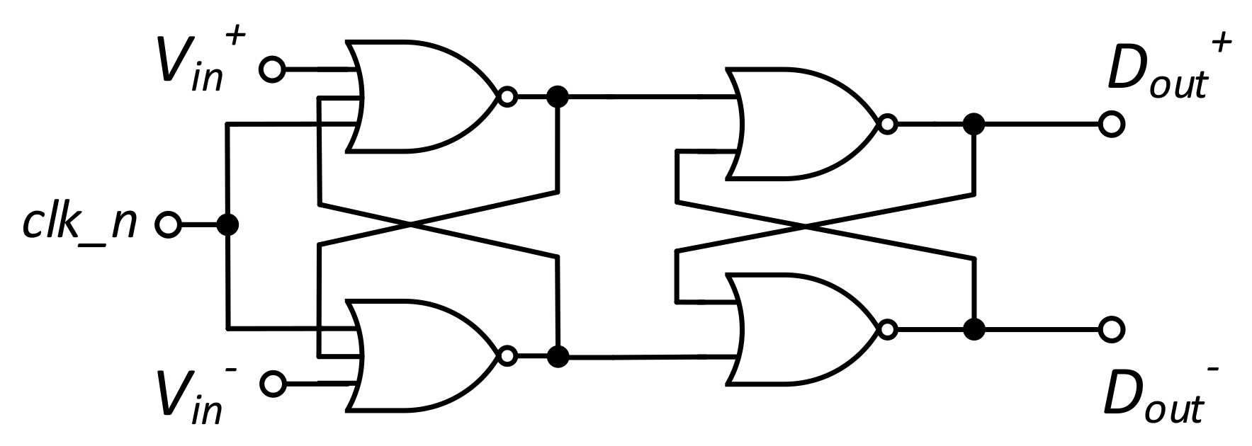
Replacing NAND gates with NOR gates, as shown in
Figure 8, the comparator only operates correctly if the input common-mode voltage is close to the ground. Thus, merging the 3-input NAND with 3-input NOR solutions, a rail-to-rail dynamic voltage comparator was proposed in [
20]. In this case, NAND gates operate correctly for the portion of the common-mode towards
, while NOR gates work properly for the portion towards the ground.
Ojima et al. proposed an NAND-based 4-input clocked comparator to achieve a fully synthesizable SAR ADC [
21]. As
Figure 9 shows, the four 3-input NAND gates define the preamplifier and the first latch stage (the output of one pair of preamplifiers is fed back to the input of the other pair), while the following 2-input NAND gates form the second latch stage, enhancing the comparator gain and reducing the comparison time. In this scheme, the comparison is carried out on the basis of (
+
) and (
+
).
In the previous scheme, when the
was low and the
clk was disabled, the reset path of the
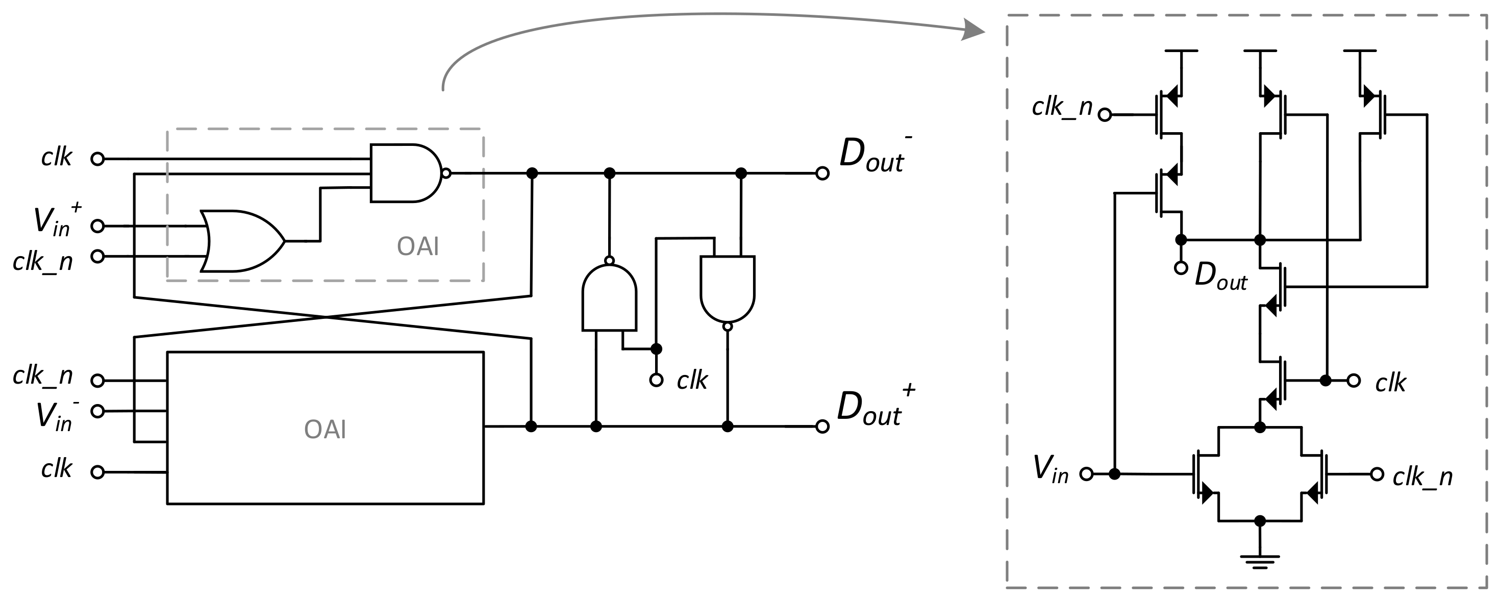
NMOS of the preamplifier was cut off. Consequently, a residue voltage remained at the drain node that could be amplified during the next comparison, generating an error output. To resolve that, it was proposed to replace the NAND gates with OR–AND inverter (OAI) cells [
6]. Thus, an explicit reset is performed on the drain nodes, eliminating the residue voltages and thereby reducing the probability of a wrong output.
On the basis of the described 4-input solution [
6], a 2-input comparator based on the same OAI cells was designed (
Figure 10). In addition to the obvious reduction in complexity and power dissipation, because fewer transistors are used, this topology presents satisfactory characteristics (comparison time, noise, and output error probability) for simple ADC topologies such as SAR-ADCs and digital-ΔM, both with NS.
Recently, different works have been proposed with the goal of achieving rail-to-rail dynamic voltage comparators with good energy efficiency [
22,
23].
3.2. Inverter-Based OTA Topologies
Amplifiers are also difficult to design and to port between technologies. Thus, standard-cell-based synthesizable solutions have been drawing attention in recent years. Inverter-based switched-capacitor (SC) circuits are one possibility that has been deeply studied due to the inherent simplicity and capability to operate with low , in contrast with other operational transconductance amplifiers (OTAs).
A simple inverter allows for a push–pull operation, a large output swing (OS), and good energy efficiency. Furthermore, both devices contribute to global transconductance [
24]. However, taking into consideration that the inverter does not have an explicit reference virtual ground, different cancellation techniques have been investigated to compensate the offset voltage,
, and reduce its impact [
25].
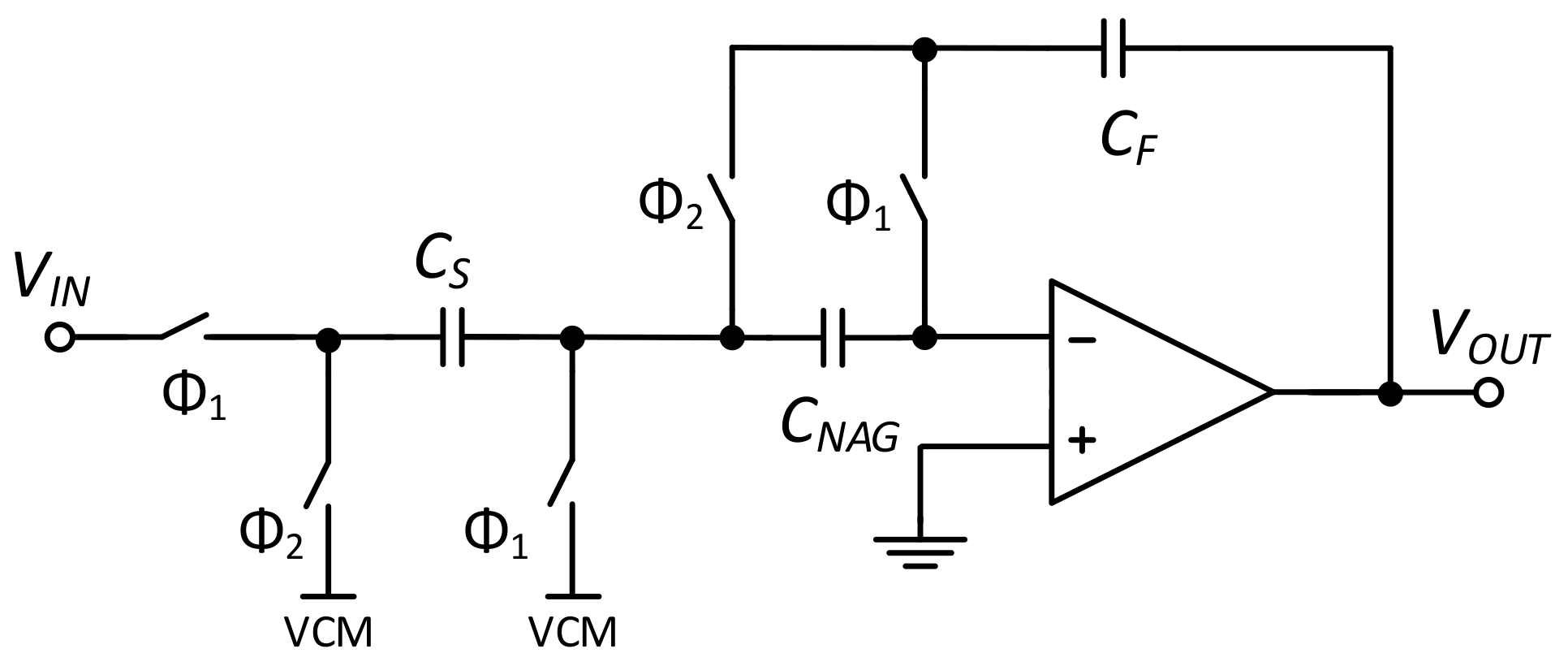
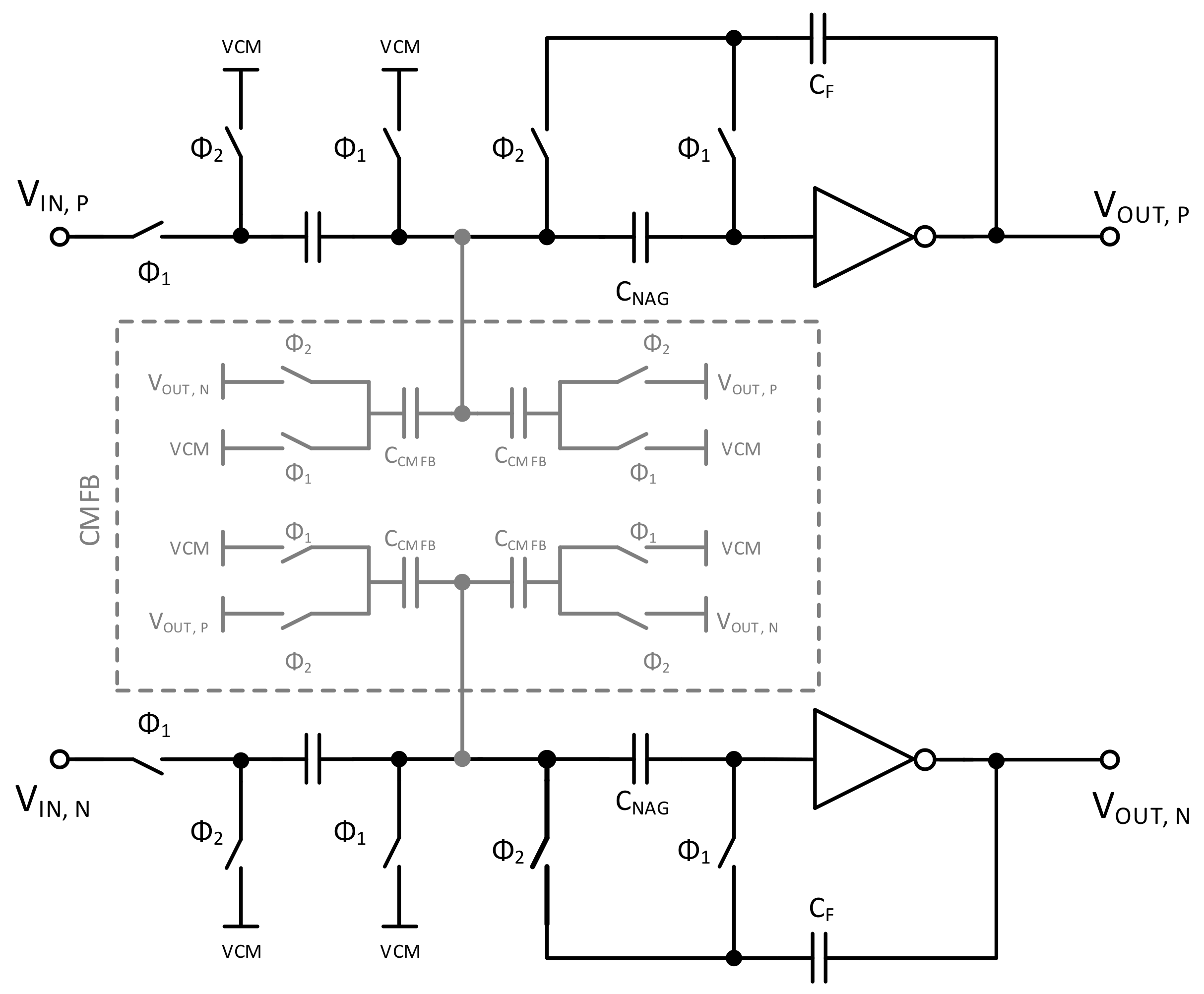
The technique proposed by Nagaraj et al. in [
26] is one of the most used approaches. Besides the offset impact reduction, it requires a lower gain specification, facilitating its design. In this scheme, depicted in
Figure 11, while capacitors
and
perform the integration, the
is used to compensate for the finite gain error and
[
25,
26,
27].
There are some relevant specifications with which OTAs need to comply in order to render them good candidates for employment in ADCs, namely, the gain and its linearity over , since it affects ADC linearity, low complexity, and good energy efficiency. These are fundamental requirements to be observed, especially for IoT and fully synthesizable applications.
Thus, the key performance parameters of three different OTA topologies were evaluated in [
28]. The circuits,
OTA 1,
OTA 2 and
OTA 3, can be described as follows:
OTA 1: a single pseudodifferential Nagaraj integrator with a fully passive SC common-mode feedback (CMFB) circuit, as illustrated in
Figure 12 [
24].
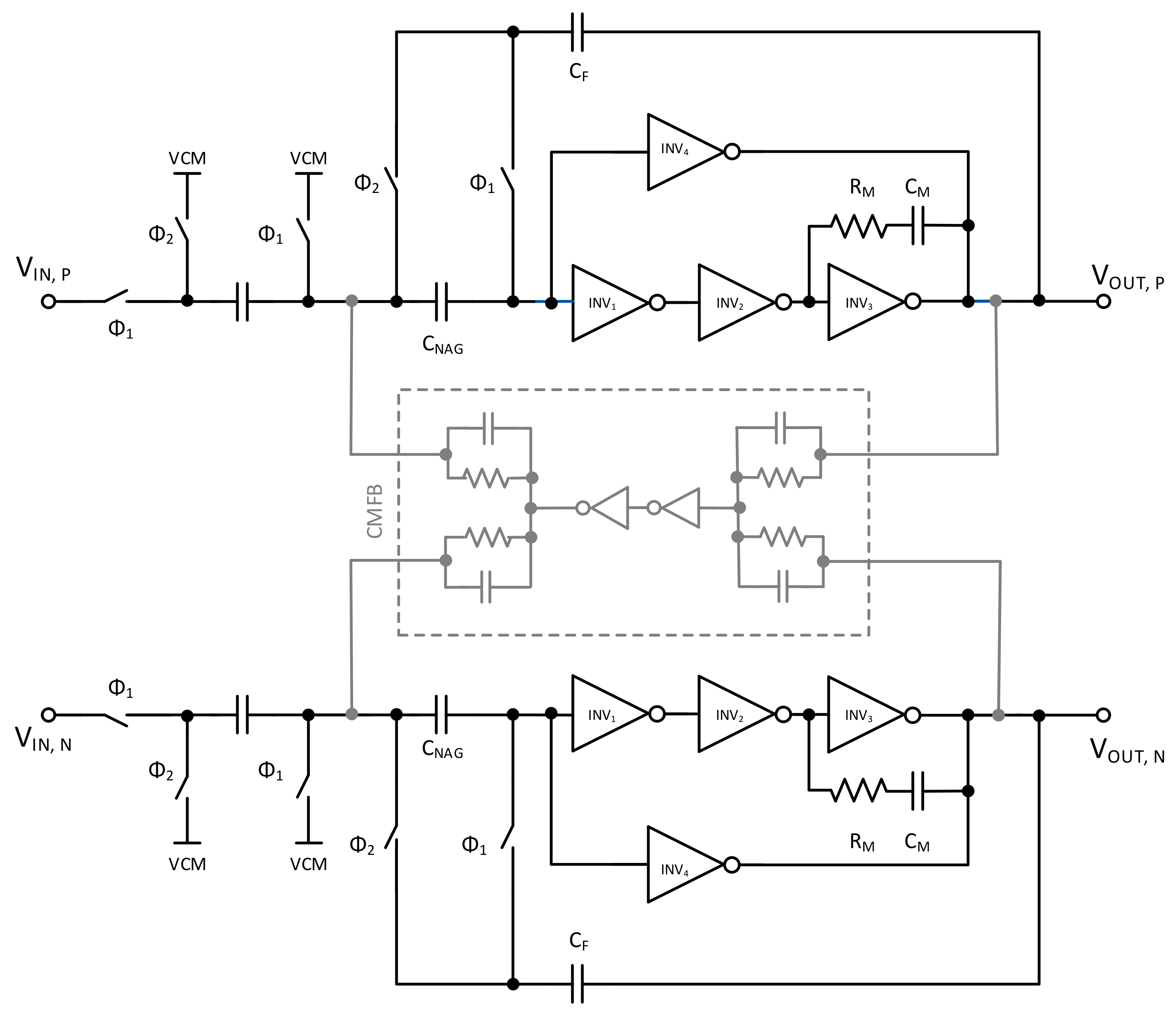
OTA 2: a pseudodifferential with a three-stage multipath inverter-based amplifier using a RC network as CMFB, as shown in
Figure 13 [
29].
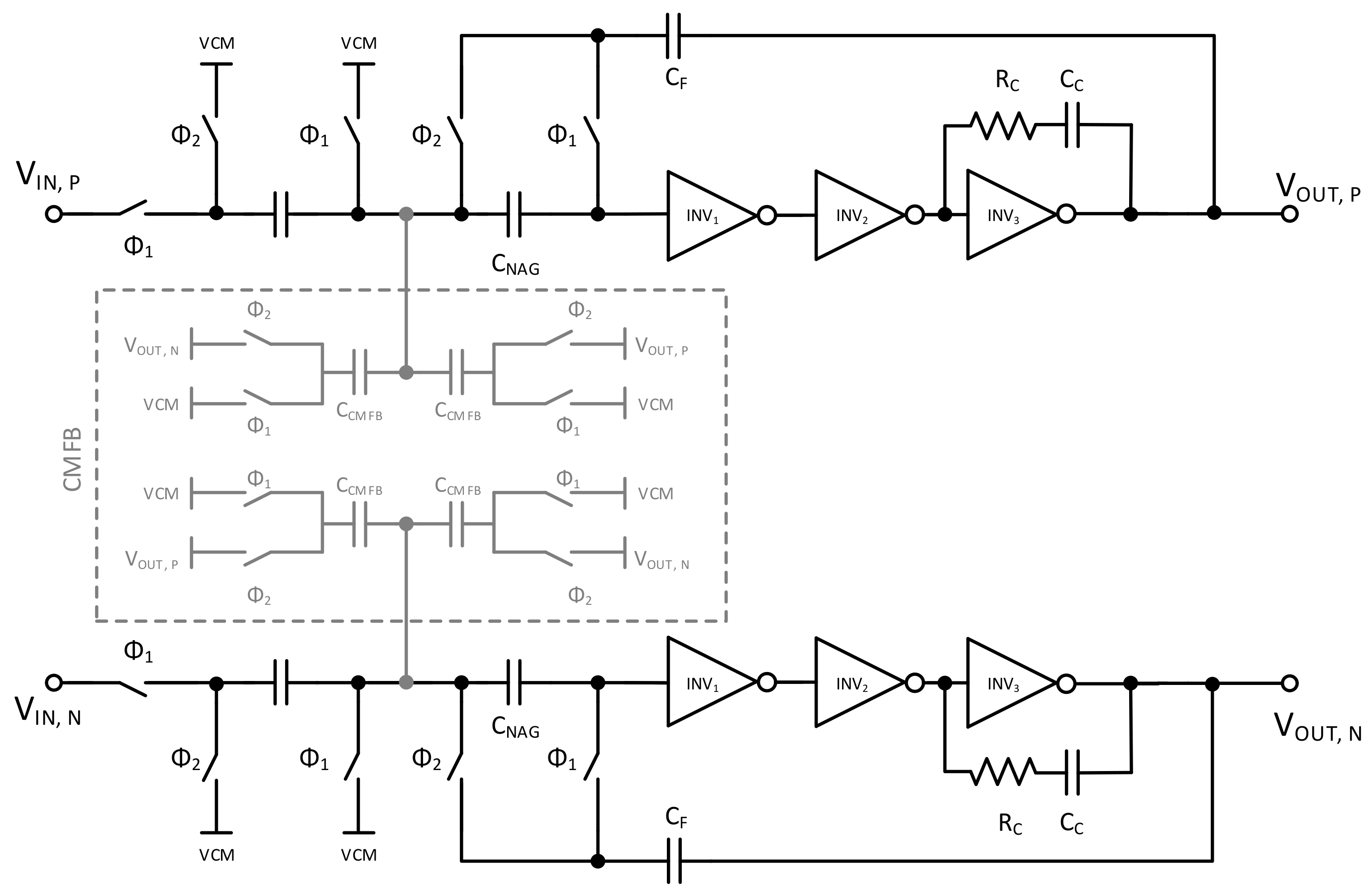
OTA 3: a single-path three-stage pseudodifferential Nagaraj integrator using a fully passive SC CMFB, as shown in
Figure 14.
As summarized in
Table 2, there are significant differences between these three OTA circuits. Since a cascade of inverters was used in
OTA 2 and
OTA 3, a higher DC gain was achieved. However, this also increased the complexity. Furthermore, the RC network utilized in
OTA 2 as CMFB increased the current consumption. Regarding the linearity over
, significant differences were also noticed with
OTA 2 and
OTA 3 being the best options when the linearity of the OTA is extremely important in the system, such as in the case of ADCs.
4. A Standard-Cell-Based Digital–Delta (Δ) Modulator (ΔM) with Noise Shaping (NS)
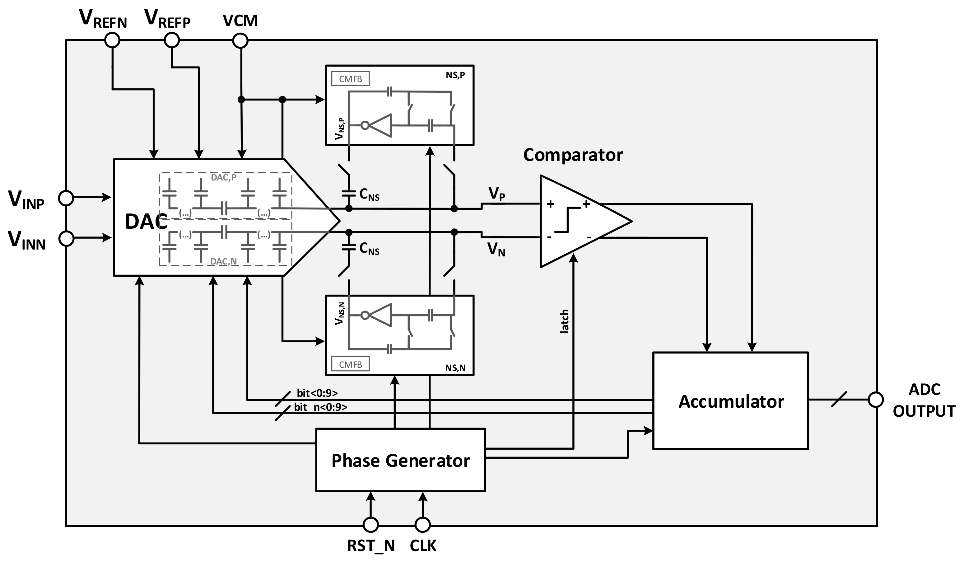
A complete and differential electrical scheme of the proposed ADC topology, a digital-ΔM employing NS, is depicted in
Figure 15, complementing the description in
Section 2.5. It comprises a split-capacitor DAC with embedded S/H, a pseudodifferential inverter-based Nagaraj integrator with a fully passive SC CMFB circuit (shown in
Figure 12), an OAI-based comparator (whose circuit is shown in
Figure 10), an accumulator, and a phase generator. Thus, a fully synthesizable ADC is demonstrated, only recurring to passive and standard-cell-based circuitry.
As described in
Figure 16, its operation is based on two different frequencies. The sampling and NS function at
, while the delta modulation is performed at a higher frequency.
After the DAC is reset, the sampling of the and the noise-shaping voltage, , is simultaneously performed in the most significant bit (MSB) section of the DAC and on the dedicated capacitor, , respectively. After that, delta modulation starts: the comparator makes a decision that is transmitted to the accumulator to reconfigure the DAC for the next comparator decision. This action is performed during M averages, and the accumulator output is lastly ready. Before the new reset of the DAC, residue voltages and are integrated by the pseudodifferential inverter-based Nagaraj integrator scheme; consequently, and are updated. Then, a new sampling of the and the is performed, and the process continues repeatedly.
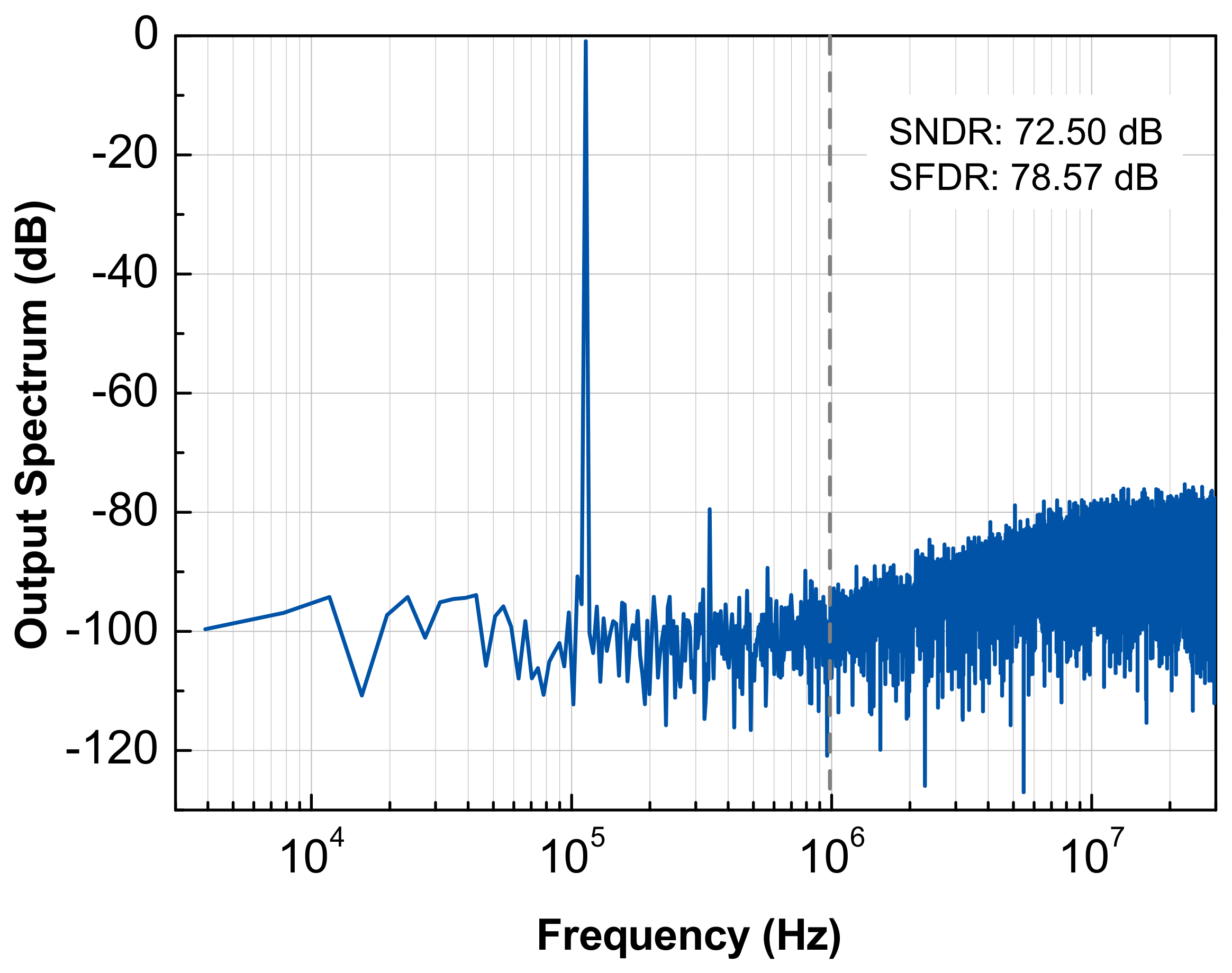
The simulated output spectrum of the proposed converter, fully implemented in a 28 nm CMOS technology, is shown in
Figure 17. With an oversampling ratio (OSR) of 32 and a 10-bit DAC, a peak of 72.5 dB in the signal-to-noise and distortion ratio (SNDR) was achieved for a ≈113 kHz input signal and a 1 MHz BW.
Table 3 summarizes the simulation results. The converter dissipated ≈112 μW, which could be translated into a Walden figure of merit,
, of 16.2 fJ/conv.-step.
These results are promising, allowing for a fully synthesizable ADC that is capable of achieving both high resolutions and good energy efficiency.
5. Conclusions
The most-suited high-resolution ADC topologies for IoT applications were described and compared in terms of complexity, overall performance, and energy efficiency. ΔM was described because it is the basis of some well-known topologies and has inspired others, such as SAR-ADC with NS or M ADC. Taking into consideration the advantages of standard-cell-based synthesizable schemes, some schematics of comparators and amplifiers were reported, and their key performance parameters were compared. An innovative topology, a digital-ΔM ADC employing NS, was detailed employing passive and standard-cell-based circuitry. An SNDR of 72.5 dB was achieved for a 1 MHz BW (OSR of 32) with an estimated of 16.2 fJ/conv.-step. Thus, a fully synthesizable ADC that is compatible with IoT applications was clearly demonstrated.
Author Contributions
Conceptualization: A.C., V.G.T. and J.G.; methodology: A.C., V.G.T. and J.G.; investigation: A.C., V.G.T. and J.G.; writing—original draft preparation: A.C.; writing—review and editing: all authors; supervision: V.G.T., P.B. and J.G. All authors have read and agreed to the published version of the manuscript.
Funding
This work was funded by National Funds through FCT—Fundação para a Ciência e a Tecnologia, I.P., through a Ph.D. Grant (SFRH/BD/137519/2018) and the following project references: UIDB/50025/2020-2023, SMART-E-PTDC/CTM-PAM/04012/2022, IDS-PAPER-PTDC/CTM-PAM/4241/2020 and PEST (CTS/UNINOVA)-UIDB/00066/2020. This work also received funding from the European Community’s H2020 program [Grant Agreement No. 716510 (ERC-2016-StG TREND) and 952169 (SYNERGY, H2020-WIDESPREAD-2020-5, CSA)].
Data Availability Statement
The data presented in this study are contained within the article.
Conflicts of Interest
The authors declare no conflict of interest.
References
- O’Riordan, N. Industrial IoT. In Circuits and Systems for the Internet of Things: CAS4IoT; IEEE CAS, River Publishers: Gistrup, Denmark, 2017. [Google Scholar]
- Jiang, D.; Sin, S.W.; Qi, L.; Wang, G.; Martins, R.P. Recent Advances in High-Resolution Hybrid Discrete-Time Noise-Shaping ADCs. IEEE Open J. Solid-State Circuits Soc. 2021, 1, 129–139. [Google Scholar] [CrossRef]
- Fredenburg, J.A.; Flynn, M.P. A 90-MS/s 11-MHz-bandwidth 62-dB SNDR noise-shaping SAR ADC. IEEE J. Solid-State Circuits 2012, 47, 2898–2904. [Google Scholar] [CrossRef]
- Schreier, R.; Temes, G.C. Understanding Delta-Sigma Data Converters; IEEE Press: Piscataway, NJ, USA, 2005; Volume 74. [Google Scholar]
- Ren, J.; Sarwana, S.; Sahu, A.; Talalaevskii, A.; Inamdar, A. Low-pass delta-delta-sigma ADC. IEEE Trans. Appl. Supercond. 2014, 25, 1–6. [Google Scholar] [CrossRef]
- Xu, Z.; Ojima, N.; Li, S.; Iizuka, T. An all-standard-cell-based synthesizable SAR ADC with nonlinearity-compensated RDAC. IEEE Trans. Very Large Scale Integr. Syst. 2021, 29, 2153–2162. [Google Scholar] [CrossRef]
- Park, J.E.; Hwang, Y.H.; Jeong, D.K. A 0.5-V fully synthesizable SAR ADC for on-chip distributed waveform monitors. IEEE Access 2019, 7, 63686–63697. [Google Scholar] [CrossRef]
- Aiello, O.; Crovetti, P.; Alioto, M. Fully synthesizable low-area analogue-to-digital converters with minimal design effort based on the dyadic digital pulse modulation. IEEE Access 2020, 8, 70890–70899. [Google Scholar] [CrossRef]
- Deloraine, E.M.; Van Mierlo, S.; Derjavitch, B. Methode et Systéme de Transmission par Impulsions. French Patent 932,140, 10 August 1946. [Google Scholar]
- Abate, J.E. Linear and Adaptive Delta Modulation. Ph.D. Thesis, Newark College of Enginering, Newark, NJ, USA, 1967. [Google Scholar]
- Zrilic, D.G. Circuits and Systems Based on Delta Modulation: Linear, Nonlinear and Mixed Mode Processing; Springer Science & Business Media: Heidelberg, Germany; New York, NY, USA, 2005. [Google Scholar]
- Carusone, T.; Johns, D.; Martin, K. Analog Integrated Circuit Design, 2nd ed.; Wiley: Hoboken, NJ, USA, 2011. [Google Scholar]
- Razavi, B. Principles of Data Conversion System Design; IEEE Press: New York, NY, USA, 1995. [Google Scholar]
- Rabuske, T.; Fernandes, J. Charge-Sharing SAR ADCs for Low-Voltage Low-Power Applications; Springer: Berlin/Heidelberg, Germany, 2017. [Google Scholar]
- Guo, W.; Sun, N. A 12b-ENOB 61 μW noise-shaping SAR ADC with a passive integrator. In Proceedings of the ESSCIRC Conference 2016: 42nd European Solid-State Circuits Conference, Lausanne, Switzerland, 12–15 September 2016; pp. 405–408. [Google Scholar]
- Li, S.; Qiao, B.; Gandara, M.; Sun, N. A 13-ENOB 2nd-order noise-shaping SAR ADC realizing optimized NTF zeros using an error-feedback structure. In Proceedings of the 2018 IEEE International Solid-State Circuits Conference-(ISSCC), San Francisco, CA, USA, 11–15 February 2018; pp. 234–236. [Google Scholar]
- Liu, J.; Wang, X.; Gao, Z.; Zhan, M.; Tang, X.; Hsu, C.K.; Sun, N. A 90-dB-SNDR calibration-free fully passive noise-shaping SAR ADC with 4× passive gain and second-order DAC mismatch error shaping. IEEE J. Solid-State Circuits 2021, 56, 3412–3423. [Google Scholar] [CrossRef]
- Correia, A.; Barquinha, P.; Marques, J.; Goes, J. A High-resolution Δ-Modulator ADC with Oversampling and Noise-shaping for IoT. In Proceedings of the 2018 14th Conference on Ph. D. Research in Microelectronics and Electronics (PRIME), Prague, Czech Republic, 2–5 July 2018; pp. 33–36. [Google Scholar]
- Weaver, S.; Hershberg, B.; Moon, U.K. Digitally synthesized stochastic flash ADC using only standard digital cells. IEEE Trans. Circuits Syst. I Regul. Pap. 2013, 61, 84–91. [Google Scholar] [CrossRef]
- Aiello, O.; Crovetti, P.; Alioto, M. Fully synthesizable, rail-to-rail dynamic voltage comparator for operation down to 0.3 V. In Proceedings of the 2018 IEEE International Symposium on Circuits and Systems (ISCAS), Florence, Italy, 27–30 May 2018; pp. 1–5. [Google Scholar]
- Ojima, N.; Xu, Z.; Iizuka, T. A 0.0053-mm2 6-bit fully-standard-cell-based synthesizable SAR ADC in 65 nm CMOS. In Proceedings of the 2019 17th IEEE International New Circuits and Systems Conference (NEWCAS), Munich, Germany, 23–26 June 2019; pp. 1–4. [Google Scholar]
- Aiello, O.; Crovetti, P.; Toledo, P.; Alioto, M. Rail-to-rail dynamic voltage comparator scalable down to pW-range power and 0.15-V supply. IEEE Trans. Circuits Syst. II Express Briefs 2021, 68, 2675–2679. [Google Scholar] [CrossRef]
- Li, X.; Zhou, T.; Ji, Y.; Li, Y. A 0.35 V-to-1.0 V synthesizable rail-to-rail dynamic voltage comparator based OAI&AOI logic. Analog. Integr. Circuits Signal Process. 2020, 104, 351–357. [Google Scholar]
- Christen, T. A 15-bit 140-μW Scalable-Bandwidth Inverter-Based ΔΣ Modulator for a MEMS Microphone With Digital Output. IEEE J. Solid-State Circuits 2013, 48, 1605–1614. [Google Scholar] [CrossRef]
- Ki, W.H.; Temes, G.C. Offset-compensated switched-capacitor integrators. In Proceedings of the IEEE International Symposium on Circuits and Systems, New Orleans, LA, USA, 1–3 May 1990; pp. 2829–2832. [Google Scholar]
- Nagaraj, K.; Vlach, J.; Viswanathan, T.; Singhal, K. Switched-capacitor integrator with reduced sensitivity to amplifier gain. Electron. Lett. 1986, 21, 1103–1105. [Google Scholar] [CrossRef]
- Chae, Y.; Han, G. Low voltage, low power, inverter-based switched-capacitor delta-sigma modulator. IEEE J. Solid-State Circuits 2009, 44, 458–472. [Google Scholar] [CrossRef]
- Correia, A.; Tavares, V.G.; Barquinha, P.; Goes, J. Trade-offs and Limitations in Energy-Efficient Inverter-based CMOS Amplifiers. In Proceedings of the XXXVI Conference on Design of Circuits and Integrated Systems (DCIS), Vila do Conde, Portugal, 24–26 November 2021. [Google Scholar]
- Neofytou, M.; Zhou, M.; Bolatkale, M.; Liu, Q.; Zhang, C.; Radulov, G.; Baltus, P.; Breems, L. A 1.9 mW 250 MHz Bandwidth Continuous-Time ΣΔ Modulator for Ultra-Wideband Applications. In Proceedings of the 2018 IEEE International Symposium on Circuits and Systems (ISCAS), Florence, Italy, 27–30 May 2018; pp. 1–5. [Google Scholar]
| Publisher’s Note: MDPI stays neutral with regard to jurisdictional claims in published maps and institutional affiliations. |
© 2022 by the authors. Licensee MDPI, Basel, Switzerland. This article is an open access article distributed under the terms and conditions of the Creative Commons Attribution (CC BY) license (https://creativecommons.org/licenses/by/4.0/).
