1. Introduction
Electronic engineering plays a crucial role in modern civilization in both the analogue and digital domains. This was made possible by the contribution of the circuit elements that are commonly called electronic components.
Figure 1 shows some examples of electronic components. Depending on their interactions with the other parts of the circuit, electronic components are often placed into two categories, namely, active and passive circuit elements. Active circuit elements are capable of generating electrical energy or power gain to the other parts of the circuit which include for example, transistors, operational amplifiers, integrated circuits, voltage and current sources, etc. Passive circuit elements can only use or dissipate the available power sources, for example resistor, capacitor, inductor, thermistor, light-dependent resistor (LDR), etc. In general, active circuit elements are capable of generating electrical power while passive circuit elements can only store, use or deny the generated power. Additionally, a transistor is an active device owing to its ability to generate power gain. These circuit elements altogether form electronic components (see
Figure 1) that have been a major bedrock for modern civilization owing to their tremendous contribution in the advancement of electronic industries. The three branches in
Figure 1, illustrate the generalized evolution of the electronic components accordingly. The first, second and third branches give, respectively, the fundamental circuit elements, semiconductor devices and many other components designed to achieve various circuit functionalities.
The transistor has been the leading component in electronic gadgets due to its reliable capabilities in switching, amplification and micro-scalability. The performances of an electronic device are improved by incorporating smaller and faster circuit components. This approach serves many purposes, for example portability and improved power consumption because fewer components are involved. However, transistor scaling is challenging as they are presently few nano-meters in size, hence the need for an alternative to transistors for future electronic systems design. Scalability of electronic components becomes an important factor in order to meet the increasing demand of reliable digital electronic systems. Currently, nano-scalability is one of the main challenges in the nanoelectronics industries [
1], especially due to the high demand of faster and more reliable systems (small, medium and large scales). For seven decades, transistors have been the leading component contributing to the exponential advancement in electronic systems and designs [
2]. However, modern transistors suffer from nano-scalability issues owing to their infinitesimal dimensions [
3]. The performance of devices and systems improves with the reduction in the size of their constitutive circuitries [
4] and often brings forth advantages such as reliability, lower power consumption, speed, cheapness, portability, etc., thanks to memristor nano-scalability.
The memristor is a two-terminal nonlinear dynamic electronic device and is typically a passive nano-device whose conductivity is controlled by the time-integral of the applied voltage (also known as flux) across it or the time-integral of the current (also known as charge) flowing through it. This new component was first envisioned by circuit theorist Leon Chua in 1971 and it is proclaimed to be the fourth basic passive circuit element (alongside the resistor, capacitor and inductor) having interesting features that make it suitable for various applications. For example: high-density memory applications, bio-electronics or bio-inspired applications, storage and processing of big data, and image recognition and processing. It is impossible to completely discard the transistor due to the emergence of the memristor because it is an active device while the memristor is a passive one. However, using both of them in a circuit will tremendously improve its performance, because one memristor can replace multiple transistors.
Memristive behaviour has been observed experimentally for two centuries but remained unidentified because no one had ever thought of the contingency of the fourth basic circuit element in electronics. The first human-made memristor dated in 1801 by English chemist Humphry Davy [
5], in which the fingerprint of a memristor manifested experimentally with a carbon arc discharge lamp (incandescent light) and was considered as the first artificial electric light source. Some devices and systems were shown to possess the now well-known signature of a memristive device (pinched hysteresis loop) owing to their inholding inertia [
6] which occurs from the movement of mobile ions or oxygen vacancies, the formation and splitting of conductive filaments and phase-change transition of some materials for data storage, e.g., sputtered
films [
7,
8]. This inertia causes latency in the system mechanism, resulting in the exhibition of its memory effects. Contemporarily, the memory effect is also seen in nano devices [
9] in which the dynamics of electrons and ions depend on the previous history of the device.
Leon Chua [
10] observed from symmetrical argument of the circuit elements (shown in
Figure 2) that for the sake of completeness there should be a fourth passive circuit element in addition to the conventional resistor, capacitor and inductor. He theorized the existence of the memristor and its electromagnetic interpretation. However, the memristor differs from the three other passive circuit elements in the sense that it is a nonlinear element and capable of storing information. As clearly presented in [
10], some theories were established supporting the existence of the fourth basic circuit element, its electromagnetic interpretation and some promising applications. Few years later, Chua and Kang [
11] elaborated a broader class of nonlinear systems called the memristive systems, as discussed in
Section 3.
Although the principle theories of memristor exist [
10], its realization remained a mystery for nearly four decades. Then in 2008 [
12], a team of researchers from the Hewlett Packard (HP) laboratory led by Stanley Williams published a paper in
Nature Journal announcing their successful realization of a two-terminal solid-state device bearing the characteristics of the memristor described by L. Chua in 1971 [
10]. This discovery, which is described as accidental while working on nano crossbar grid [
3], paved the way for more awareness that continued to attract the global attention of many researchers, engineers and scientists, therefore exploring more possible features of the memristor in terms of applications and technologies. Some memristor technologies include the Redox reaction, Ferro-electricity, Organic chemistry, etc., and will be discussed in
Section 4. The conventional resistance to the flow of charges through a conducting material or wire is often analogously described to flowing water through a pipe of uniform cross-sectional area. The analogy of memristance with respect to the flowing charge is seen in flowing water through a pipe having a variable diameter [
13,
14]. The volume of water flowing through the pipe increases with increasing of the pipe’s diameter, hence the water encounters a lower resistance path, while it decreases with decreasing of the pipe’s diameter, hence encountering a higher resistance path.
The memristor is seen as the most promising element, not only capable of replacing transistors for some applications, but also to revolutionize electronic industries virtually in every facet of electronic systems, design and applications [
3]. Hence, memristor becomes a suitable component for nanotechnology. The most common properties that make memristor a good candidate for future technologies are: Nano-scalability, Memory capabilities, Conductance modulation and Nonlinearities whose contemporary demand is at its peak. For example, transistors suffer nano-scalability limitations due to their finite dimensions while it would be required that they can be of infinitesimal dimensions. Therefore, they cannot effectively undergo any further reduction in size as they are presently a few nano-meters [
15]. As stated by Gordon Moore, co-founder of Intel corporation, “The number of transistors incorporated in a chip should approximately double every 24 months”and hence is called Moore’s Law. This law holds only if the sizes of chips associated with circuitries keep reducing, otherwise the law will cease to be true. Transistors are tiny electrical switches, forming the fundamental unit that drives all electronic gadgets. As the transistors become smaller, they also become faster and require less electricity to operate. Clearly, there will be a limit when transistors cannot undergo any further reduction in size, which seems to be different with memristor nano-scalability.
However, the memristor discovery in [
12] is still under criticism as some researchers are not convinced about the memristor [
16,
17]. The researchers in [
18], tried to prove that the real memristor stated in [
10] is not identifiable and even an impossibility. Intuitively, the three known basic passive circuit elements (resistor
R, inductor
L and capacitor
C) are unquestionably independent of one another and they are in existence naturally, hence referred to as the fundamental circuit elements. However, on the other hand, the claim for memristor as the fourth fundamental circuit element is challenging owing to its one-to-one resistor dependencies [
19]. Namely, it bears the exact same unit of measurement as the ohm
and a deductive-like expression, as:
it very much resembles a resistor, hence memristor is the portmanteau of memory resistor. Here
is the memristance and it is expressed in ohms (
) as is a resistor.
Notwithstanding, the fact that a memristor cannot be realized by any simple combination of the three basic circuit elements (
R,
L and
C) proves that the memristor is actually a fundamental circuit element [
3]. Although its position as the fourth fundamental passive circuit element is challenging [
18,
19], the memristor bears a massive technological impact and it appears to be a good candidate for numerous designs and applications. Moreover, since its inception in 2008, thousands of publications were published on memristor technologies and applications (too many to be cited) and in doing so, they affirmed memristor as the fourth basic circuit element. The number of memristor publications grows exponentially, hence outweighing the few criticisms.
This study is organized as follows.
Section 2 presents briefly the three known basic passive circuit elements and is then followed by the memristor argumentation as the fourth basic passive circuit element and its description by mode of excitation.
Section 3 presents memristor insights and its strong philosophical criticism, especially when it is referred to as the fourth basic passive circuit element.
Section 4 introduces the memristor technologies and a thorough description and analysis of TiO
memristor.
Section 5 presents analog and SPICE models of the memristor useful for demonstrations and simulation of memristor-based applications.
Section 6 presents the modeling of memristor as a function of the flowing charge through it.
Section 7 presents some interesting application areas of the memristor. Finally, the results and the contents of this paper are discussed in
Section 8.
2. The Basic Passive Circuit Elements and Memristor Argumentation
This section presents briefly the three familiar fundamental passive circuit elements, namely resistor
R, inductor
L and capacitor
C and is then followed by the memristor argumentation as the fourth fundamental passive circuit element. The voltage
V and current
i sources are the basic active circuit elements in the form of dependent or independent sources. We first recognize the relationship between electric voltage
V and magnetic flux
, as typically known from Faraday’s law, as:
that is,
where
, is the initial flux at time
and may be zero or nonzero. Similarly, the relationship between electric current
i and electric charge
q is conventionally known as;
⇒
where
is the initial charge at time
and may be zero or nonzero. Hence, these four variables, namely voltage
V, current
i, magnetic flux
and electric charge
q are called the fundamental circuit variables. Each pair of these four circuit variables are interrelated by the basic passive circuit elements via a constitutive relationship of the form
characterizing the port equations of their circuit functionality, where
n and
m are any of
V,
i,
or
q circuit variables.
Figure 2 illustrates the symmetry argument of the four basic circuit elements with respect to the four circuit variables. In the case of resistor
R, it can be seen that
m and
n are voltage and current, respectively, and is given by the constitutive relationship
. Similarly, the constitutive relationships of capacitor
C and inductor
L are
and
, respectively. However, there is a possible missing relationship between magnetic flux
and electric charge
q.
In 1971, Leon Chua proposed that for the sake of completeness there must be a fourth fundamental passive circuit element which gives the missing relationship between
and
q, thus having a constitutive relationship:
or equivalently as
, where
M is the Memristor, a portmanteau of ‘memory’and ‘resistor’. The naming of the fourth basic passive circuit element as memristor (memory resistor) portrays that it has the property of resistance with memory. This fact arises due to the peculiar nature of memristor to remember the history (memory effect) of its previous state (resistance), even after the power is disconnected and restarted from this previous state after the power is reconnected, irrespective of the duration upon which the power is ON or OFF (i.e., it could be a day, a month or years) [
3]. This special property suggests the memristor as a promising element in memory applications.
These four circuit variables in conjunction with the four passive circuit elements produced a set of six possible equations, one equation more than the previous five already known equations, due to the presence of memristor. We know details about resistors, capacitors and inductors. Therefore, in the following, these familiar passive circuit elements are introduced briefly, while the memristor is evaluated comprehensively.
2.1. Resistor
The resistor is a passive two-terminal basic electronic component discovered by Georg Simon Ohm in 1827, in which, at a constant temperature, the current flowing through these terminals is directly proportional to the voltage drop across it. Resistance is an inherent property of a material that resists the flow of electric charge (or electric current) through it, dissipating power in the process as heat. It is measured in Ohm (
) named after the inventor. Resistors are components designed basically to offer resistance in the circuit, commonly used as a current-limiting device. Virtually every electronic circuit is composed of at least one or more resistors, either a real component or by choosing the type of the material itself (resistivity). Currently, there are many types of resistors suitable for different applications, for example:
Fixed resistor, Rheostat or Variable resistor, Potentiometer (pre-set or post-set), Thermistor, Varistor, Thermocouple, Photo resistor or Light-Dependent Resistor (LDR), Voltage-Dependent Resistor (VDR), Barretter, Strain gauge, etc. Some of them are nonlinear such as: Thermistor, Varistor, Photo resistor, etc. Resistors are characterized by: the resistance, the tolerance, the maximum working voltage, the power rating, the temperature coefficient, the noise, and even an inductance effect [
20].
2.2. Capacitor
The capacitor is the first passive two-terminal basic electronic component invented by Ewald Georg von Kleist in 1745. It comprises two conductive materials separated by a dielectric. The dielectric could be air or any appropriate insulation material. Condenser is almost synonymous to capacitor, condenser being for the circuit element, capacitance for the electric characteristic, and these terminologies are often used interchangeably. Capacitance characterizes the amount of charge stored in the condensator between two parallel conducting materials subject to potential difference, and is measured in Farad (F) often used with sub-multiple prefixes such as micro (), nano (n), pico (p), etc. As with resistors, there are many different types of capacitors used for different applications. For example: Ceramic capacitor, electrolytic, film, Tantalum, Silva Mica, variable, SMD capacitors, etc. Capacitors have been used extensively in areas such as: power conditioning, signal processing, energy storage, coupling, filters, tuning radios and resonance, sensors, output regulation of power supply, etc.
2.3. Inductor
The inductor is a passive two-terminal basic electronic component discovered by Michael Faraday in 1831. It is capable of storing energy in the form of a magnetic field due to the passage of an electric current through it. Any current-carrying conductor is associated with a magnetic field circulating around the conductor. The strength of the field or magnetic flux is directly proportional to the magnitude of the electric current flowing through it. A straight coil wire has one turn and as such, it has less inductance. Moreover, the generated magnetic field becomes more significant if the wire is coiled to a certain number of turns. However, the field is more concentrated if the coil is wound on a ferromagnetic material (or iron core format) and has a higher inductance. Additionally, due to the variation of the formed magnetic flux, a voltage (self-induced voltage source according to Faraday’s law) is induced in the coil and acts in such a way to oppose itself to any change in the current that causes it (according to Lenz’s law). Similarly, there are various types of inductors made in different sizes and shapes, and some are sorted by the kind of applications and the type of winding and core materials. Power inductors are larger than general purpose inductors. In addition to storage of energy, the inductor is used extensively in numerous applications, such as: transformers, induction motors, relays, radio tuning, television, filters, transmission systems, sensors and many other applications in conjunction with capacitors and resistors.
2.4. Memristor
Memristor is claimed to be the fourth basic circuit element [
10] (alongside the resistor, capacitor and inductor). It is a nonlinear passive two-terminal electronic component defined by the relationship between the magnetic flux linkage
and the electric charge
q. The definition of a
memristor is given by its pioneer [
21], as: “
any 2-terminals device, exhibiting a pinched hysteresis loop which always passes through the origin in the voltage-current plane when driven by any periodic input current source, or voltage source, with zero DC component. If the input is a current source, it is called a current-controlled memristor. If it is a voltage source, it is called a voltage-controlled memristor ”. The name memristor is the contraction of memory resistor owing to its peculiar nature to resist the flow of electric current (as achieved by a resistor) and at the same time to remember the last amount of charge passed through it at the time when the power was disconnected, hence to memorizing the previous device resistance. Memristor keeps track of its dynamic resistance with respect to the current or electric charge flowing through it.
From the memristor symbol, see
Figure 3, the unmarked side (the plus sign terminal) and the marked side (the minus sign terminal) indicate, respectively, the higher and lower potential terminal [
22]. Memristor is a non-symmetrical two-port element, the polarity reversal and its effect from the application perspective was demonstrated [
23]. This is very important for someone to consider before using a memristor in certain applications, e.g., biomimetic system [
24].
Recall that the magnetic flux
represents the time-integral of voltage
and the electric charge
q is the time-integral of electric current
, hence these quantities are to be determined between two reference points. The fact that memristor is always defined by the integral of its input and output quantities (
and or
), explains in essence why memristor remembers its previous resistance or has a memory effect. The constitutive relationship of a memristor is expressed as
, where
M is the memristance that is short-form for memory resistance. Memristance is the property of a memristor to remember its previous resistance state. It is defined by the functional relationship between magnetic flux
and electric charge
q, and is measured in Ohms (
), the same measurement unit as resistance. The instantaneous memristance can be deduced from the dynamic slope of the
-
q locus given in the
-
q plane as shown in
Figure 4. The relationship between the magnetic flux
and the electric charge
q could be expressed in two forms depending on the modes of excitation, namely:
for a charge-controlled memristor (i.e., memristor device excited by a current source) or
for a flux-controlled memristor (i.e., memristor device excited by a voltage source), where
and
are nonlinear functions denoting memristance and memductance, respectively.
The resistance of the memristor (or memristance) changes dynamically with the amount and direction of current flowing through it. People often confuse memristance with resistance. However, memristor differs from resistor in the sense that:
It has entirely different constitutive relationship in comparison to resistor.
Its resistance changes according to the quantity of charges having previously passed through it.
Its resistance changes according to the direction of electric current flowing through it because it is not a bilateral device. Therefore, its connection mode matters.
It preserves the previous history of electricity, according to the charge passed through it previously, at any given time. In other words, it has memory of the previous electricity passed through it (memory effect).
It is nonlinear in nature.
It has pinched hysteresis loop in the voltage–current response in a circuit, depending on its initial condition. Moreover, memristor has different circuit response according to its initial condition.
It cannot be realized by any combination of the three known circuit elements (capacitor, resistor and inductor) and hence it can be considered as “fundamental”.
It has a unique nature for the relationship between magnetic flux and electric charge (which is not directly available by measurement).
It behaves differently in DC and AC conditions.
Nevertheless, the memristor and resistor share some similarities, for example:
Both offer resistance to the flow of electric current.
Their quantities (i.e., memristance and resistance) have the same unit of measurement, i.e., Ohms, symbol: .
No phase shift in their voltage and current wave-forms, because ⇒ and vice versa.
They both dissipate energy as heat (Joule effect). They are not loss-less devices, i.e., without preservation of energy. They are always associated with power (P) intake, i.e., .
3. The Memristor Insights and Its Philosophical Arguments
A broader class of nonlinear systems is reported [
11], called memristive systems in which some nonlinear dynamic systems were found to exhibit memristive behavior. Additionally, systems whose resistance depends on its internal state (e.g., temperature) are believed to be memristive. Examples of these systems are:
Thermistor,
Discharge tube,
Hodgkin–Huxley (or Ionic) System and
Tungsten filament lamps. The memristive systems are generally described by one-port and state equations:
where
u is the input to the system,
y is the output of the system,
x is a vector denoting the set of internal state variables of the system,
f is a nonlinear vector function and
g is a nonlinear scalar function. Equation (
4) affirms that memristive systems are nonlinear systems because the function
f depends nonlinearly on the dynamic state variable
x and both functions (
f,
g) depend on the input
u to the system. Notice that Equation (
4) describes a time-variant system, so all the variables are also functions of time. For time-invariant memristive systems, Equation (
4) is rewritten as follows:
Moreover, an ideal memristor is considered as a special case of a memristive system which can be expressed as:
where the state variable
x depends solely on the time-integral of the voltage applied across the device or the time-integral of the current flowing through it, for a flux-controlled and charge-controlled memristor, respectively.
In
Figure 5, a two-terminal device under test (
) is subjected to a periodic input source
, where
could be voltage or current source as highlighted in the aforementioned definition of memristor. If the current–voltage response of
Figure 5 on the left corresponds to that of
Figure 5 on the right, for any
source respecting the definition in [
21], then the black box is called a
memristor. More details to check whether a candidate system is indeed a memristive system are given in the following.
3.1. Fingerprints of a Memristor
Circuit elements such as the resistor, capacitor, inductor, etc., are often characterized by their voltage–current response (
V-
I characteristics) in any given circuit. Memristor is not an exception, it has a peculiar voltage–current response which is a unique identifier that distinguishes it from any other known circuit element. Hence, it is called the fingerprint of a memristor and is used to characterize a memristive system. The most three well-known memristor fingerprints are enumerated in [
25,
26,
27], as:
The V-I response of a memristor (with positive memristance) is always a pinched hysteresis loop (Lissajous figure) when subjected to a bipolar periodic input signal without offset.
The hysteresis lobe area decreases monotonically when the excitation frequency increases.
For a fixed-input amplitude, the pinched hysteresis loop shrinks to a single-valued function as the frequency of the input supply tends to infinity.
Figure 6 illustrates the mentioned three figerprints of a memristor. More fingerprints of an ideal memristor are given in [
26], including constitutive relationship (CR) between flux and charge and parameter versus state map (PSM) [
28]. In fact, nine fingerprints of memristor are given in [
26] including the three above mentioned and they give birth to a valid test for assessing a memristor device. In the following, we give the description of a pinched hysteresis loop and pinched hysteresis lobe area.
3.1.1. Pinched Hysteresis Loop (PHL)
The voltage–current response of a memristor in a circuit is always a pinched hysteresis loop [
27,
29]. As seen in
Figure 6a, the maxima and minima of the current
and voltage
, through and across the memristor, respectively, are not reached simultaneously and this is the cause of the formation of the hysteresis lobe area. The term
pinched hysteresis loop (or PHL) refers to a double-valued Lissajous figure in the voltage–current (V–I) plane which is always pinched at the origin for any given time, for any initial condition, for any input amplitude (voltage or current) and for any input frequency [
28]. The term
pinched also signifies that
whenever
and vice versa. In other words, for any given value of current
, there will be two corresponding values of voltage
except at
. The converse is also true, for any given value of voltage
, there will be two corresponding values of current
except at
. This can be observed from
Figure 6a: it shows that current (
in orange) is zero whenever the voltage (
in black) is zero and as a result the hysteresis loop always passes through the origin, see
Figure 6b.
It turns out that memristive systems exhibit two different kinds of PHL [
25,
26] depending upon the system’s constituents (i.e.,
f and
g as defined in Equation (
4) and the type of excitation (odd-type or even-type) [
26]. The two types of PHL are Self-crossing PHL (also known as Transversal or crossing PHL) and Tangential PHL (also known as non-tranversal or non-crossing PHL).
- i.
Self-crossing or transversal pinched hysteresis loop (SPHL): In this type of PHL, the locus cuts across at the origin (or pinched point). Additionally, one can see that the slope of the locus moving toward the origin is different from that of the locus leaving the origin.
Figure 7a shows a typical transversal PHL. An example of memristive system with transversal pinched hysteresis loop is the mathematical model of HP memristor (presented in
Section 4).
- ii.
Tangential or non-transversal pinched hysteresis loop (TPHL): As the name implies, the locus does not cut across, rather it passes tangentially as confirmed by the arrow directions, see
Figure 7b. Notice that it is still pinched at the origin, i.e.,
whenever
and vice versa, however, there is always a fixed slope (for both the two slopes, i.e.,
and
) when the locus moves toward the origin and immediately after leaving the origin. This observation is clear because the separate line slopes coincide together before reaching the origin and remain together even after leaving the origin until a certain amount of voltage or current is reached, then the loci separate and hence the hysteresis lobe area becomes visible, see
Figure 7b.
There are many memristive systems whose current–voltage response is a tangential PHL, some of these systems being mentioned in [
11,
25,
30]. Moreover, tangential PHL is met in the memristive behavior of plants (Aloe vera and Mimosa pudica) [
31]. However, it is reported that the pinched hysteresis loop of an ideal memristor, memcapacitor and meminductor is always a self-crossing PHL [
32]. It is even emphasized that self-crossing PHL is another signature or fingerprint of an ideal memristor. Moreover, TiO
memristor (from HP lab [
12]) and SDC memristor (from KNOWM [
33]) are examples of a memristor with a self-crossing PHL.
3.1.2. Pinched Hysteresis Lobe Area
The hysteresis lobe area decreases when the input frequency increases. Recall that the memristor is a nano device, therefore, a small input signal is enough to generate a large electric field to trigger the device according to:
, when
x is the internal state and corresponds to the displacement of charge carriers. Therefore, any small increment in the potential difference
V leads to a large magnitude of electric field
to be generated. However, the resistance of the memristor depends on its internal state, hence any change in the input signal results in a behavioral change of its internal state as well. Therefore, for example considering an input current
such that:
the flowing charge is:
where
is the initial charge just before the current starts to flow and
is the charge delivered by the current source during the first quarter of the period
and the magnitude peak-to-peak of the flowed charge is given by:
For an ideal charged-controlled memristor, its state variable is rather the charge flowing through the device. It is obvious from Equation (
9) that increasing the frequency
for a fixed amplitude
, leads
peak-to-peak amplitude to decrease significantly and hence causes the shrinkage of the pinched hysteresis loop towards a linear graph.
Figure 8a shows the effect of increasing input frequency on the PHL lobe area of the memristor. The input frequency
is considered in three steps
,
and
with the corresponding lobe areas
,
and
, respectively, such that:
and
It follows that: as
,
, this behavior is shown in
Figure 8b.
The pinched hysteresis lobe area can be calculated. Let us consider a memristor excited by a current source given by
with
,
T being the period. By considering a half cycle (i.e.,
) of the input
, the hysteresis loop is given in
Figure 9, having an enclosed area
A and surface boundary
S, altogether enclosed in a triangle
[
34,
35,
36].
The area
A is obtained from the surface integral of the voltage with respect to the current, as:
Figure 10 shows the operating point of a memristor in the plane (
q,
) starting with an initial charge
, corresponding to an initial flux
, with the so-called shifted flux
. Let us use a shifted charge
, then:
From Equations (
9) and (
11), the operating point is within the interval
, hence the normalized form of the constitutive relationship becomes:
The corresponding normalized expression of the memristance-versus-state map, becomes:
From Equations (
7) and (
8), the algebraic relation between the charge
and the current source
is:
From Equation (
10), with
, the area during the first half-cycle can be expressed as:
The integration by parts gives:
where the dot in
represents the derivative with respect to time. In [
34], the authors consider that the memristance function
can exhibit step discontinuity points
in the charge interval [
], with
, hence, they considered some step changes of the memristance at point
. However, the following excludes the case of any discontinuities for
. In this simplified case, the first term of Equation (
14) is zero. Noting that
, Equation (
14) gives then:
For example, the pinched hysteresis lobe area of the memristance expression is given in [
34] and is described in the following. The given memristance function is rewritten as:
where
,
is the initial memristance at time
and
is the charge necessary for the modification of the memristance by the value
[
34]. Since
is constant, then
. Using the current source (
7), then:
Using the identity:
, then
and the area is finally expressed as:
The area is independent of the initial memristance, however, it is directly proportional to the cubic power of the exciting current and inversely proportional to the input frequency. Note that Equation (
17) is determined according to the mathematical model of HP memristor, thus
is the charge required to move the tunneling dopant barrier between the doped and undoped region from
toward
(see
Section 4 for more details).
Moreover, a generalized formulation for computating the hysteresis lobe area of
mem-elements is reported in [
35], taking into account whether the input is a voltage or current. Thus, for a mem-element having input
, output
, state variable
and a differentiable function
, this mem-element can be characterized by:
where:
Thus, the loop area during the first half-cycle is given by:
3.2. Memristor by Mode of Excitation
Depending on the type of excitation, memristor can be characterized as charge-controlled memristor (CCM) or flux-controlled memristor (FCM), see
Figure 11.
3.2.1. Charge-Controlled Memristor (CCM)
For a charge-controlled memristor, the input applied to the memristor is a current source. The set-up is given in
Figure 11a, whereby a current source
is connected to a memristor
M. Thus, the current flowing through the memristor will cause a voltage drop
across it. From Equation (
4), the three variables
u,
x and
y become
i,
q and
v, respectively,
q being the time domain integral of the input current
i and
v the output voltage of the memristor. Hence, the constitutive relation of charge-controlled memristor should always represent the flux (
) dependence on the charge (
q), as:
Substituting the variables
i,
q and
V into Equation (
6), then:
Note that the notation
in Equation (
20) stands for a function definition: it could be any letter, for example
f, such that:
, so the (^) will often be removed in the following. Furthermore, notice that Equations (
20) and (
21) are identical, with
a charge-controlled memristance whose expression can be obtained by differentiating both sides of Equation (
20) with respect to
t:
. As the right hand side is a composite function, it can be seen that:
Therefore,
. This equation can be rewritten conveniently as:
Moreover, (
22) also gives the voltage drop
(see
Figure 11a) across the charge-controlled memristor
:
, such that:
Example 1. Suppose a charge-controlled memristor is characterized by the cubic function as follows:where the α and β are in and , respectively, ( and C mean Weber and Coulomb, respectively). Equation (25) is a modified version of the one used by Chua [28], by adding parametric coefficients α and β in order for the equation to be homogeneous. It implies that: Let the input current be: , then the charge is computed as follows: Knowing and , then and can be calculated from Equations (24) and (26), respectively. Hence, is the memristor initial charge that determines its previous state. Figure 12 shows some examples for , , , and two different values of as and , respectively, shown by Figure 12a,b. It is expected that taking different values for
, the operating point in
Figure 12(a1) will be changed, as will the hysteresis curve of
Figure 12(a3), compare
Figure 12a,b.
3.2.2. Flux-Controlled Memristor (FCM)
Memristor is flux-controlled if the input applied to the memristor is a voltage source (see
Figure 11b). The applied voltage
causes current
to flow through the memristor
M. One can see that the triad variables
u,
x and
y in (
6) become
V,
and
i, respectively. Hence, the output of a flux-controlled memristor is current and its constitutive relationship represents the charge dependence on flux. The constitutive relationship of the memristor of this type is given in (
28). The state variable is controlled by the flux as the result of time-domain integral of the applied input voltage.
Similarly, substituting the variables
V,
and
i into (
4), it gives:
where
is the flux-controlled memductance, measured in Siemens S, the same S.I unit as conductance. Note that
is the inverse of
. Thus,
is the time-domain integral of
V:
Similarly, the expression of
can be deduced by differentiating both sides of Equation (
28) with respect to time. Therefore,
, that is:
with
The current through the memristor
can be expressed from Equation (
30), and is finally given by:
Example 2. Suppose a flux-controlled memristor described by: and are appropriate constants in and , respectively. Given a source voltage: , the equivalent expression of the flux is obtained to be: . Using (31), then: Hence, knowing
, then
is calculated and some examples are given in
Figure 13a,b, respectively, for
and
. Similar to
Figure 12, here the initial conditions also affect the
-
q operating point and hence the
I–
V curve.
3.3. Memory Elements (Mem-Elements)
The emergence of the memristor led to the discovery of two other memory elements [
9], namely:
Memcapacitor and
Meminductor [
37,
38,
39]. The memristor
is not a loss-less device while the memcapacitor
and meminductor
are loss-less devices. Their names are derived accordingly from the conventional three circuit elements (resistor, capacitor and inductor, respectively) due to some common features, for example, each having the same unit of measurement as Ohm, Farad and Henry, respectively.
This poses the question of whether the memristor is indeed the fourth circuit element due to its resistance dependency and the appearance of memcapacitor and meminductor. Instead of four circuit elements, why not six altogether? However, the memristor, memcapacitor and meminductor are classified as memory circuit elements or simply mem-elements owing to the ability to remember their previous history, which is a manifestation of their memory effects [
40,
41,
42,
43,
44].
Due to the relation for capacitor and for inductor, the memory for these elements is already present by the occurrence of the time derivative (of voltage V for capacitor and of current i for inductor). This is not the case for through a resistor, and this is the heart of all interests for the new element: the memristor. Notwithstanding, circuit elements can be classified into linear and nonlinear elements. Hence, resistor, capacitor and inductor are rather linear elements, whereas memristor, memcapacitor and meminductor are nonlinear elements.
3.4. Not Every Nonlinear Dynamical System Is an Ideal Memristor
Memristive systems are a class of nonlinear dynamical systems whose current–voltage response resembles the fingerprint of an ideal memristor. However, it is known that not every nonlinear dynamical system is ideally a memristor, even though it exhibits a pinched hysteresis loop in its current–voltage characteristic. Hence, the above outlined criteria of memristor identification are not enough to distinguish a memristor device from some nonlinear dynamical systems that are not associated with a memristor. As recalled earlier, the pinched hysteresis loop is the major criterion used to authenticate a given system as memristor or not [
25]. In fact, it states that some memory elements may not exhibit pinched hysteresis loop, and an example of a memcapacitor is even given in [
45]. There are concerns in the scientific community regarding what a memristor is and is not [
16,
17,
18,
19], and further elaborations by Blaise Mouttet and Pershin et al. [
46,
47,
48,
49,
50] are explained in the following.
Leon Chua generalized the concept of memristor to include all resistance switching memories [
28]. However, it is shown experimentally that resistance switching memories are not memristors [
46]. Blaise Mouttet reported that L. Chua contradicted himself in [
28], against their axiomatic definition of a memristor in 1971 [
10]. He further concluded that the HP’s memristor lacks scientific merit [
17].
It is further clarified that the pinched hysteresis loop as the fingerprint of a memristor, or a memristive device, must hold for all amplitudes, for all frequencies, and for all initial conditions, of any periodic testing waveform, such as sinusoidal or triangular signals, which assume both positive and negative values over each period of the waveform [
29]. However, still some dynamical systems fulfilling these conditions are yet not memristor [
47,
48]. Notwithstanding, a simple testing technique to identify an ideal memristor is reported in [
50], which could, together with the concept of pinched hysteresis loop, help to identify a memristor from a non-memristor. However, there is no memristor reported in the literature, adhering to the axiomatic definition that relates charge and flux. Therefore, we may conclude that all the reported memristors are resistive switching devices and they are a special class of memristive systems, hence not an ideal memristor. The fact that an ideal memristor is not yet found and/or simply does not exist, does not discredit the hitherto findings regarding the memristor, as they are still valuable in resistive random access memory (ReRAM) and many other applications, and justify all efforts to better understand this new element.
An ideal memristor is described axiomatically by the constitutive relationship between the charge and the flux, but there is not yet a memristor discovery based on this principle. Contemporarily, all the memristor technologies are based on bipolar resistance-switching mechanisms. This is the main reason used by some scientists to criticize the memristor discovery. In fact, when one considers the existence of an ideal memristor, a possible conclusion is that such a device is likely to be impossible. Optimistically, we believe that one-day such a device will be discovered. However, for the moment, all the memristors are resistance-switching devices with potential applications. Moreover, because they possess the signatures of an ideal memristor, they can be categorized as a special class of memristive system.
4. Memristor Technologies and Models
All memristor technologies follow similar principles of operation—called
bipolar resistance switching, which means resistance switching between two limits, namely:
and
accomplished by the evolution of the applied signal.
is the lower resistance limit (higher conducting state) while
is the higher resistance limit (lower conducting state). Although the principle of operation is the same, each technology differs from one another in terms of resistance-switching mechanism (see
Figure 14).
The HP memristor also known as TiO
memristor uses the principle of a Metal-Insulator-Metal (MIM) device in which a bilayer of titanium oxide (TiO
) is placed between two platinum metal electrodes, as illustrated in
Figure 15b [
12]. One layer of the TiO
bilayer is doped with positive oxygen vacancies which allow for high conduction and the other layer is pure TiO
. Therefore, the formation exhibits two limiting resistance states (
and
) due to the contraction and the expansion of the doped region. Following the discovery of TiO
memristor [
12], many memristor technologies are reported using different switching mechanisms.
Figure 14 shows the taxonomy of memristor technologies. The memristor technologies are based on ionic or magnetic effects.
For example, the self-directed channel (SDC) device (the KNOWM memristor) uses electropositive metal (e.g., Silver, Ag) for conduction and the resistance-switching transition is due to the formation and dissolution of a high conducting channel filament [
13,
33]. This is the only memristor chip available yet for purchase, see
Figure 16. This is the chip used in the experimental demonstrations in
Appendix A.
Other memristor technologies include the following. The ferroelectric memristor is based on a ferroelectric tunnel junction where the tunneling conductance allows for bistable resistance-switching transition and can be tuned according to the duration and amplitude of the applied voltage [
51,
52,
53]. The memristive behavior was demonstrated experimentally and is attributed to the field-induced charge redistribution at the ferroelectric/electrode interface, which causes the modulation of the interface barrier height. Other memristors named according to fabricating materials, such as, the polymeric (or organic) [
54,
55], spintronic memristor [
56,
57], amorphous silicon memristor technology [
58] and amorphous oxide semiconductor zinc–tin-oxide (ZTO) memristor [
59]. In the following the TiO
memristor is considered due to its simpler modeling equations.
4.1. HP (TiO) Memristor: Modeling, Analysis and Interpretation
The TiO
memristor is the first discovered two-terminal solid-state memristor observed from a nano crossbar array of wires (see
Figure 15a) in which each junction formed a memristor [
3,
60]. It was demonstrated that the memristor in the crossbar can act as a storage element to give binary output for color images or as a switch to produce different grayscale levels, allowing the processing of images [
61].
Figure 15b shows the schematic of TiO
memristor [
12]. It is made up of a thin film bilayer of Titanium-Oxide TiO
of thickness
D sandwiched between two platinum (Pt) contacts which serve as electrodes. One portion of TiO
is initially doped with oxygen vacancies, and hence becomes TiO
and the other portion remains pure TiO
. These oxygen vacancies allow the layer to become an N-type semiconductor with electrons as charge carriers and thus adopt conductivity, the other undoped side has resistive properties, such that the entire arrangement behaves as a semiconductor material. Notice that in reality the dopants are scattered along the device width, however, its concentration in one edge is negligible compared to that of the other edge, creating two different resistive regions.
The structural arrangement constitutes two resistances
and
connected in series, as illustrated in
Figure 17.
resistance corresponds to the doped region (TiO
, i.e., higher conducting region) of width
while
resistance corresponds to the undoped region (TiO
, i.e., lower conducting region) whose width is
. Note that when
,
and if
,
. The boundary between doped and undoped regions (shown with two headed arrows) moves back and forth depending upon the direction of the flowing current or the polarity of the applied voltage. If the boundary moves leftward,
w decreases and the opposite width (
) increases, leading hence to higher resistance. Conversely, if the boundary moves rightward,
w increases while (
) decreases, leading hence to lower resistance. This further confirms the bipolar resistance-switching characteristics. Therefore,
w acts as the state variable of the device characterizing the instantaneous memristance.
Owing to oxygen vacancies, the electrons, with mass
and charge
, act as the charge carriers and are accelerated with an electric field:
and eventually stopped as they collide together. Their limiting speed
is given by
, where
is the mobility of the charge carriers and
is the average time between two consecutive collisions. The expressions of the voltages
and
across the doped and undoped regions can be expressed, respectively, as:
and
Note that the electric field in the conductive region can be expressed as
. The charge carriers expand then the doped region towards the right corresponding to an increase in the width
w with a positive current
such that:
where:
is the voltage across the two-port device,
is the current flowing through it,
is the memristance. Note that
and
is the drift speed of the boundary. The dopant mobility
determines how quickly the boundary between doped and undoped regions (or the dopants) can move back and forth across the device for any applied signal. The tunneling of the barrier width
w is determined by the magnitude and polarity of the applied voltage or current. It can be seen from Equation (38a) that at any given time
t, the width
of the doped region depends on the quantity of electric charge having passed through the device.
Finally, with the normalized form
, the modeling Equations (38) become:
where
.
if
and
if
. Equation (39c) shows that the HP memristor model remembers the coordinate of the state variable
x instead of the charge, however, the coordinate of
x is related to the quantity of charge having flowed through the device. Hence
x and
are directly proportional to one another. When a signal is applied to the device, the boundary between the doped and undoped regions moves, the direction of this movement depending on the polarity of the applied signal. Recall that the memristance is always positive, therefore it is always expected that:
or
. Integrating Equation (39a) for
x from 0 to 1, it can be seen that:
where
is the charge scaling factor which is required to move completely the doped/undoped boundary from
to
[
62]. Equation (39a) is rather rewritten as:
and this model is called the linear dopant drift model.
4.2. Window Function
There exists enriched intrinsic nonlinearity within the memristor device which also manifests in its hysteretic behavior [
12], however, when the dopants move toward either of the boundaries, that is,
or
, their speed decreases to zero which significantly affects the device dynamics and hence the performance. Due to the nano-nature of memristor devices, a small voltage can result in a huge electric field to be developed across the device, which in turn yields significant nonlinearities in the ionic transport [
12]. These nonlinearities become more apparent in the boundaries where the drift speed of the dopant obviously reduces to zero. Hence, this phenomenon is called nonlinear dopant drift. However, the nonlinearity can be more pronounced at the boundary by inclusion of the window function
.
Since the state variable
x is bounded between 0 and 1, for an applied voltage bias,
x is proportional to the quantity of charge
q already passed through the device, until it approaches 0 or 1, where it requires higher voltage to switch from OFF resistance state to ON resistance state under positive bias and from ON resistance state to OFF resistance state under negative bias. Hence, the switching transition at these extreme boundaries is described as
hard switching because these transitions delay until a certain amount of voltage threshold is reached. Thus, hard switching can be specified by considering different boundary conditions, hence the need for a window function. The window function
is basically a dimensionless function multiplied to the right-hand side of Equation (
41) for modeling the nonlinear dopant drift when
x approaches 0 or 1 and for avoiding
x from taking values outside of the limits [
]. For example, the SPICE circuit simulation of the linear model often reports computation errors attributed to the values of
x. On the other hand, there is no such error even for a hard switching case if a window function (i.e., nonlinear model) is used.
Therefore, a window function
is added as a factor in the right-hand side of Equation (
41) in order to maintain
x in the interval
[
62]. This is called nonlinear dopant drift modeling and the state Equation (
41) now becomes:
The model of TiO
memristor is usually characterized by two models, namely: linear and nonlinear dopant drift models, with the state equation given by (
41) and (
42), respectively. Some authors have tried to define the function
with a more physical description of the device, in modeling the nonlinearity of the charge carriers along the device geometry. Due to the direct dependency of
x on
, Equation (
42) suggests that a higher quantity of charge is needed for
w to be closer to 0 or
D [
12]. Five sufficient and necessary conditions for any efficient window function are outlined by Prodromakis et al. [
63].
The proper choice of the window function is of significant importance for predictive modeling of memristors because the system may respond differently with respect to the window function used [
64]. There are many suggested window functions essentially to resolve the boundary issues and to impose nonlinearities [
65,
66,
67,
68,
69,
70,
71,
72,
73,
74,
75]. However, each of them has their own advantages as well as their own disadvantages. Some of the commonly used window functions are described briefly in the following.
- •
Strukov et al. [
12,
65] proposed a window function, given by:
In the boundary limits, x will remain at 0 or 1 until the device has changed its resistance state.
- •
Joglekar et al. [
62] proposed
to be:
where
is a positive integer serving as a control parameter. For large
p, this window function gives a better nonlinear ionic drift than Strukov et al. However, the model reduces to linear dopant drift if
. Notice that for
,
in Equation (
44) becomes:
, that is, four times Strukov’s function. Hence, the control parameter
p gives Joglekar’s function more flexibility than Strukov’s function.
- •
Prodromakis et al. [
63] proposed
to be:
where
is a positive real number. This function has hence more versatility than Joglekar’s function. Moreover, here
p allows upward scaling of
such that its maximum value, i.e.,
, remains in the interval:
. One can also see that for
,
in Equation (
45) becomes:
the same as Strukov’s function. Similarly, for
, the model resembles linear drift model. Moreover, Prodromakis et al. take into account the unusual situation whereby the dopant’s drift is such that
, by introducing a new scalar
j serving as a second control parameter in expression (
45), thus becoming:
For a fixed value of parameter p with j varying suitability, can be scaled up and down in conformity with: .
- •
Biolek et al. [
66] proposed
to be:
where
and
i is the current flowing through the memristor, such that:
The flowing current i is considered as positive when the device is in saturation mode, i.e., corresponding to the expansion of the doped layer, and negative if the device is in depletion mode, i.e., which corresponds to the contraction of the doped layer. Notice that there is a discontinuity in the boundaries due to the step function definition of the current i.
- •
Proposed window function:
In accordance with the role of window function, we propose
as derived from Hann window apodisation function as follows:
Moreover, to fulfill the continuity constraints for
and
, a sufficient condition stands:
, that is:
Figure 18a shows the comparison of the four aforementioned window functions. The window functions by Strukov’s team and Biolek’s team lacking flexibility, a comparison is drawn between the models by Joglekar on one hand, and Prodromakis on the other, that is, Equations (
44) and (
45), respectively. The control parameter
p is arbitrarily chosen in ascending order in order to observe the corresponding responses of
:
and the results are given in
Figure 18b. One can see that for all
p, Joglekar’s function has
, unlike Prodromakis’s function where
is scalable from 0 to 1 with increase in
p, with
. In addition, for
, both models resemble the linear drift model. Finally, another known window function is the ThrEshold Adaptive Memristor (TEAM) model [
67].
Figure 19 shows the comparison of the nonlinear models by Strukov, Joglekar and Prodromakis with respect to the flowing charge. The high- and low-resistance states are
and
, respectively.
Figure 19 shows the comparison of the memristance transition from its highest resistance state to the lowest state and vice versa. The results show that each model requires a different quantity of charge to fully transition from
to
and vice versa.
The effect of choosing a memristor model for a particular application was investigated [
76]. It was shown that the amount of charge
required for the memristance to fully transit from its high resistance state to the low resistance state and vice versa depends on the model under consideration, see
Table 1.
Figure 20 shows the comparison of linear and nonlinear models on the memristance transition with respect to the flowing charge. The result is obtained using the nonlinear model by Joglekar and Wolf [
62]. The results show that as the parameter
p increases, the nonlinear model tends to the linear one.
The analytical solution of the memristor model is given in the following according to linear and nonlinear models, that is, by observing the effect of window function
in the two possible scenarios:
without any window function Equation (41) and
with a window function according to Equation (42). The analysis also takes into account the mode of excitation, that is, charge-controlled and flux-controlled memristor.
4.3. Linear Dopant Drift Model: Analysis
Here, the state Equation (
41) is considered solely, and the state variable
x is calculated from this equation to be used in the memristance equation, and subsequently to determine the voltage drop across the memristor and the current flowing through it. Firstly, the case of a current excitation (charge-controlled memristor: CCM) is considered and then followed by the case of a voltage excitation (flux-controlled memristor: FCM). The analytical expressions are derived for each case and the results are given accordingly.
4.3.1. CCM with Linear Dopant Drift Model
In this case, the memristance is driven by a current source. Therefore, for a memristor with memristance
subjected to a time-varying current source
, the voltage drop across the memristor will be:
. The state variable
can be expressed from Equation (
41) by integration:
where
is the state variable at
, given the previous history of the device with a charge
having already flowed through the memristor. Actually, for a formed (used) memristor device,
is likely to be non-zero because the dopants are dis-localized, hence the device has some previous information preserved. It is easy to predict
if the initial memristance of
(i.e.,
) is known. From Equation (39c):
. Here,
is simply a notation to represent the previous state of the device. Therefore, having
known and
expressed in terms of
, from (39c) and (
50), thus:
. With the assumption
so that,
, thus:
Now, from the expression of
,
is known for any
and the result is given by
Figure 21. The results show the effect of changing frequency on the
V–
I characteristics.
4.3.2. FCM with Linear Dopant Drift Model
Here, the memristor is driven by a voltage source
connected across its two terminals, and the current flowing through the memristor
is given by:
, where
is the memductance. From the definition of memristor:
. Let us substitute an expression of
from (
51) in order to obtain the relationship between charge
and the flux
, thus
:
This is a quadratic equation in
and is solved to give the feasible value of
compatible with the boundary condition:
From the Equations (
50) and (
52):
With
known,
M can easily be determined and
. Hence, for any input voltage
connected across the memristor, the current
is given by:
.
Figure 22 shows the current–voltage response and the corresponding state variables for three different input frequencies.
4.4. Nonlinear Dopant Drift Model: Analysis
Here, we consider the nonlinear dopant drift model which is characterized by Equation (
42). Considering
by Joglekar and Wolf [
62], for
:
corresponding to the
in [
12] multiplied by four. The voltage across and current through the memristor can be calculated. This then corresponds rather to Strukov’s window function that will be considered as:
4.4.1. CCM with Nonlinear Dopant Drift Model
The state Equation (
42) becomes:
where
and
are the initial conditions at time
. Therefore, the charge-controlled memristance
becomes:
With an input current
, the voltage across the memristor is:
and the results are shown in
Figure 23.
4.4.2. FCM with Nonlinear Dopant Drift Model
Recall that for any input voltage
applied to the memristor, the flux is given by
and the dynamic state of the memristor
is driven by flux
. Therefore, once again by definition
, from Equation (
55), it follows that:
Similarly,
can be obtained. From Equations (
54) and (
56), thus:
and
and the results are shown in
Figure 24.
4.4.3. In-Memory Computing
In traditional computing (Von Neumann computing architecture), the memory and processing units are separate. Therefore, data processing involves read and write protocols. This process is delayed and energy consuming which is not efficient in high-density data applications such as neural networks and artificial intelligence. These concerns can be avoided by allowing the data to be processed within the memory block, hence referred to as in-memory computing (IMC).
Large networks, such as, neural networks for brain-inspired systems require in-memory computing in order to avoid latency for data accession and processing. This approach improves the processing speed and, hence the overall network performance. In recent years, in-memory computing has become a significant field of study owing to the sizeable data era challenges. Memristor is proved to be a reliable element for achieving efficient memristor-based in-memory computing which is an alternative architecture to Von Neumann computing [
77,
78]. Many challenges such as stochasticity, CMOS compatibility, memristor integration, etc., for the implementation of memristor-based computing architecture are further discussed in [
78,
79].
There is significant progress in the development phase of memristor-based in-memory computing, including device architectures, material engineering and challenges to practical implementation [
80,
81,
82,
83,
84,
85,
86,
87,
88,
89,
90,
91].
5. Spice and Analogue Models of Memristor
SPICE is an acronym of
Simulation
Program with
Integrated
Circuit
Emphasis used for simulating and analyzing different circuit functionality. The mathematical description of a given phenomenon can be modeled in SPICE with the aid of its built-in control sources (for example, voltage-controlled voltage source, voltage-controlled current source, behavioral sources, etc.) and other components such as resistors, capacitors, OpAmps. With the discovery of TiO
memristor, many SPICE models of memristor were proposed mimicking its behavior. The mathematical description of HP TiO
memristor is used to emulate memristor characteristics, as such many models are reported and some are based on particular applications [
92,
93,
94,
95,
96,
97]. The most commonly used SPICE model is that developed by Biolek et al. [
66], whose setup is shown in
Figure 25.
Figure 25a shows the block diagram representation of the port and state equations of the memristor:
The ammeter (A) senses the current flowing through the memristor, meanwhile the memory effect is modeled by means of a feedback-controlled integrator. The feedback of the nonlinear window function models the nonlinear dopant drift and the influence of the boundary conditions. The memristance value between and is determined by the coordinate of .
Figure 25b shows the equivalent SPICE schematic of the Equation (
57). The capacitor
whose initial voltage models the initial state of the normalized width
, is used as the integrator of the differential state equation. The port equation is modeled with the aid of E-type voltage source (voltage-dependent voltage source) whose source is the voltage of capacitor and then multiplied by the gain
, and is connected in series with a resistor
.
is the voltage of the capacitor
and it models the normalized width
x of the memristor, while
is the shunt resistor grounding the integrator unit. The integrand, that is, the quantity on the right-hand side of the state equation is modeled with the aid of a G-type current source (voltage-dependent current source) that multiplies the memristor current
I by the gain
. The SPICE netlist file of
Figure 25b is given in
Figure 26, and is used to create memristor SPICE components for simulation purposes. The integral of the current (or charge) and voltage (or flux), respectively, flowing through and across the memristor can be modeled using the E-type voltage source, hence allowing visualization of the monotonically increasing function of
q versus
in the
-
q plane.
The initial state of the memristor is given by the initial voltage
across the capacitor. The initial memristance
is determined as:
Figure 27 shows the results of the memristor netlist file in
Figure 26. The result is obtained using a sine voltage source connected across the port terminals
pl and
mn of the memristor.
Figure 27a shows the transient results of voltage and current for an input voltage amplitude of 1.2 V and the corresponding I–V characteristic is given in
Figure 27b. Furthermore,
Figure 27c shows the corresponding monotonically increasing
-
q function, thus matching the characteristics of the memristor from its constitutive relationship. Meanwhile,
Figure 27d shows the memristance with respect to the transition of the device state variable.
5.1. Analogue Models of Memristor
Analogue memristor models are developed using analog and active components such as operational amplifiers, hence modeling the behavior of memristor for simulation [
98,
99,
100,
101,
102,
103]. Analog models can be easily implemented in the laboratory for practical and research purposes. For example,
Figure 28 shows an analog model of a flux-controlled memristor [
98]. The model is analyzed by considering different input signals, for example sinusoidal, triangular input voltage sources, etc., and shows a pinched hysteresis loop, which is the primary signature of a memristor.
Figure 25b is similar to
Figure 28 with differences in the integration unit, that is RC and operational amplifier, respectively. Comparing the two figures, one can see that
and
. As shown in the introduction that for flux-controlled memristors, the state variable is a function of flux and the memristor dynamics depend upon the flux whose magnitude is proportional to the voltage across the memristor. In
Figure 28, the operational amplifier block is used as an integrator to generate its output voltage proportional to the flux. The output flux is expressed as:
where
is a time constant. The memductance
depends linearly on
, with:
where
and
are constants. Finally, the current
is given by:
Equations (
58)–(
60) are analyzed using a sine voltage
as:
whose flux
is represented by the voltage
obtained by integrating (
61):
where
is the initial flux. Knowing the flux
, the memductance
and the current
are to be calculated using Equations (
59) and (
60), respectively.
Figure 29 shows the results of sinusoidal input voltage, observed for different frequencies and
Figure 29 shows the results obtained for sine input voltage with values parameters:
K
,
F,
and
. The results are significantly modified with the changes of
,
and frequency.
Passive Models of the Memristor Emulator
Figure 30 shows the schematic of a passive memristor emulator [
102]. The model is similar to the one in
Figure 28 with the exception that junction field effect (JFET) transistor is used instead of the operational amplifier and without any need for internal power to operate. The voltage across the gate (
G) terminal with respect to the source (
S) terminal corresponds to the voltage
across the capacitor
C provided that the gate resistance (
) is infinite, that is no current flows through
. The role of the gate resistance
is to avoid leakage of current through the gate, therefore, it separates the gate from the output of the RC cell which acts as a passive lossy integrator having the cutoff frequency
.
is a small resistance (optional) connected to the drain terminal in order to measure the current flowing through the drain and then the source terminal. Since no current goes into the gate terminal of the JFET, the current through the resistor
R is the same as that through the capacitor, that is:
. Therefore,
, controls the current through the
D-
S junction. For frequencies below
, the current
is reflectible with respect to
. Taking into account the differential equation of the RC cell and its high impedance level (i.e.,
), the mathematical relationship of
Figure 30 can be expressed from Kirchhoff’s laws:
The transconductance of the device is controlled by the voltage
across the capacitor and, hence it is equivalent to the state variable
x of the system:
. Furthermore, this state variable
corresponds to the integral of the port voltage
V and
because
is negligible. Therefore, the characteristics of JFET transistor as given in [
98], are:
From Equations (
63) and (
64) we obtained the following state-dependent Ohm’s law relationship:
This model is used experimentally for the study of chaos in Duffing oscillator [
104,
105].
6. Modeling
The pinched hysteresis loop gives the circuit response of a memristor and is considered the primary signature for identifying memristive systems. Recall that a memristor is characterized by the constitutive relationship between magnetic flux
and electric charge
q, hence the equivalent graphical representation is called
-
q curve which in essence gives the characteristics of a memristor. The
-
q curve is used to effectively model memristor because it also provides a better representation and analysis of a study dealing with certain initial conditions [
21]. The description of the
-
q curve of model (39) was illustrated in detail [
106]. The memristor model (39) remembers the coordinate of its state variable. However, the dynamics of the state variable
x are proportional to the charge
flowing through it. Therefore, from Equation (39a), it gives:
and the expression of the memristance becomes:
Equation (
67) shows the expression of the memristance
as a function of the flowing charge
. With
, Equation (
67) can be simplified further to observe the
-
q curve. Furthermore, it was shown that the model (
67) has discontinuities for its first derivative versus
q at
and
which is disadvantageous in the study of memristor dynamics in CNN neighborhood connections between pixel cells because the system requires a continuous
function for all of the flowing charge [
106,
107]. To avoid such discontinuities, a new model was proposed as follows [
106]:
with its first derivative with respect to charge given by:
Furthermore, using
and Equation (
68), the corresponding expression of the relationship between flux
and charge
q is given by:
Note that here again,
can be shifted vertically or horizontally according to the choice of initial conditions.
Figure 31 shows the comparison of the models (
67) and (
68). The result is obtained for
,
and
. The black curve is for model (
67) and it exhibits angulation due to the discontinuities at
and
. However, the red continuous curve is for the new model (
68) which shows a rather better result because it solves the problem of derivative discontinuity at
or
. The new model (
68) gives a better representation of information in a neuronal scheme. Furthermore, the response of the new model is shown in
Figure 32 obtained using a periodic sine input current source.
7. Some Potential Applications of Memristor
Memristor has many interesting features useful in electrical and electronic system designs. The following are some features associated with a memristor:
- •
It stores information, hence reliable for memory applications.
- •
It undergoes nano-scalability, hence suitable for modern-day nanotechnology.
- •
Conductance modulation resembling chemical synapse.
- •
It has connection flexibility, that is, series-parallel connections, and can form a stack of memory cells for high-density storage applications.
- •
It is compatible with CMOS technology allowing it to have a massively real-time and parallel computation in hybrid systems due to its reliable adaptability with CMOS neurons.
- •
It is a nonlinear circuit element, by its nature.
- •
It has low power consumption. As a nano device, it requires little power to operate.
- •
One memristor can replace multiple transistors in a circuit, thus it will ensure better performance and more reliable systems.
Undoubtedly, the aforementioned features suggest the memristor to be a proper candidate in modern-day electronic industries and for designing very effective neuromorphic systems and memory applications [
108,
109,
110,
111].
Figure 33 shows the taxonomy of memristor applications in discrete and crossbar array configurations which display the varieties of the memristor possibilities [
112]. Since the discovery of HP TiO
memristor, the number of published memristive-based applications has increased exponentially. Hence, utilizing memristive devices in existing applications gives numerous advantages, for example: non-volatility, scalability, no leakage current and many more due to its compatibility with CMOS technology in terms of both electrical connections and manufacturing processes.
In the last few years, there have been many proposed memristor-based applications [
112,
113,
114]. The memristor has non-volatility properties with long retention and fast switching times [
115], and is reported to be useful in high-density memory applications, e.g., non-volatile random access memory (NVRAM) and resistive random access memory (ReRAM) [
116], storage and processing of big data, image recognition and processing [
117,
118]. The application of memristor could also be useful in field programmable gate array (FPGA) and implementation of chaotic circuits due to its adaptability to parallel and real-time computations [
101,
119]. Other applications areas include programmable analogue logic circuits [
120,
121,
122], frequency and amplitude modulation [
123], edge detection [
124], neuromorphic system and bio-electronics [
125,
126,
127,
128] and cellular nonlinear/neural networks (CNN) [
129,
130,
131].
Another intriguing application area of the memristor is its use as a synapse due to its conductance modulation resembling chemical synapse and very effective high-density connectivity [
131,
132]. Memristor-based electronic synapses are implemented, applicable to various neuromorphic computing architectures [
133,
134,
135,
136,
137,
138,
139]. In fact, there is great progress in the phase of using memristor in neural networks and artificial intelligence [
140,
141,
142,
143,
144,
145,
146,
147,
148,
149].
Although the memristor is useful as a synapse in an artificial neural network, however, being a two-terminal component, it may not be adequate to effectively implement the high-density synaptic connections as each neuron has multiple synaptic connections to other neurons. Therefore, a hybrid multi-terminal memristor component such as memtransistor, with more connection terminals will be more efficient [
150,
151,
152]. Thus, memtransistor is basically a combination of memristor and transistor and is determined to give a rather more brain-like network than a standalone memristor. Recently, a scalable multi-terminal memtransistor was implemented experimentally using a polycrystalline monolayer of molybdenum disulfide (MoS
) and the results were very promising. Hence, memtransistor is reported to be useful in neuromorphic computing, for example, as artificial synapse and others such as nonvolatile memory and logic circuits [
152,
153,
154,
155,
156].
A new function of the memristor as a transducer—called the memosducer—is demonstrated experimentally, and is particularly interesting in the optimization of ultrasonic excitation for Time Reversal-Nonlinear Elastic Wave Spectroscopy (TR-NEWS) dedicated to nonlinear acoustic imaging [
157,
158]. It was shown that the features of memristor such as hysteretic properties, nonlinearity and memory effect, etc., are promising in TR-NEWS-based ultrasonic imaging.
We are currently working on a memristor-based 2D cellular nonlinear network for signal and image processing as well as electronic prosthesis [
76].
Figure 34 shows the schematic of the memristor-based 2D cellular nonlinear network using memristors in the coupling mode. The network is essential for signal and image processing with each cell corresponding to a pixel in an image application purpose. Each cell comprises one linear capacitor
C in parallel with nonlinear resistance
, and the nonlinear current response through the cell is expressed as:
meanwhile the nonlinear resistance at this node
is given by:
and the corresponding potential energy
becomes:
where
is a constant of integration. Meanwhile, the parameters
and
are the characteristic roots of the nonlinear resistance
, as used previously in Fitzhugh Nagumo model and
is the linear approximation of
, see
Figure 35a. Unlike RC cells where each cell always stabilizes at 0, here the cell can stabilize at a point of lowest potential energy corresponding to
and
(see
Figure 35b) and these are the two possible equilibrium states. Therefore: 0,
and
are constant voltages corresponding to the characteristic roots of the cubic function
at any nodal potential
under consideration, such that:
Hence, with
being unstable potential state, it implies 0 and
are the only two stable states. For example, it can be seen from
Figure 35b that, for:
the cell stabilizes at
and for:
the cell stabilizes at 0. With respect to the parameters under consideration, different analysis can be performed including the history of the memristor and its effect on image succession.
8. Discussion
The paper presented briefly the three familiar passive circuit elements (R, L and C) and the general description and philosophical argumentation of the fourth passive circuit element - the memristor (M). Memristor technologies are introduced, then followed by the details of the modeling analysis of TiO
memristor. According to the mode of excitation, the analytical solutions and results of linear and nonlinear dopant drift models are obtained. The difference between linear and nonlinear models is highly observable as the state variable of the system approaches 0 or 1. For a very small input voltage applied to the memristor, the linear and nonlinear models respond similarly because the state variable operates within the bulk of the device, not toward the edge [
76]. The effect of increasing input frequency is shown for each model and the shrinkage of the pinched hysteresis loop area is due to the inverse relationship between the flowing charge
and the input frequency
(i.e.,
). Furthermore, a new window function is presented, which is derived from the Hann window function. Its response is compared with the ones obtained from the three other functions by Strukov, Joglekar and Prodromakis. From a circuitry perspective, it was shown that the choice of window function is very important for memristor modeling, because each model responds differently due to the different level of imposed nonlinearities [
76].
The model of TiO
memristor is used to create memristor components in SPICE for circuit simulation purposes. This approach is extended whereby analog components, such as an operational amplifier, are used to mimic the behavior of memristor in SPICE for simulation of memristor-based applications. The passive model of the memristor (
Figure 30) operates under some restricted values of parameters in order to meet the conditions
and the value of the cutoff frequency
. Therefore, we are working to improve this model by avoiding these limitations.
Using the relationship between the state variable x and the charge q, the memristance function is expressed as a function of the flowing charge. Memristor is normally modeled from its constitutive relationship between flux and charge q because the pinched hysteresis loop only describes its circuit response. A new model of memristor is presented, and due to its desirable continuity for all charges flowing through the memristor, it is essentially vital in the study of memristor dynamics regarding the neuronal scheme especially when the memristor acts as a synapse.
In general, the advantages of the memristor outweighed its disadvantages and this can be seen in the potentiality of its outlined features in this paper. However, there are some concerns especially in its technology and modeling. For example, the TiO
memristor is the first reported two-terminal solid-state memristor, however, it is not yet available for purchase, though it bears a very handy mathematical description used widely to analyze some memristor-based applications. There could be some underlying issues of oxygen in the TiO
memristor preventing it from being readily available for purchase. Meanwhile, the SDC (KNOWM) memristor does not have a modeling equation to be used for SPICE circuit simulation of a memristor-based network prior to its implementation. It has been shown that each model responds differently from one another [
76]. Therefore, one has to choose carefully the technology or model for use in a given application. Even though there are many in house metal-insulator-metal (MIM) memristors, the technological aspects need to be improved in order to meet the demand of this new and exciting component.
There is good progress in the development phase of a memristor-based networks especially in neuromorphic computing and memory applications. Memristor is able to store and process information at the same time, which in turn reduces power consumption, device circuitries and improve performance. Furthermore, this particular feature suggests the memristor to be a promising element as an alternative to Von Neumann architecture in avoiding the problems of memory-access bottleneck [
159]. In fact, memristor brings an era of brain-like computing with some already in the implementation phase for practical realization.
The responses of the four basic passive circuit elements from the perspective of their circuitry are given in
Appendix A. Hence, these elements are distinguishable from one another. Memristor may not be the fourth fundamental passive circuit element alongside the resistor, capacitor and inductor [
18,
19]. A simple test to identify an ideal memristor is presented [
50]. According to this test, all the available memristors are resistive switching devices and an ideal memristor remains unlikely to be found [
46]. Nevertheless, the contemporary memristor technologies are resistive switching devices, which can be categorized as a special class of memristive system owing to their pinched hysteresis loop characteristics, and they impart a massive technological impact in the twenty first century.


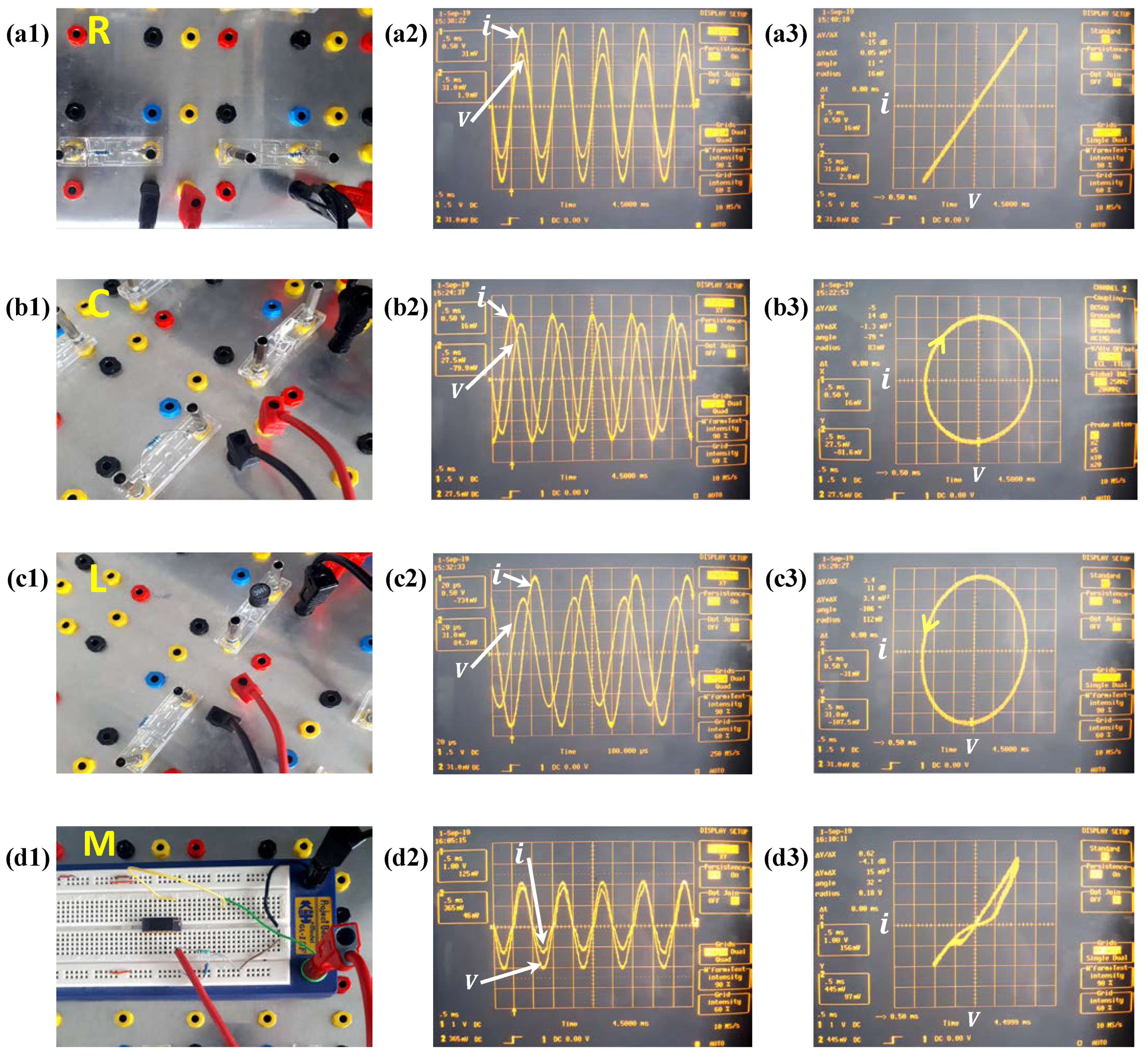

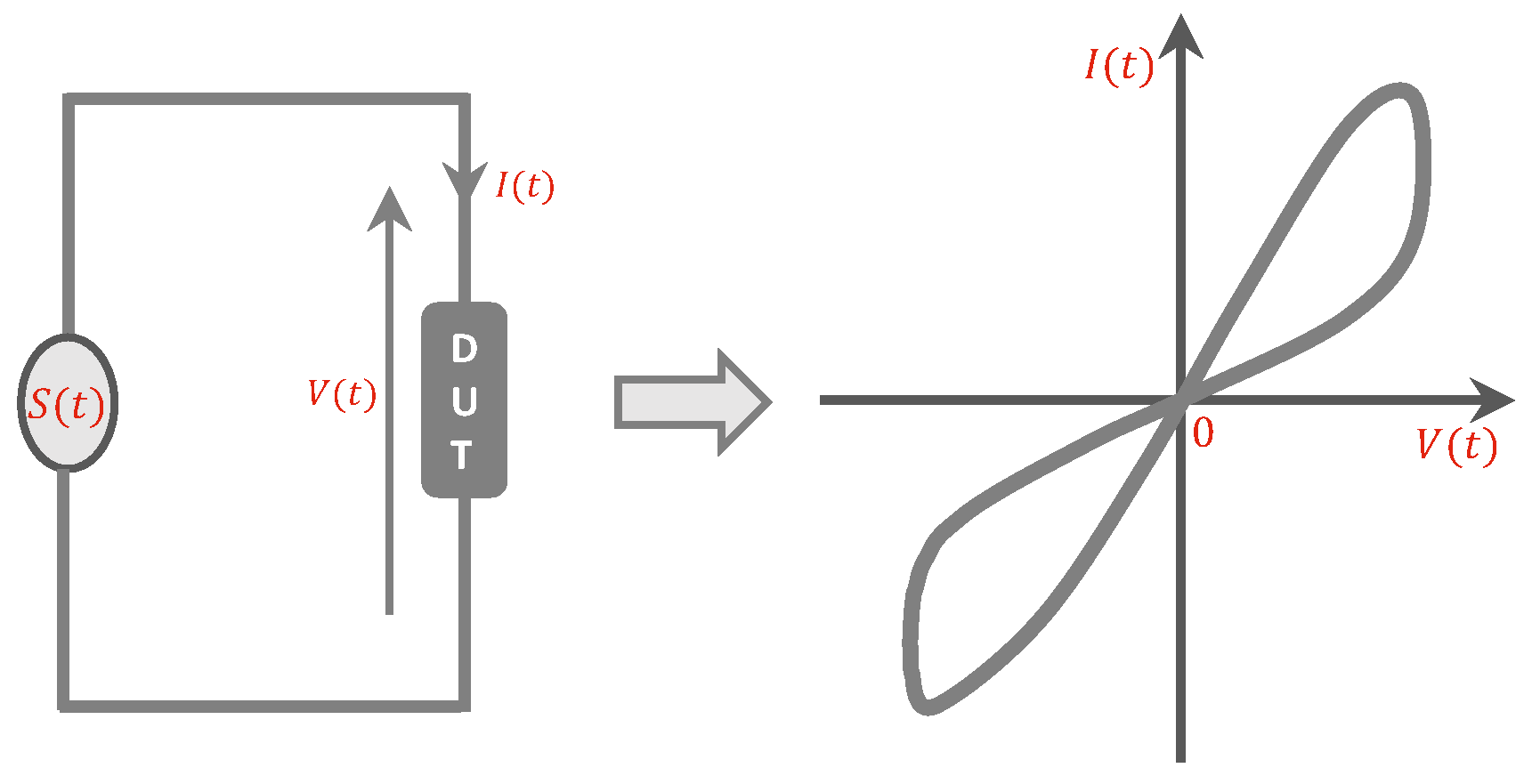


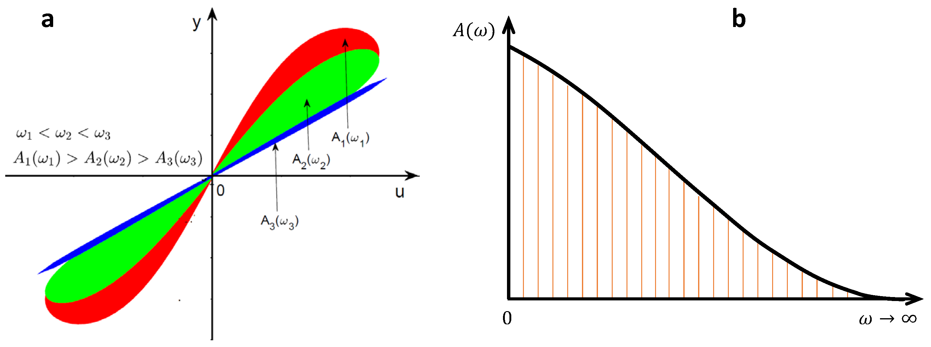
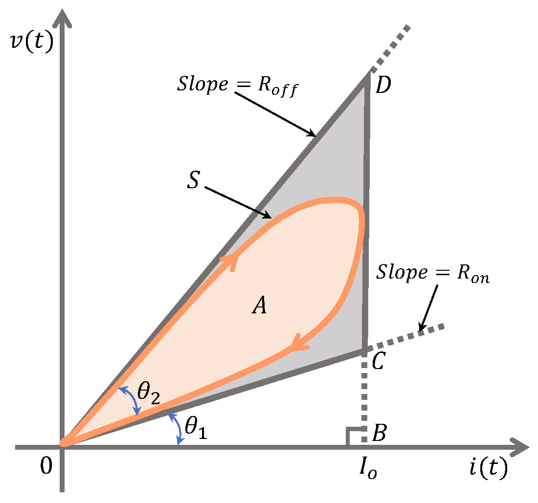


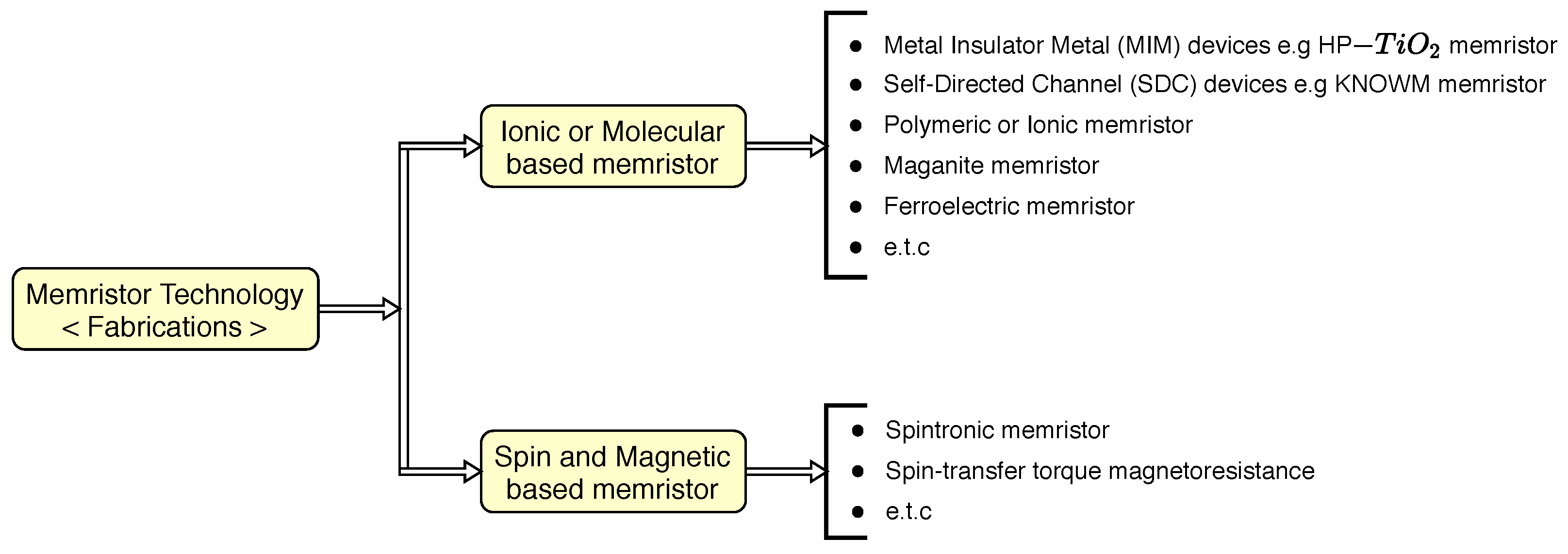
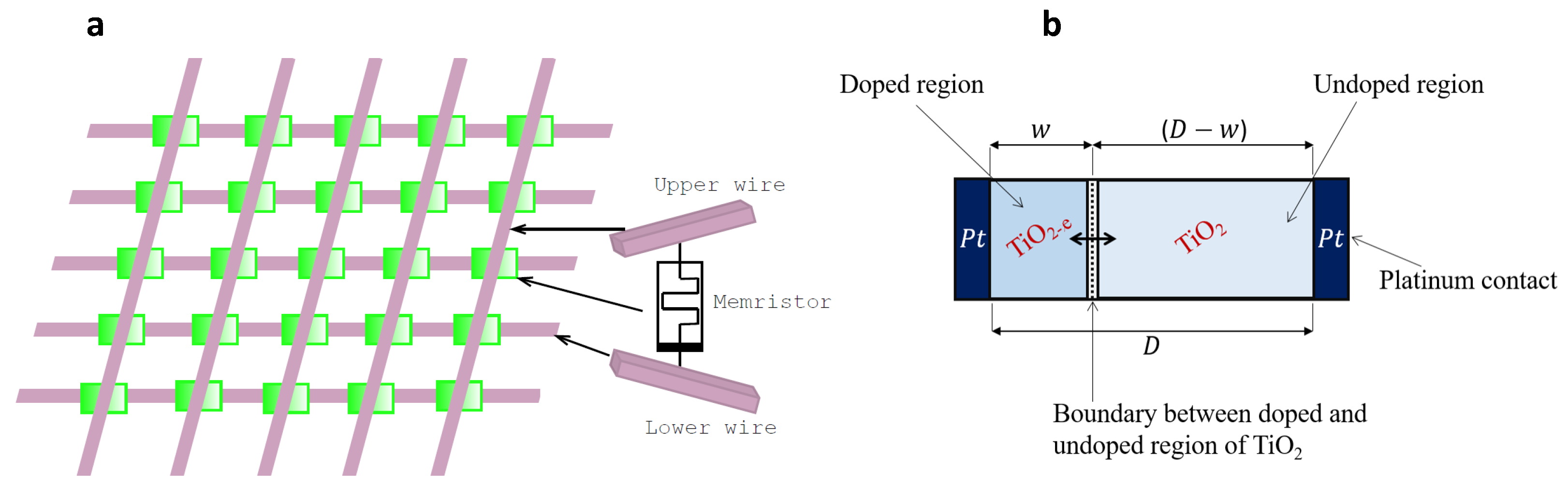

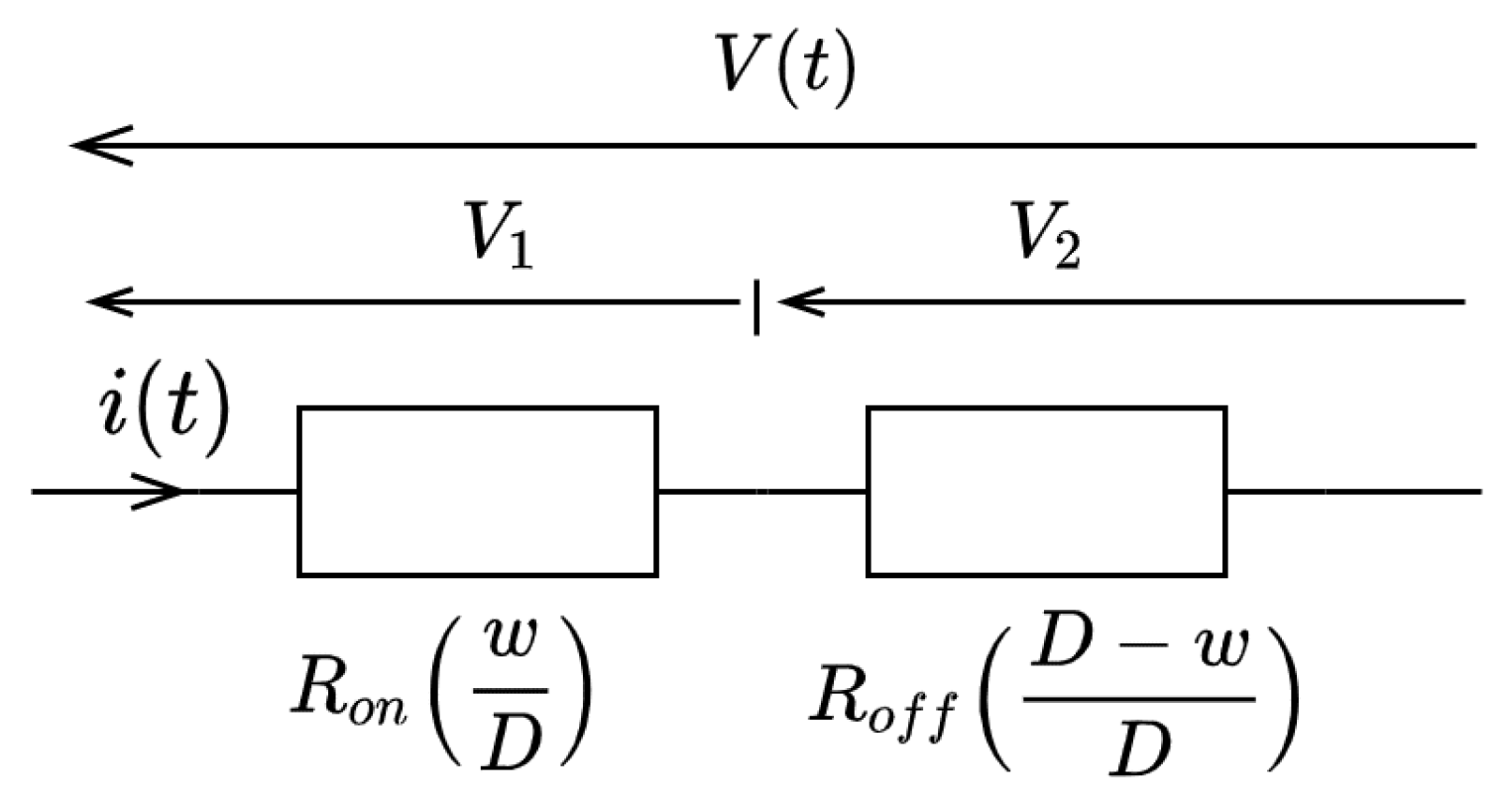


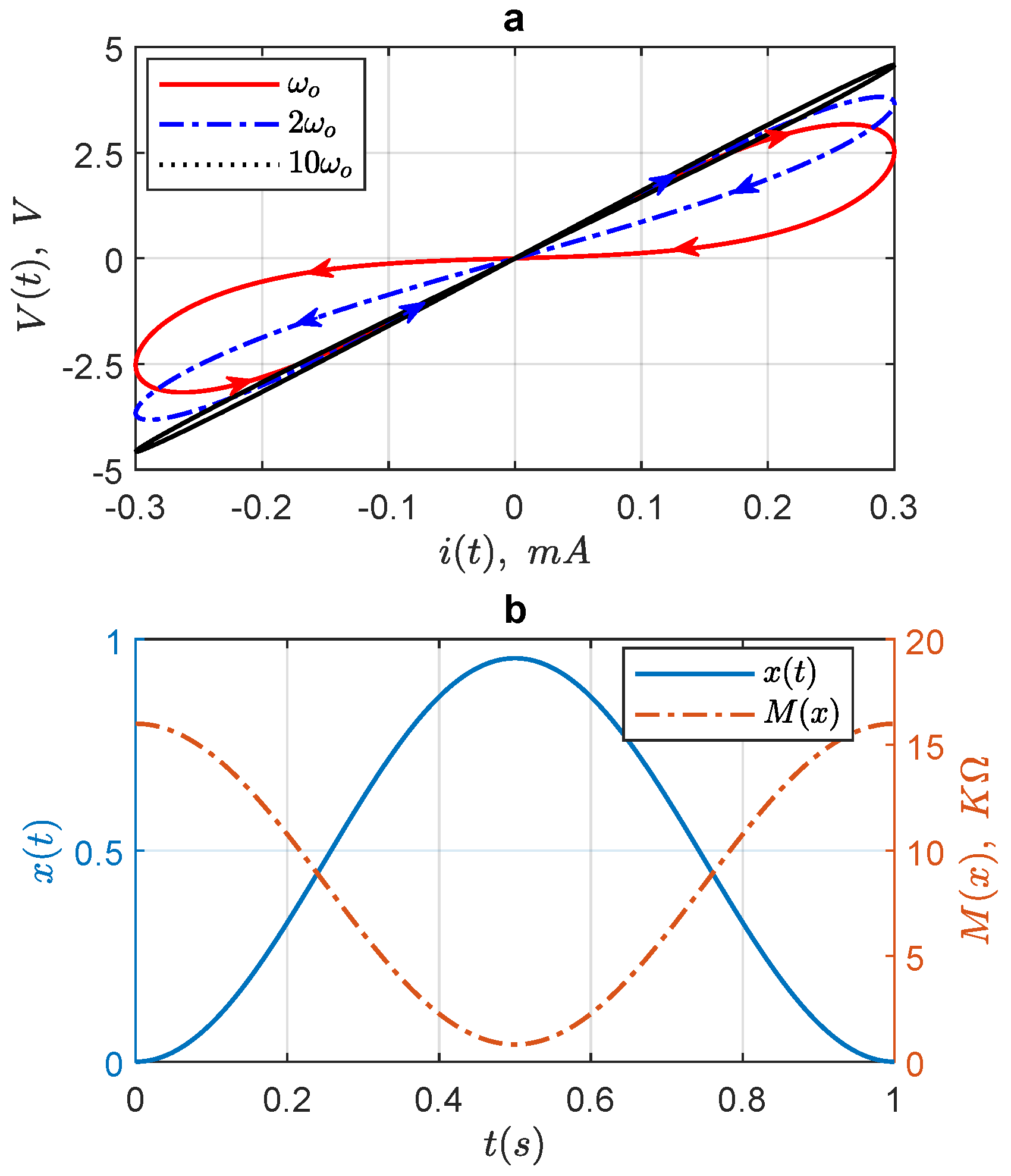

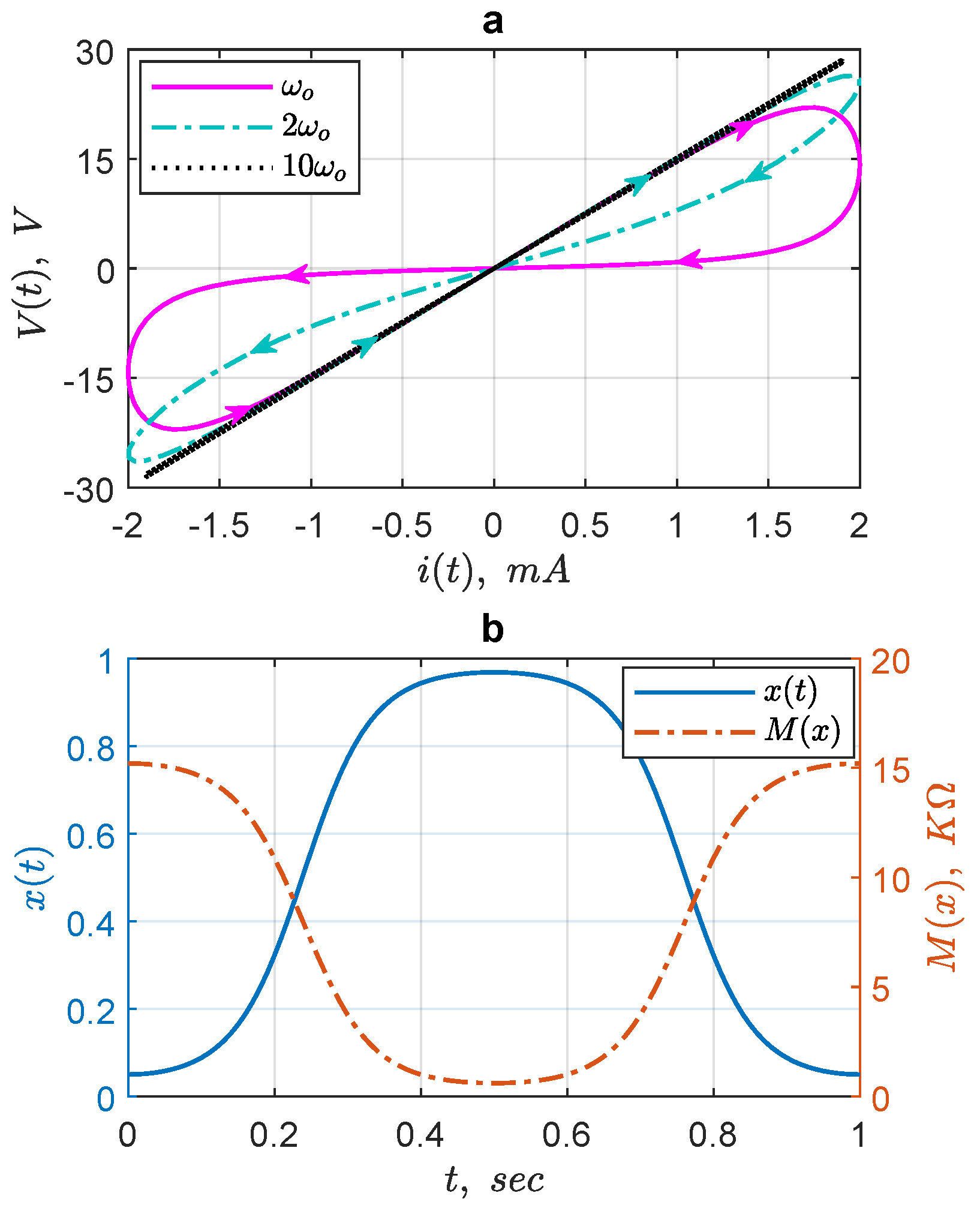

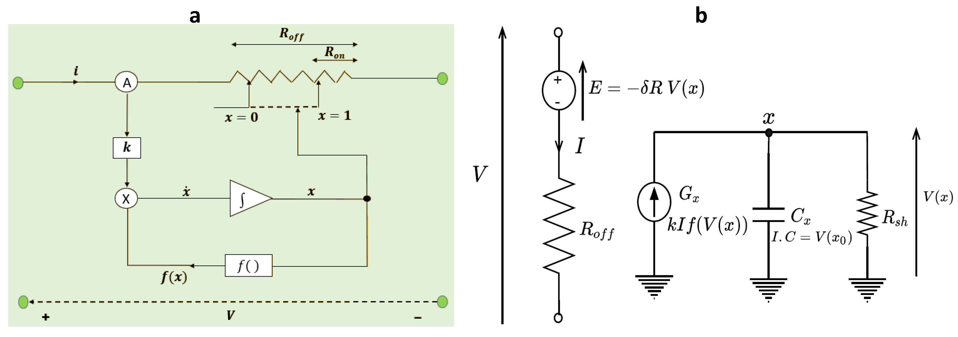
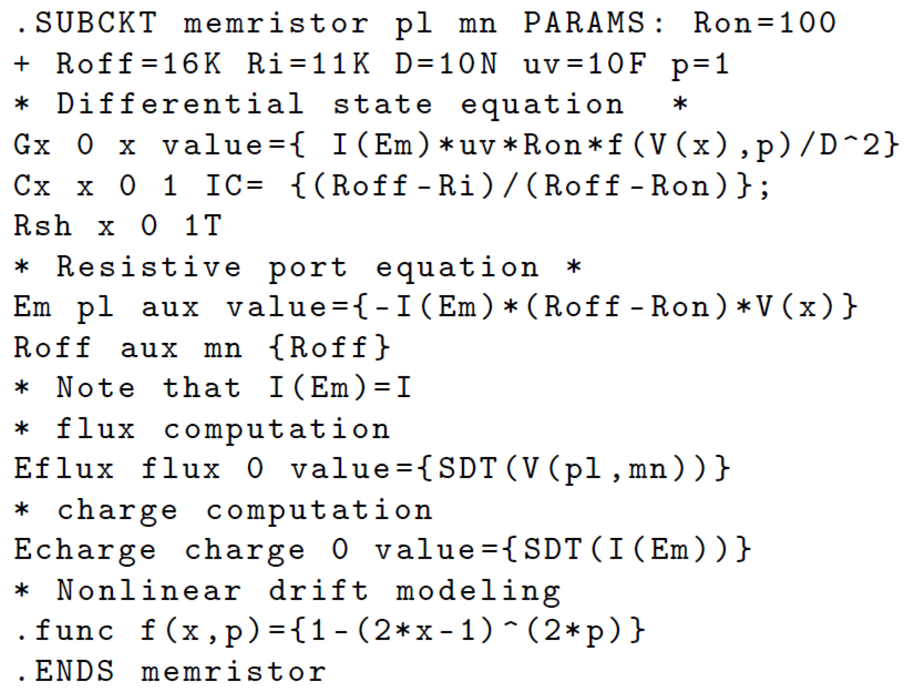


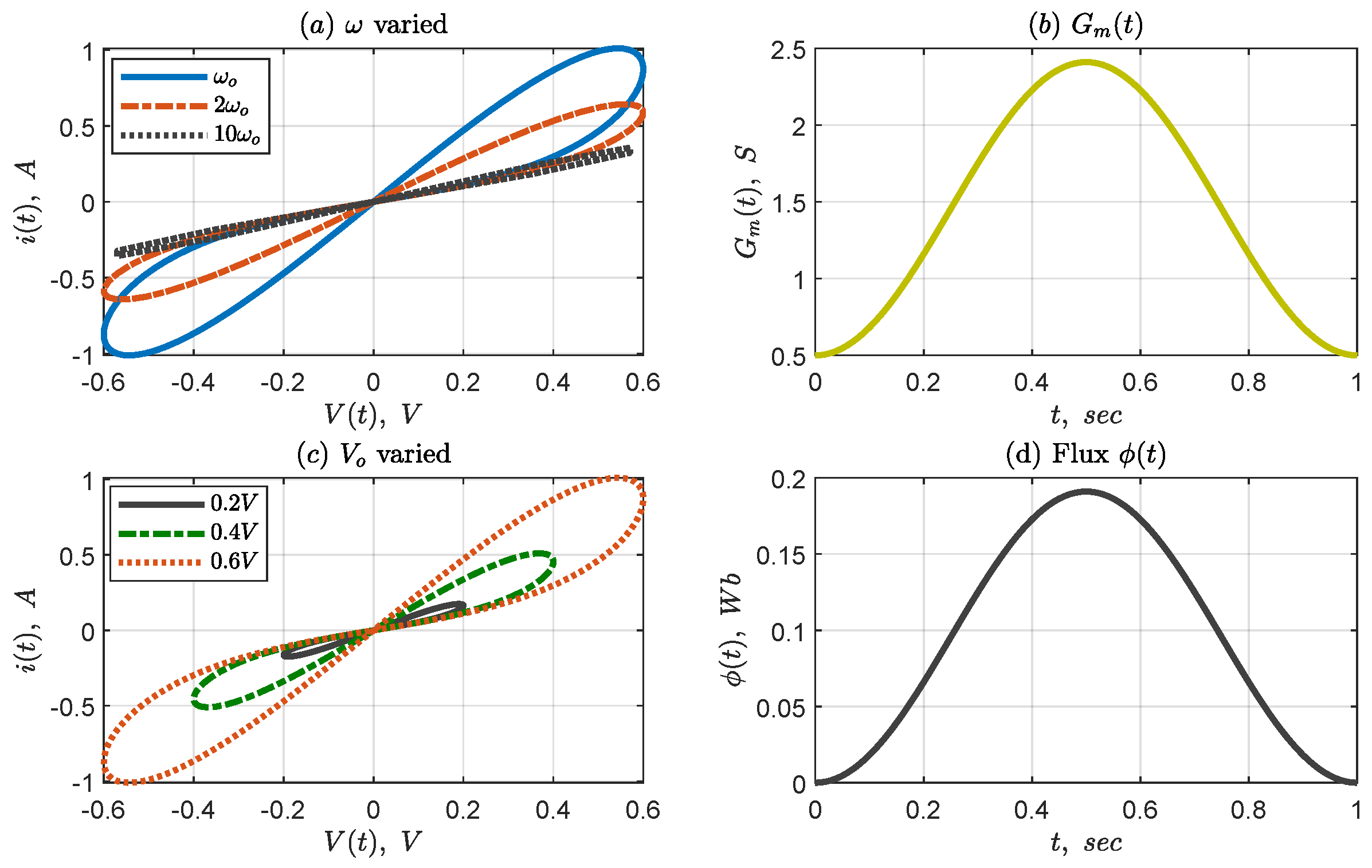
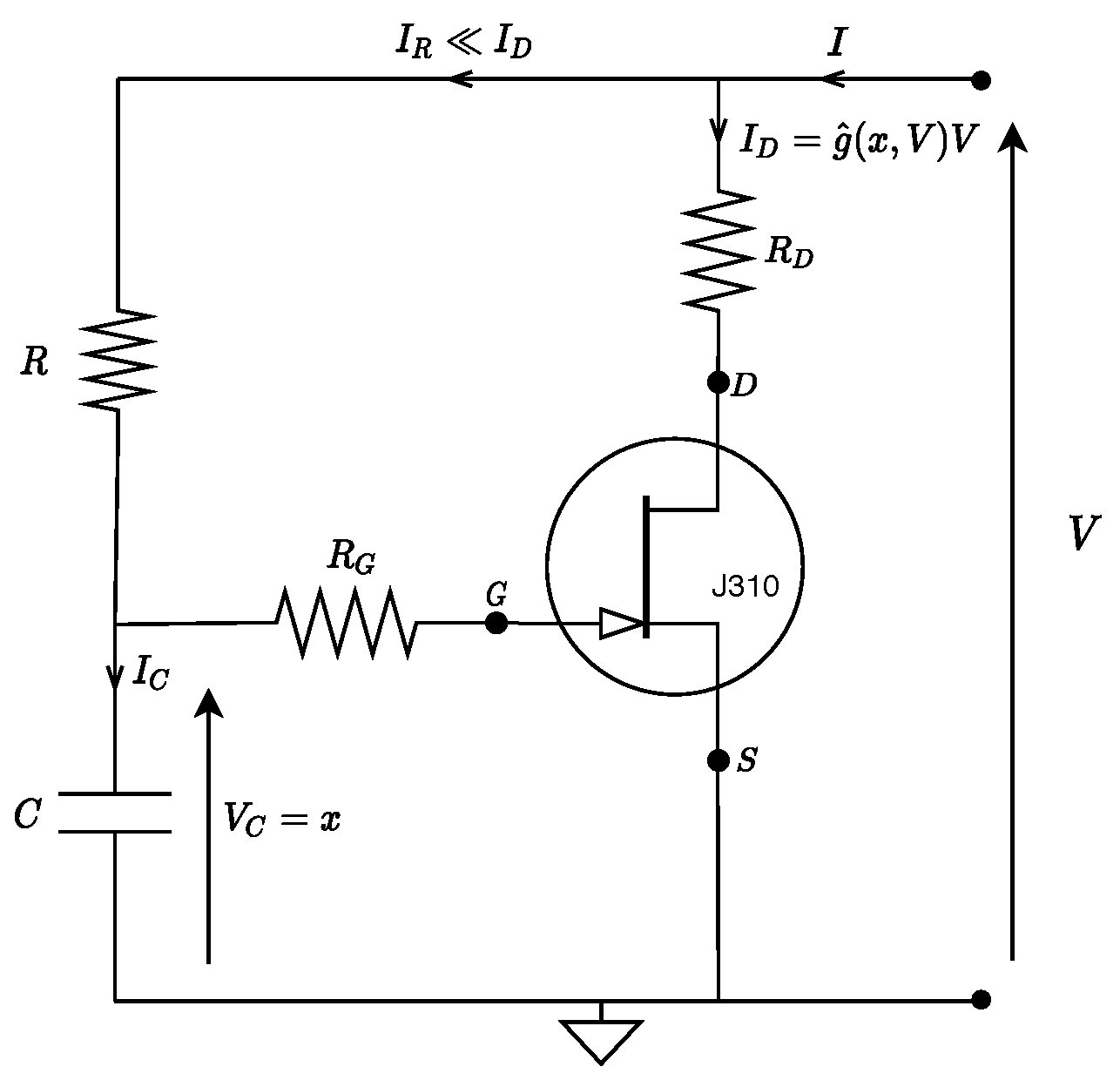
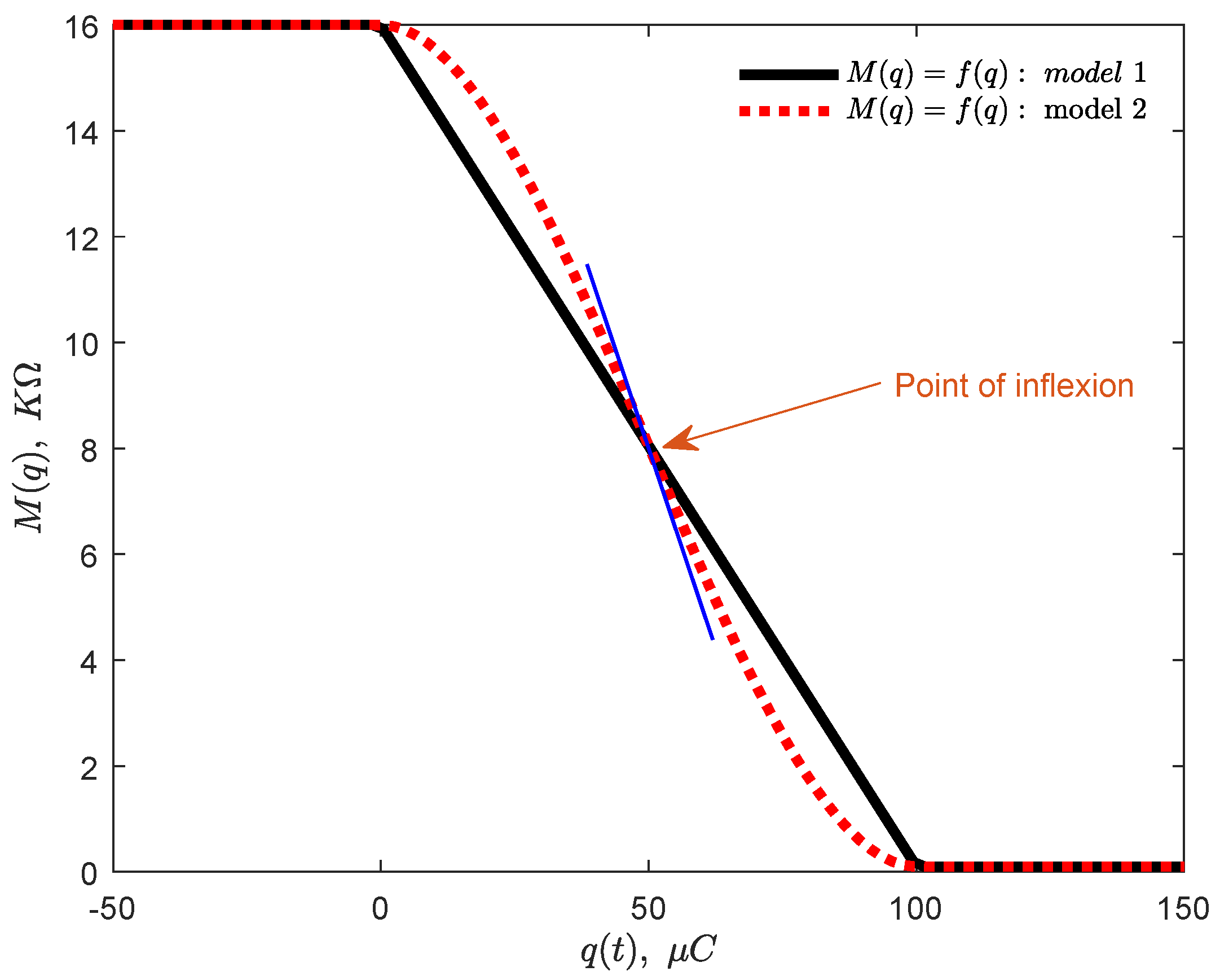
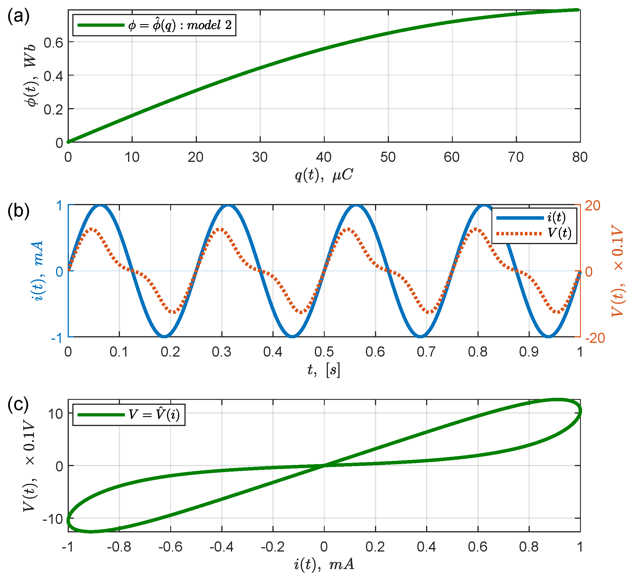


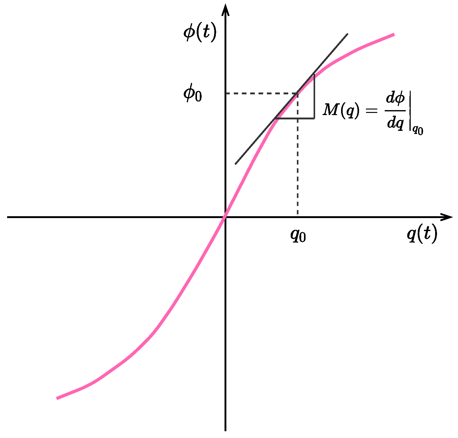
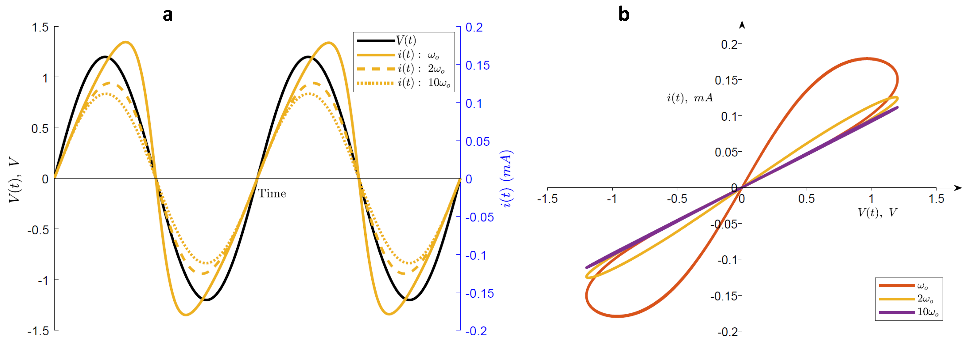
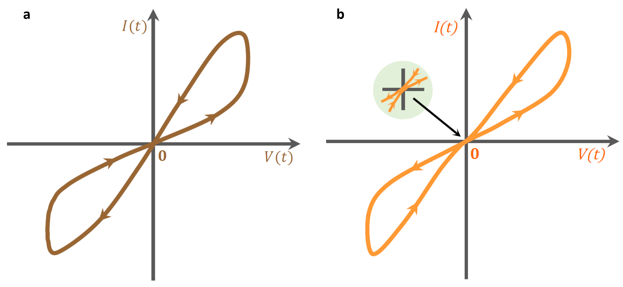
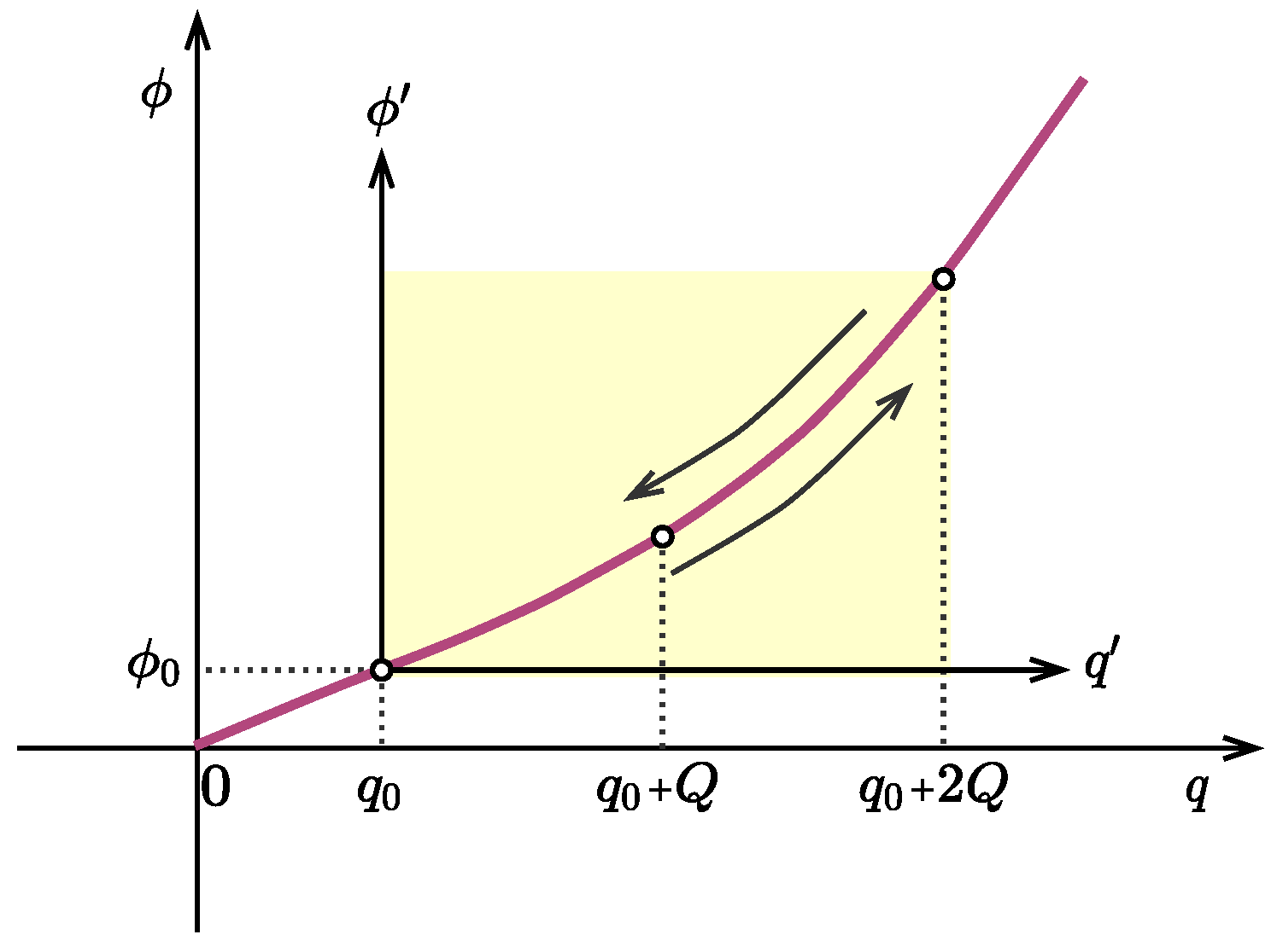
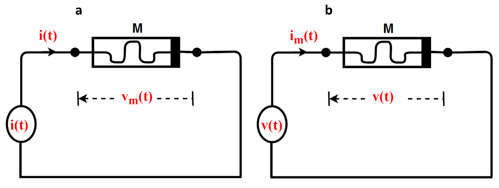
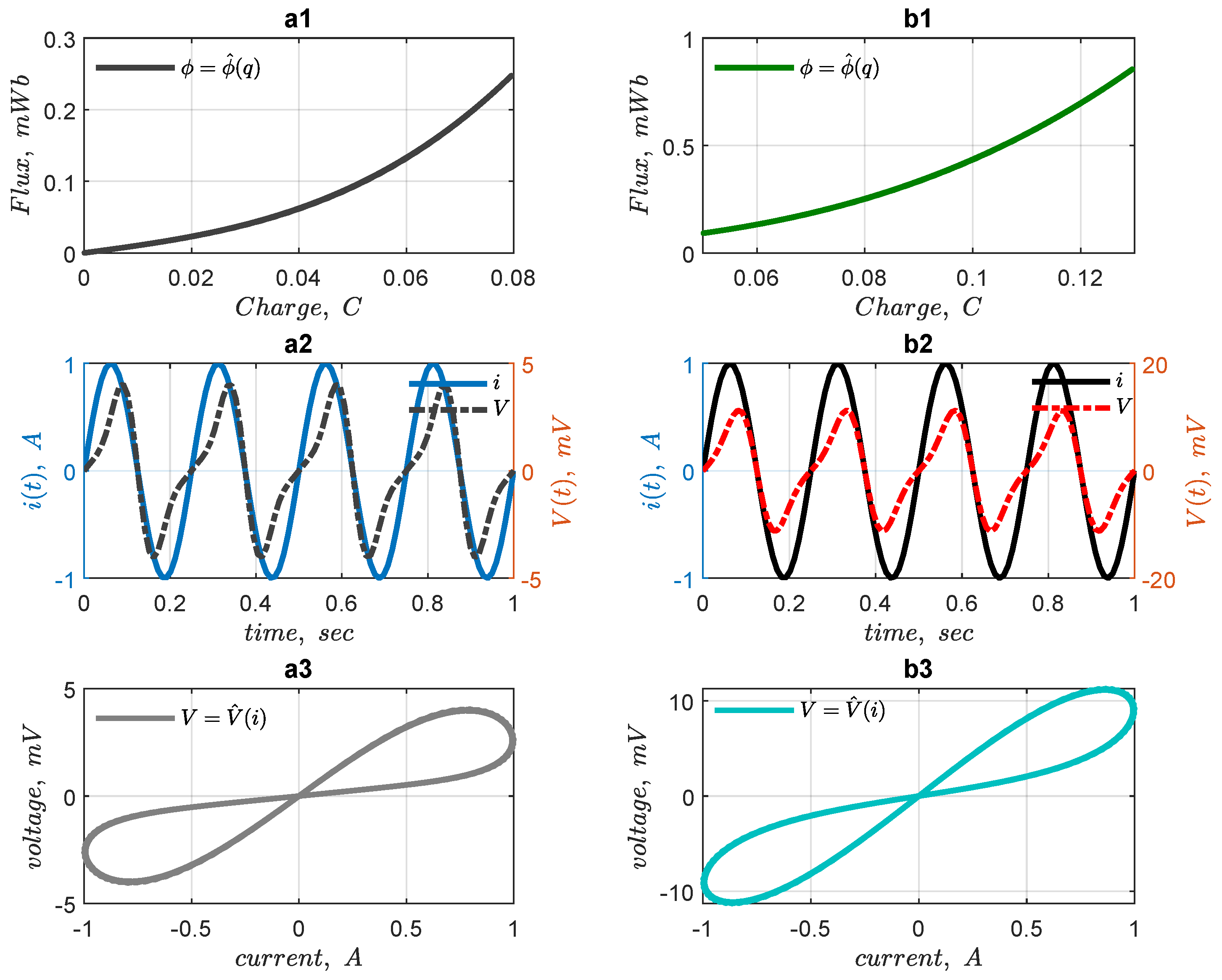
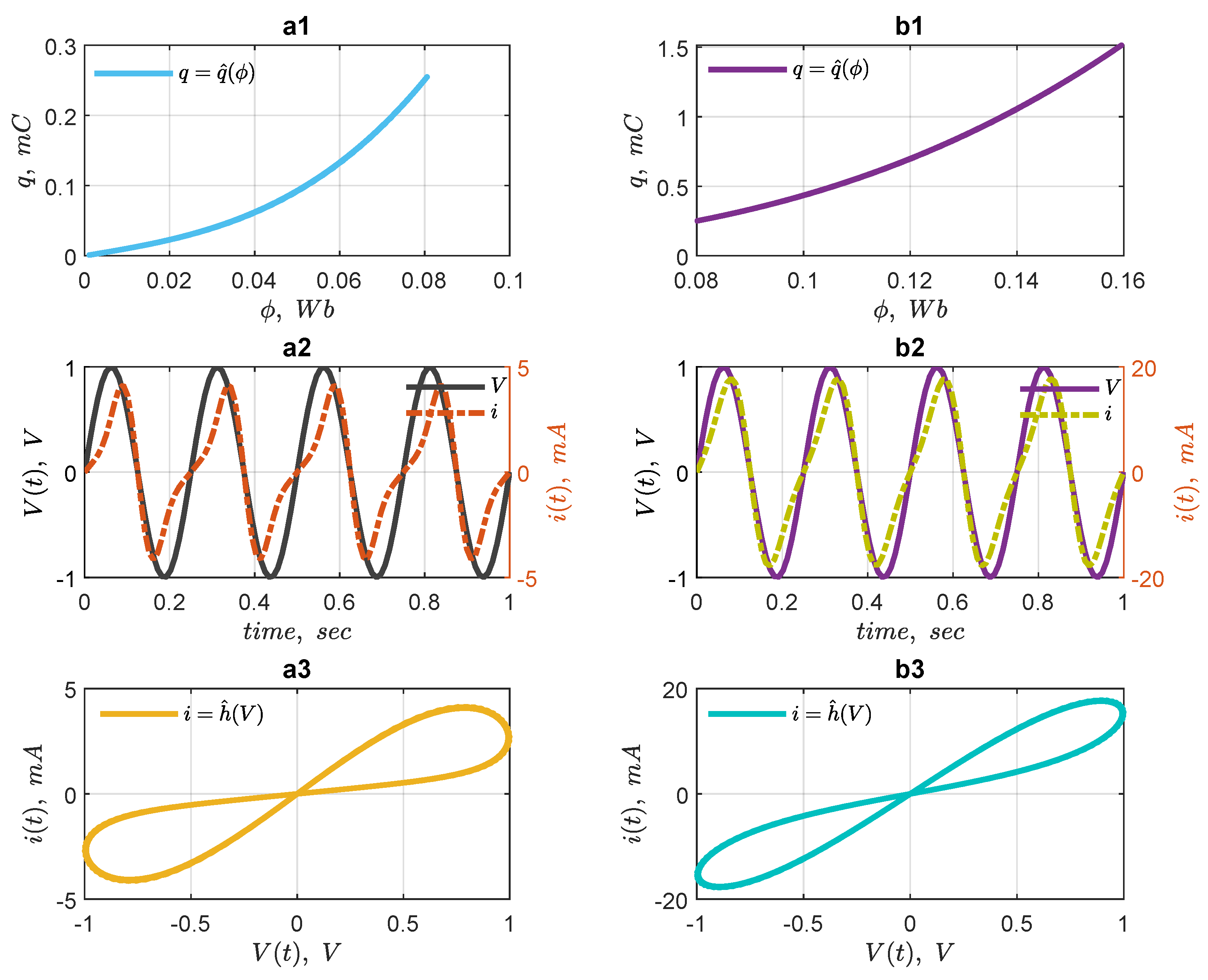
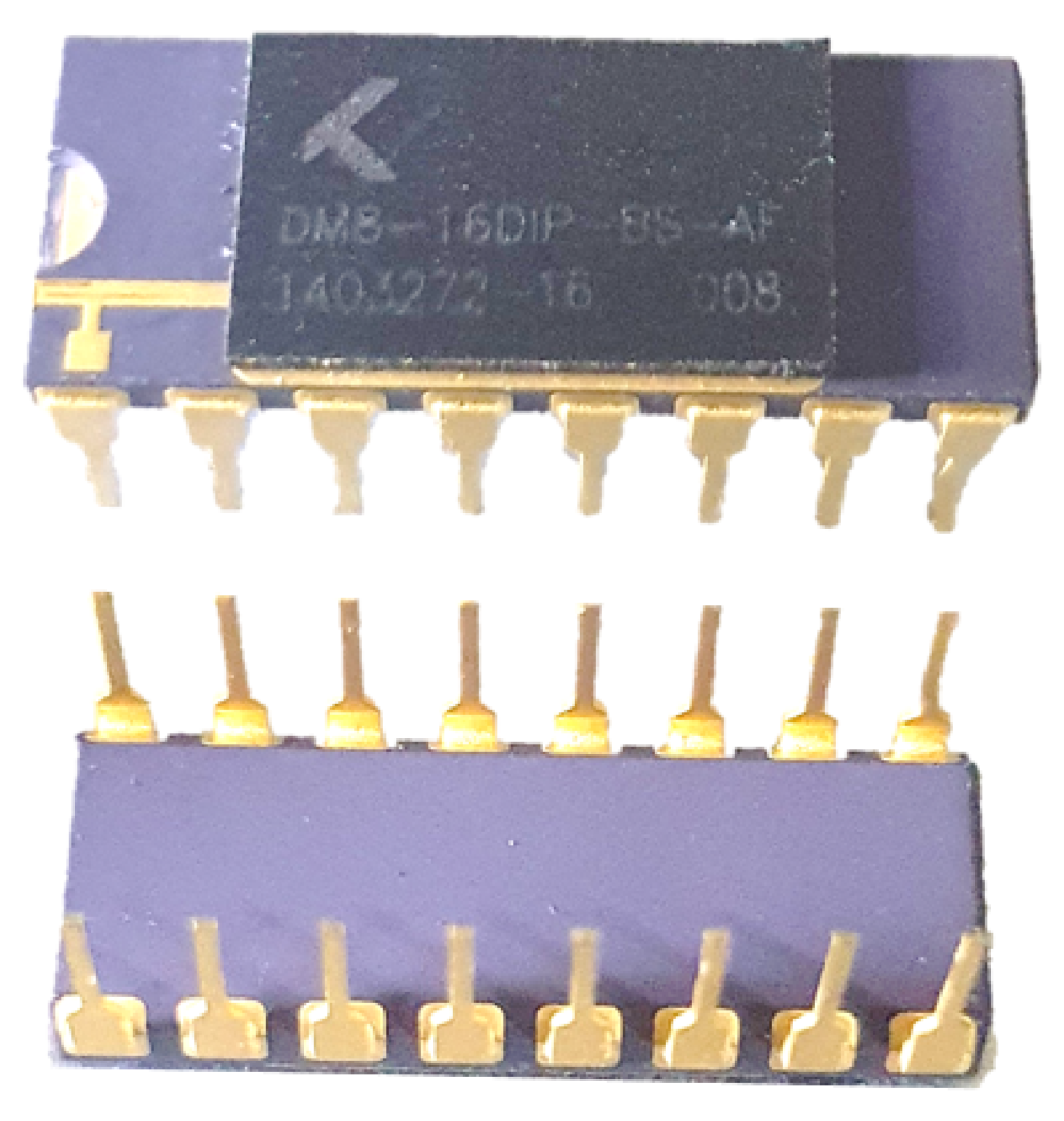
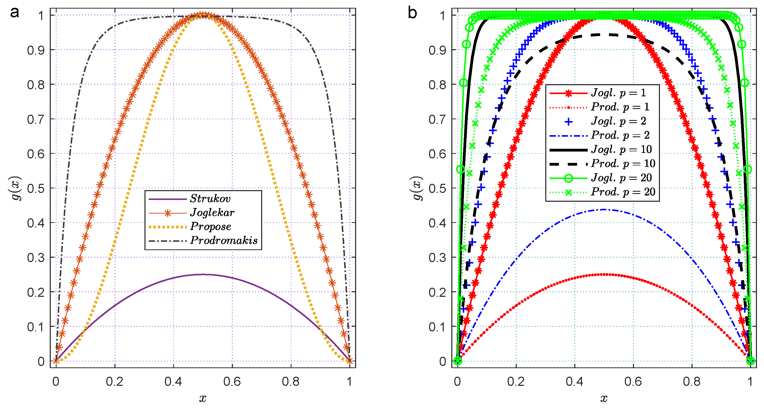
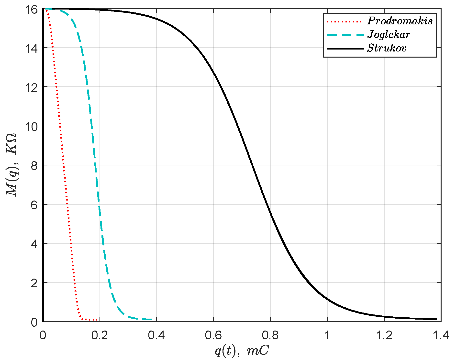
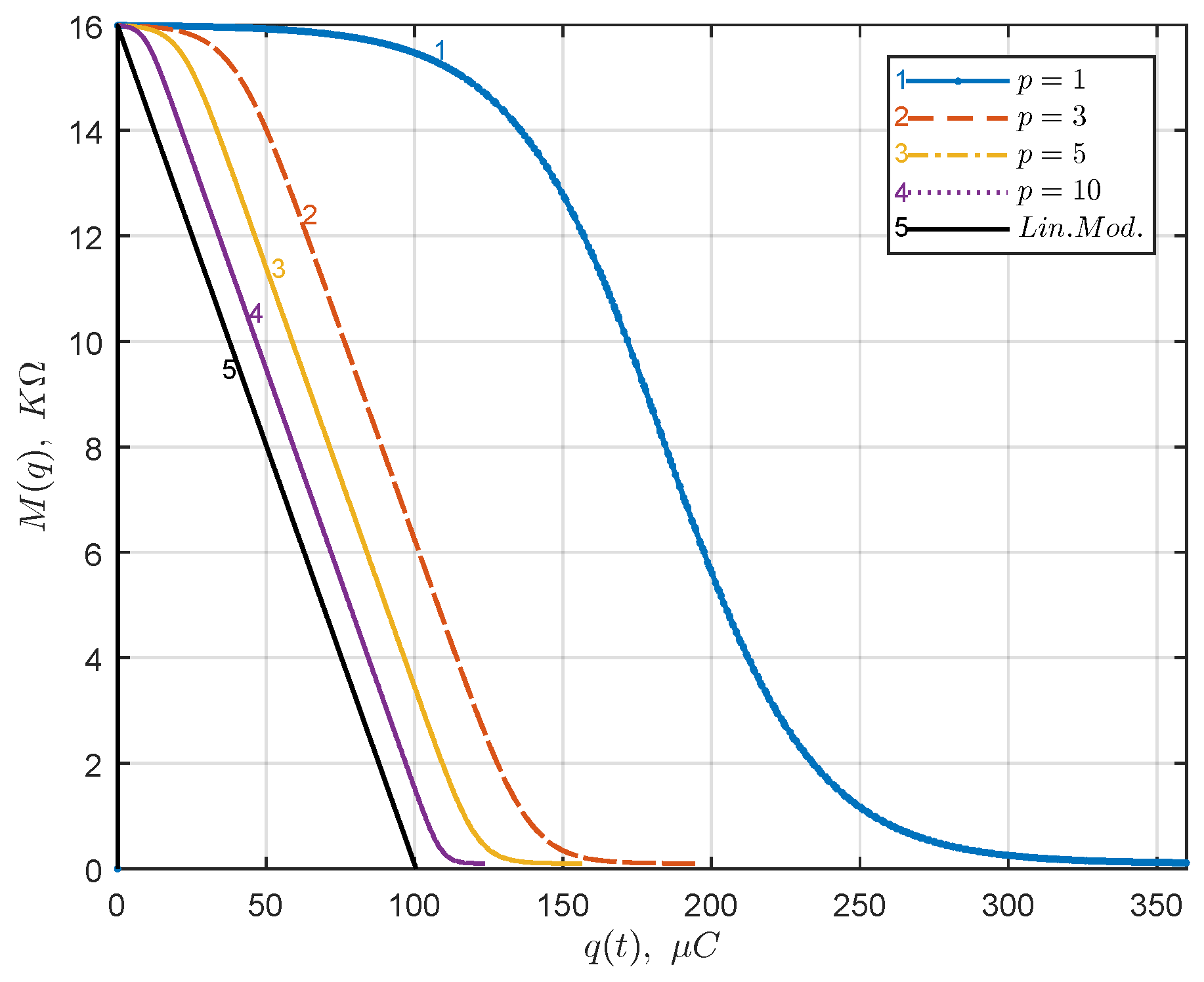
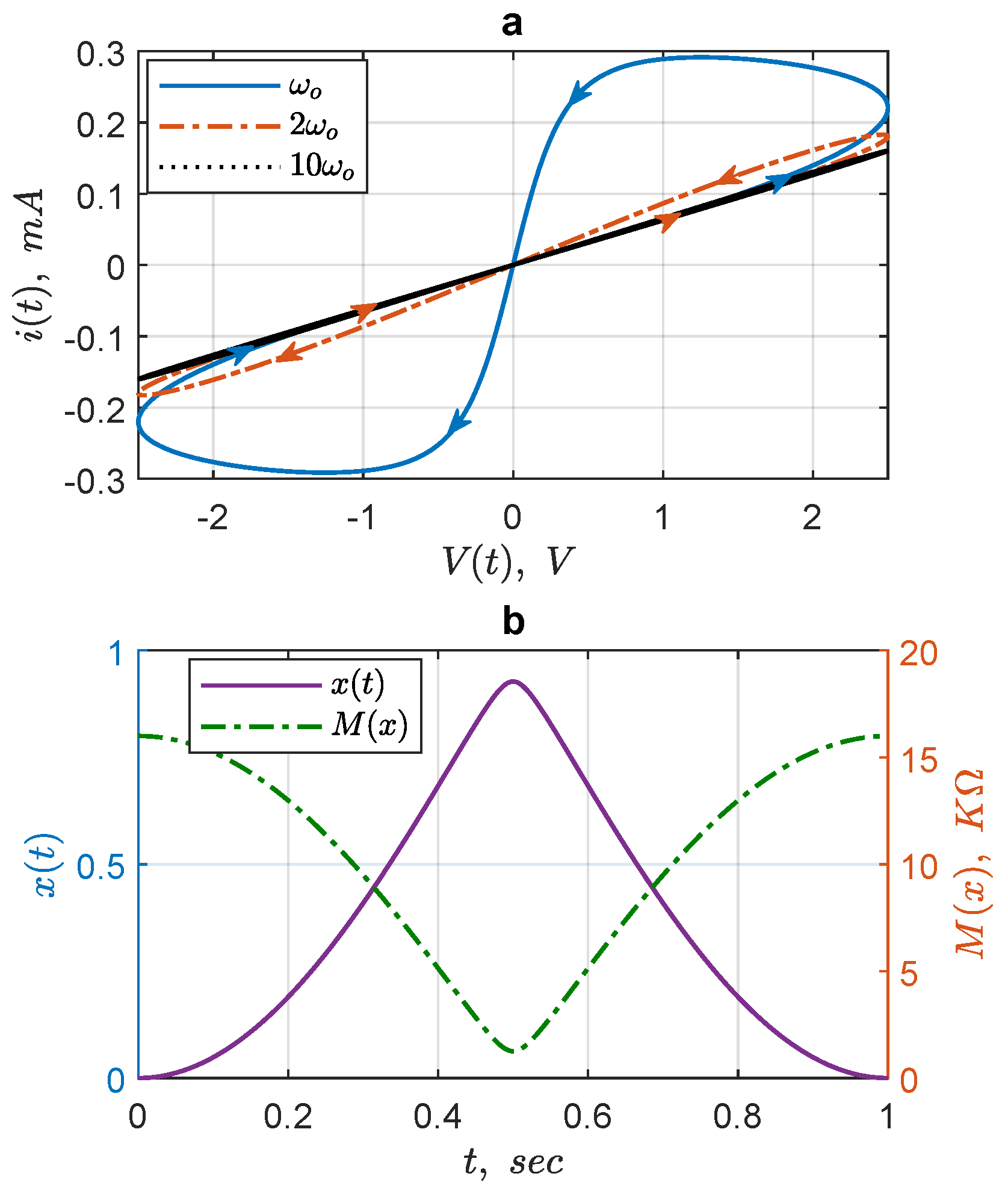
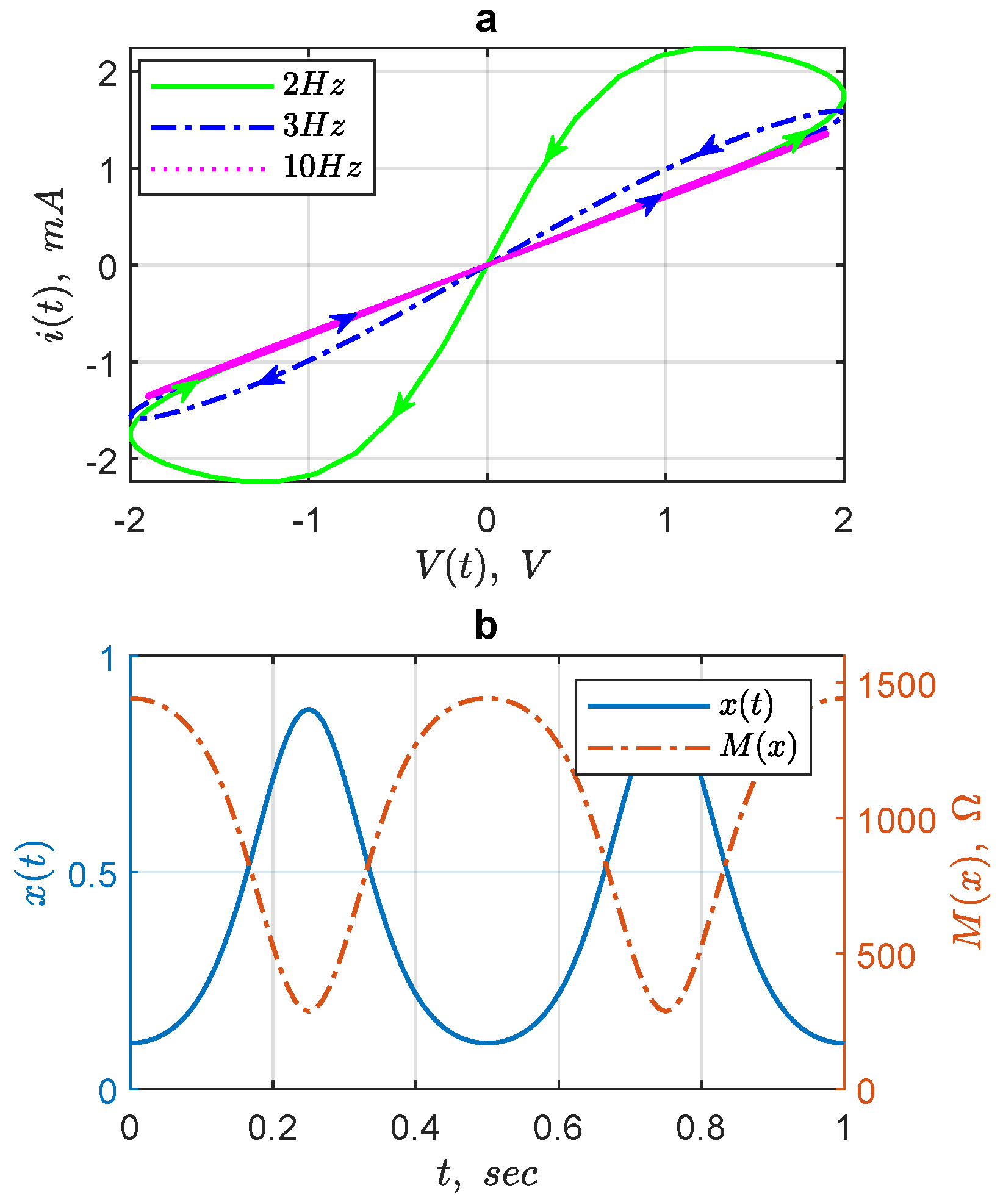
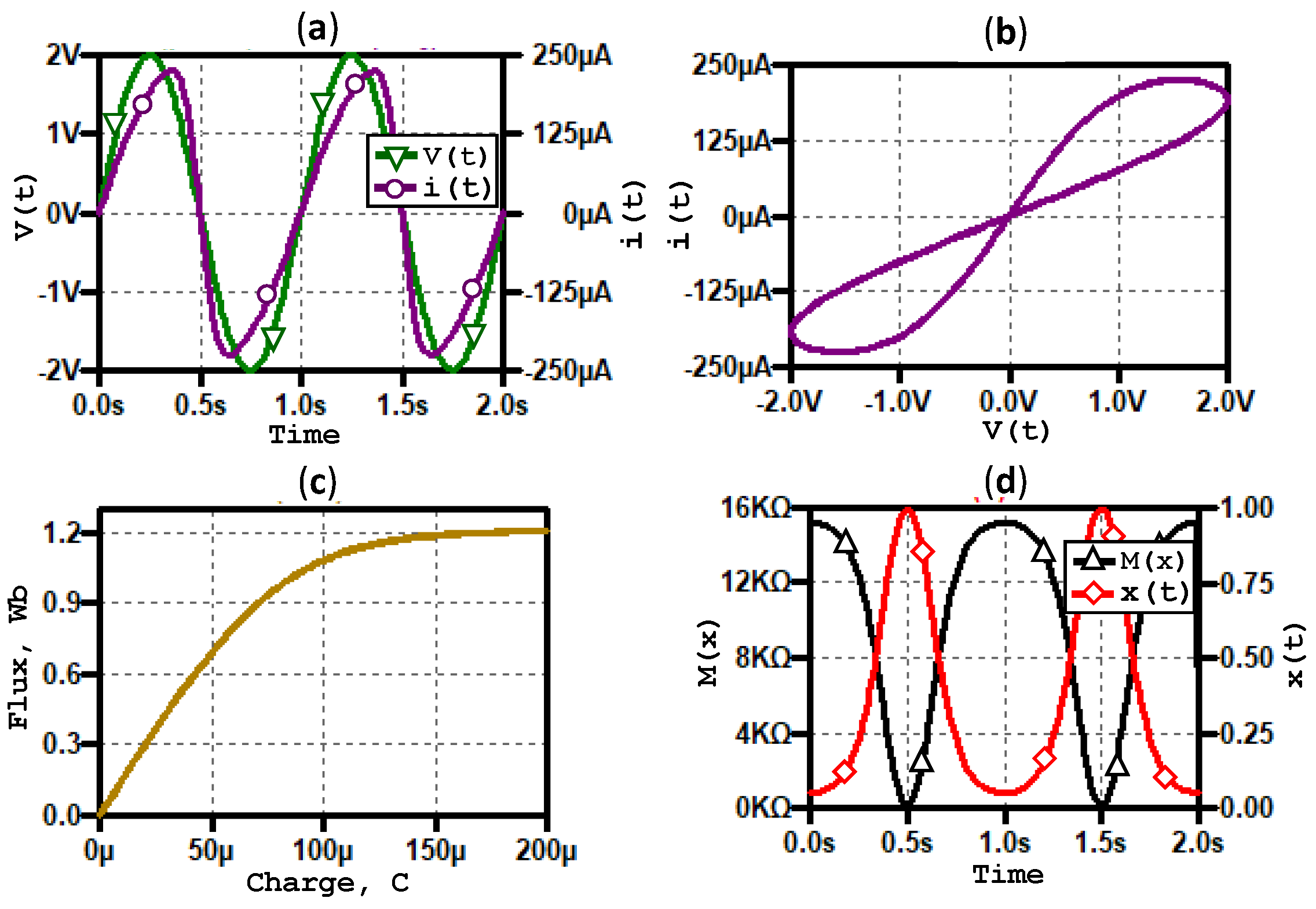
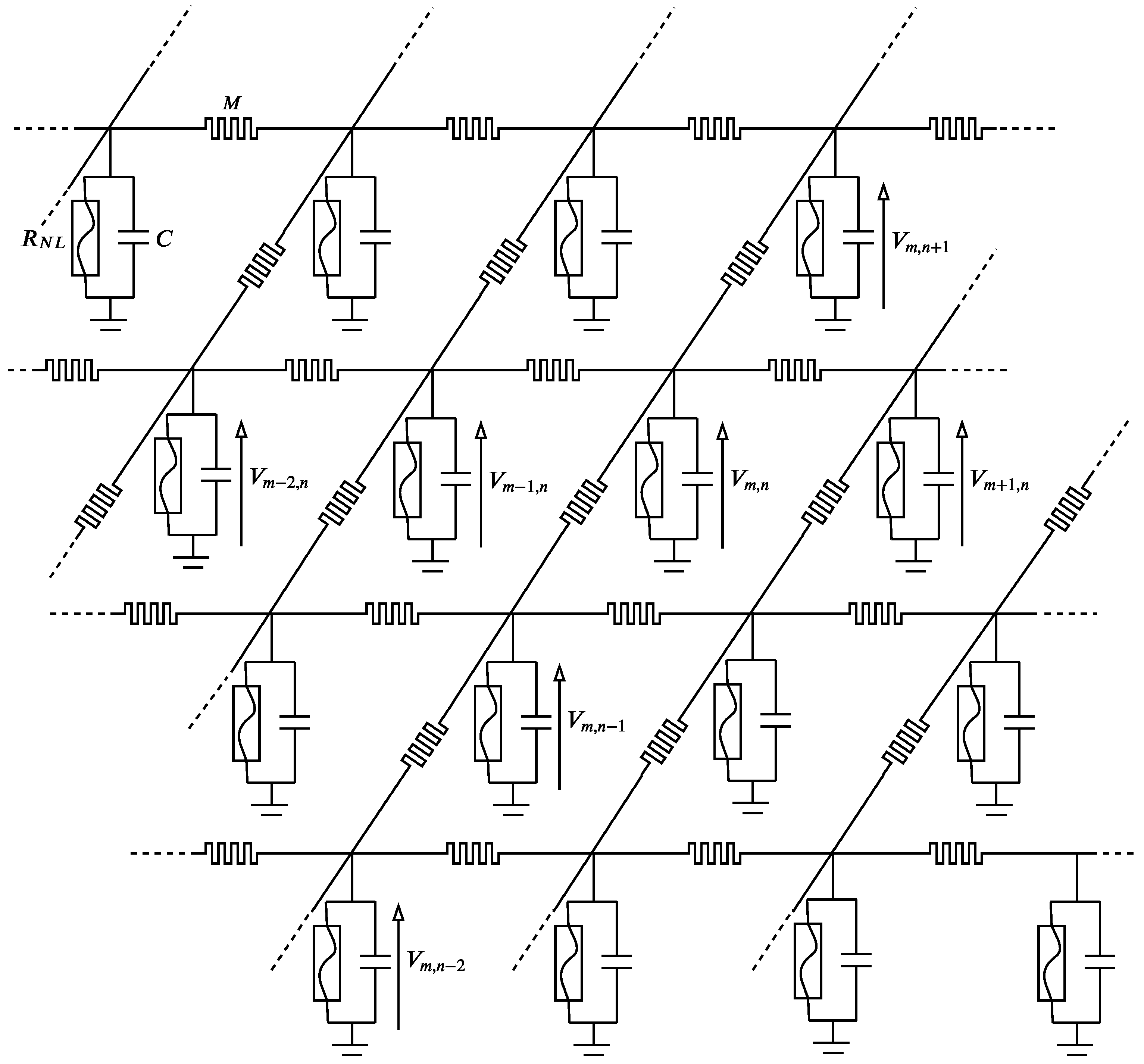