Abstract
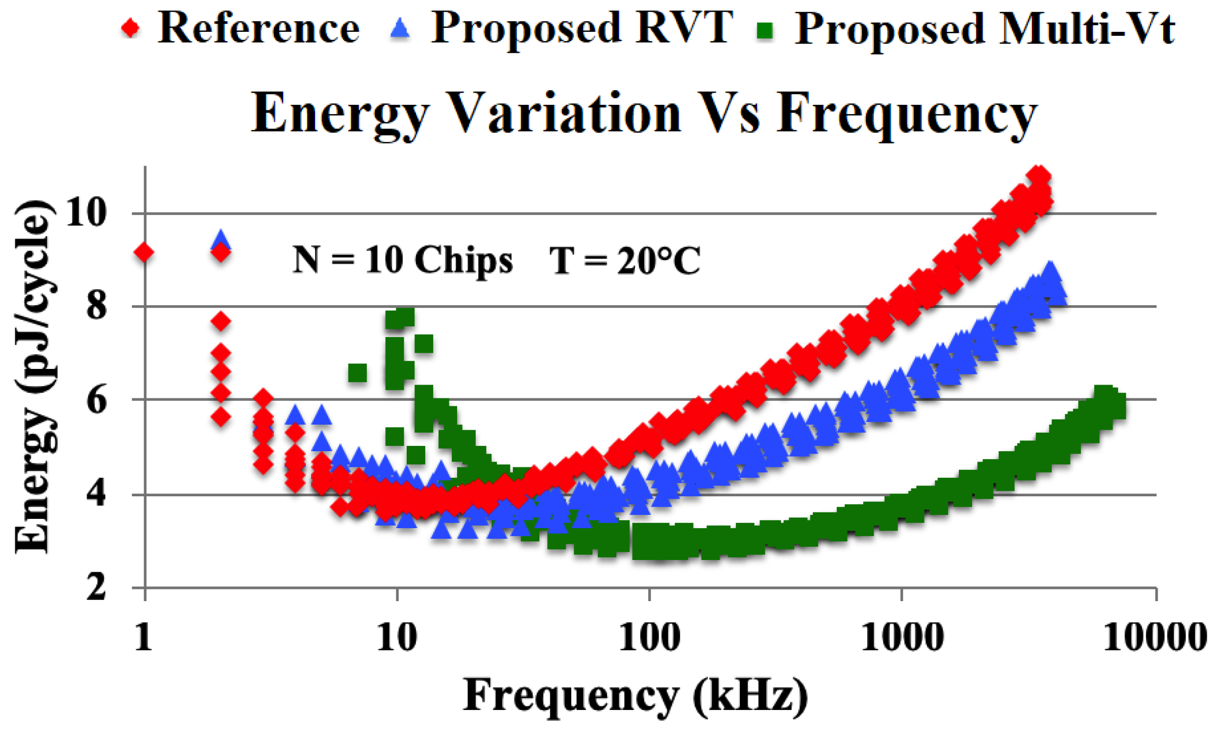
This work presents complex circuitry from subthreshold standard cell libraries created by geometric STI spacer patterning for bulk planar CMOS technology nodes. Performance/leakage granularity enhancement affords safer multi-Vt synthesis in aggressive voltage scaling schemes. Libraries are evaluated in silicon through implementation of 32-bit datapath 128-bit AES cores. Intra-die nominal temperature (20 °C) analysis reveals improvements of up to 8.65×/24% MEP-to-MEP in frequency and energy-per-cycle respectively, compared to a state-of-the-art subthreshold library. A negative temperature correlation with performance enhancement is demonstrated extending beyond the cell level and into more complex designs. MEP-to-MEP performance enhancement and energy-per-cycle reduction are demonstrated over a temperature range of 0 °C to 85 °C.
1. Introduction
The Internet-of-Things (IoT) has spawned a multitude of potential applications that demand low energy and reliable computation. Whilst most in the field agree that FinFET offers the future in silicon processing technology, mature bulk planar CMOS technology nodes still remain the most widely investigated for IoT applications, principally for their availability, low cost, low leakage and low design complexity.
Due to the electrostatic charge sharing of bulk planar devices [1] and the increase in leakage current due to the comparative scaling of the overdrive voltage [2], the natural threshold voltage may not be scaled in keeping with other dimensions in constant field scaling. The minimum energy point of a system therefore typically resides in the near- to sub-threshold regime, where the dominant geometry-dependent physical effects differ from those at nominal voltage.
Sub-threshold complex circuits up to the SoC level have recently exploded in popularity in the market, with nascent companies such as Ambiq Micro [3] cornering 80% of the fitness/smartwatch wearables sector, as well as achieving considerable adoption in medical devices. Recent filings indicate that they have shipped over 100 M units to date.
Sub-threshold operation is also currently under investigation for spiking neural networks, with energy efficient Morris–Lecar artificial neurons providing spike energies on the order of femto-joules, enabling neuromorphic circuits destined for embedded A.I. [4].
In this paper, we present subthreshold bulk planar cell libraries created from a technique that takes advantage of the underlying physics. The libraries are then used to synthesize, tape out and measure 32-bit datapath 128-bit AES cores from identical RTL to determine the performance and energy impact on complex digital circuits. Section 2 presents a brief background of the two primary physical effects being leveraged. Section 3 gives an overview of the technique upon which the work presented is based. Section 4 provides simulation results illustrating the impact of the technique on the chosen technology node. Section 5 outlines the synthesis methodology and provides critical metrics for the final core designs. Section 6 presents the measured silicon results. Section 7 discusses the merits and limitations of the work presented as well as considerations to be made when implementing the technique. Section 8 concludes the work.
2. Background
In order to prevent drain induced barrier lowering (DIBL) and the short channel effect (SCE) in superthreshold operation, fabrication houses perform an additional HALO implantation stage to increase the channel dopant density adjacent to the source/drain regions. The lower biasing in subthreshold operation vastly reduces the impact of these effects on the drain current. In minimum length devices, this leaves a higher dopant density in the centre of the channel where the HALO implants converge. Increasing the length of the device serves to lower the overlap of this implant stage, lowering the overall dopant density and decreasing the threshold voltage (). This condition is known as the reverse short channel effect (RSCE). The authors of [5] observed 16 mV/decade improvements in the subthreshold slope leading to 10.4% delay improvements by RSCE optimal sizing. This resulted in 39%/41.2% power/energy savings compared to a superthreshold library, primarily driven by a leakage energy reduction. However, these results were not derived from complex circuitry.
Shallow trench isolation (STI) was widely adopted in the 1980s to overcome the density restrictions of local oxidation of silicon (LOCOS). Polysilicon gate material has a tendency to ‘claw-back’ from drawn dimensions. As such, minimum overlap rules with the thick field oxide are enforced to ensure active diffusion areas are sufficiently covered. As the isolation material is also , a fringing field permeates through the sidewall and into the channel, depleting the channel deeper and thus lowering . The threshold voltage may therefore be derived as [6]:
where the fringing factor F is:
where is the flat band voltage, is the surface potential (equivalent to 2 kT/q(ln(/)) at the point of inversion), is the electric field in the gate oxide, is the gate oxide thickness, W is the device width and is the field oxide thickness. The proportion of the channel influenced by the fringing field increases as the device width decreases. This phenomenon is therefore known as the inverse narrow width effect (INWE). Subthreshold cell library design has thus far focused on quantized minimum width fingers. Whilst this at first seems logical, it is important to note that this strategy increases the leakage current greater than the drive current, degrading the Ion/Ioff ratio and deteriorating the performance-to-energy metric. The authors of [7] observed a 72% reduction in simulated energy-delay product by INWE optimal sizing of minimum width fingers. The authors of [8] elaborated further by synthesizing 32-bit IcyFlex processors and demonstrating power reductions of up to 5× compared to a superthreshold library during post-parasitic extracted simulation. None of the aforementioned studies were corroborated in silicon.
3. Proposed Libraries
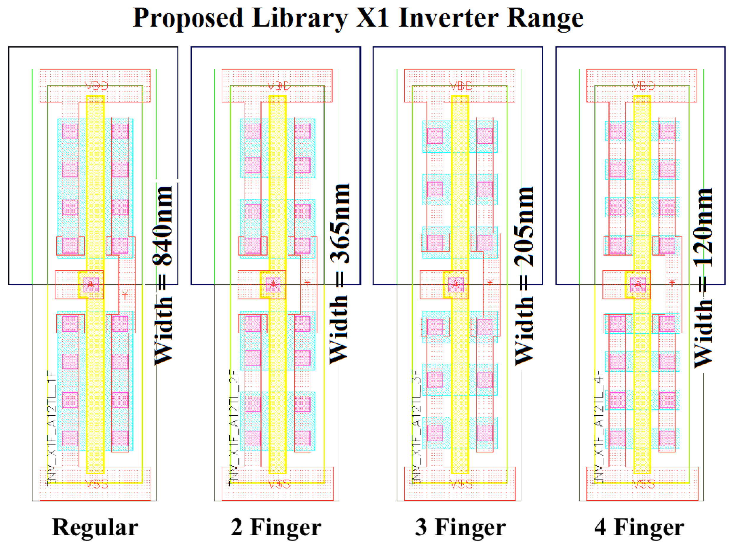
Ref. [9] proposed an unconventional layout technique that takes advantage of the fringing field by geometrically introducing STI spacers into a maximised diffusion area. Application of this technique to a 12-track (2.4 μm) X1 inverter cell in a commercial 65 nm LP process is shown in Figure 1.
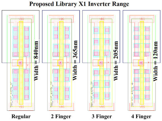
Figure 1.
INVX1 proposed cells.
Silicon results from ring oscillators revealed frequency improvements of up to 2.77× due to higher drive currents and lower gate capacitances. The contributions for these ranged from 83–96% current increase to 4–17% capacitance reduction depending on cell type and finger count. Frequency enhancement was measured up to supply voltages of 800 mV for all finger variations with a maximum 5% performance penalty at nominal voltage (1.2 V) suggesting enhanced performance in Dynamic Voltage and Frequency Scaling (DVFS) schemes. The frequency uplift was higher at lower temperatures, compensating for temperature inversion and indicating additional temperature stability in the subthreshold regime. Interestingly, the measured results revealed that the performance-to-leakage metric improved with initial fingering (2 fingers) and that the metric degraded with an increase in fingers (decrease in width) and decrease in temperature. The gates always displayed a progressive and logical increase in performance as the number of fingers was increased across the entire supply voltage range, indicating a deterministic level of controllability in the process of creating a performance range from the cell characteristics. This suggests a finer granularity for Multi-Vt synthesis and applicability to ultra-wide dynamic voltage scaling (UWDVS) without disproportionate path timing errors.
This work builds on the aforementioned study by application of the proposed geometric STI spacer technique to full subthreshold cell libraries in both Low Threshold Voltage (LVT) and Regular Threshold Voltage (RVT) in a commercial 65 nm LP (Low Power) process. Confirmatory simulations on the claims of the underlying physical effects were performed by parametric geometry sweeps in the chosen technology node. To ensure correct interpretation of the technique by synthesis tools, 128-bit AES cores were synthesized in a commercial EDA synthesis workflow and committed to silicon. Intra-die measurements under various operating conditions were then taken to determine whether the performance and energy claims of the aforementioned study are manifest in more complex digital circuitry.
4. Physical Design
4.1. Current Optimisation
Geometric sweeping of the chosen technology node was performed at subthreshold voltages across SS/TT/FF corners, both VT types and both device types to determine susceptibility to the technique. Figure 2 shows the typical corner response for the RVT PMOS device. The threshold voltage roll-off as a result of SCE highlights the danger of minimum length sizing in the subthreshold. RSCE pushed the optimal geometry to a higher device length and INWE pushed the optimal geometry to a lower device width. Cumulative results revealed subthreshold Ion/Ioff ratios in the typical corner of 1500/2500 for LVT/RVT, respectively, suggesting that RVT was the superior choice for energy critical applications. Both RSCE and INWE optimisation proved to have a greater impact on LVT devices due to the balance of HALO dopant densities with the background channel in the chosen technology. Corner analysis revealed RSCE greater in the slow corner and INWE greater in the fast corner. This is congruent with the notion that dopant depth forms part of the global variation corner, with high surface dopant density forming part of the slow corner profile and low surface dopant density forming part of the fast corner profile.
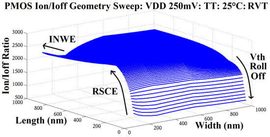
Figure 2.
Simulated Ion/Ioff Geometric Sweep.
4.2. Capacitance
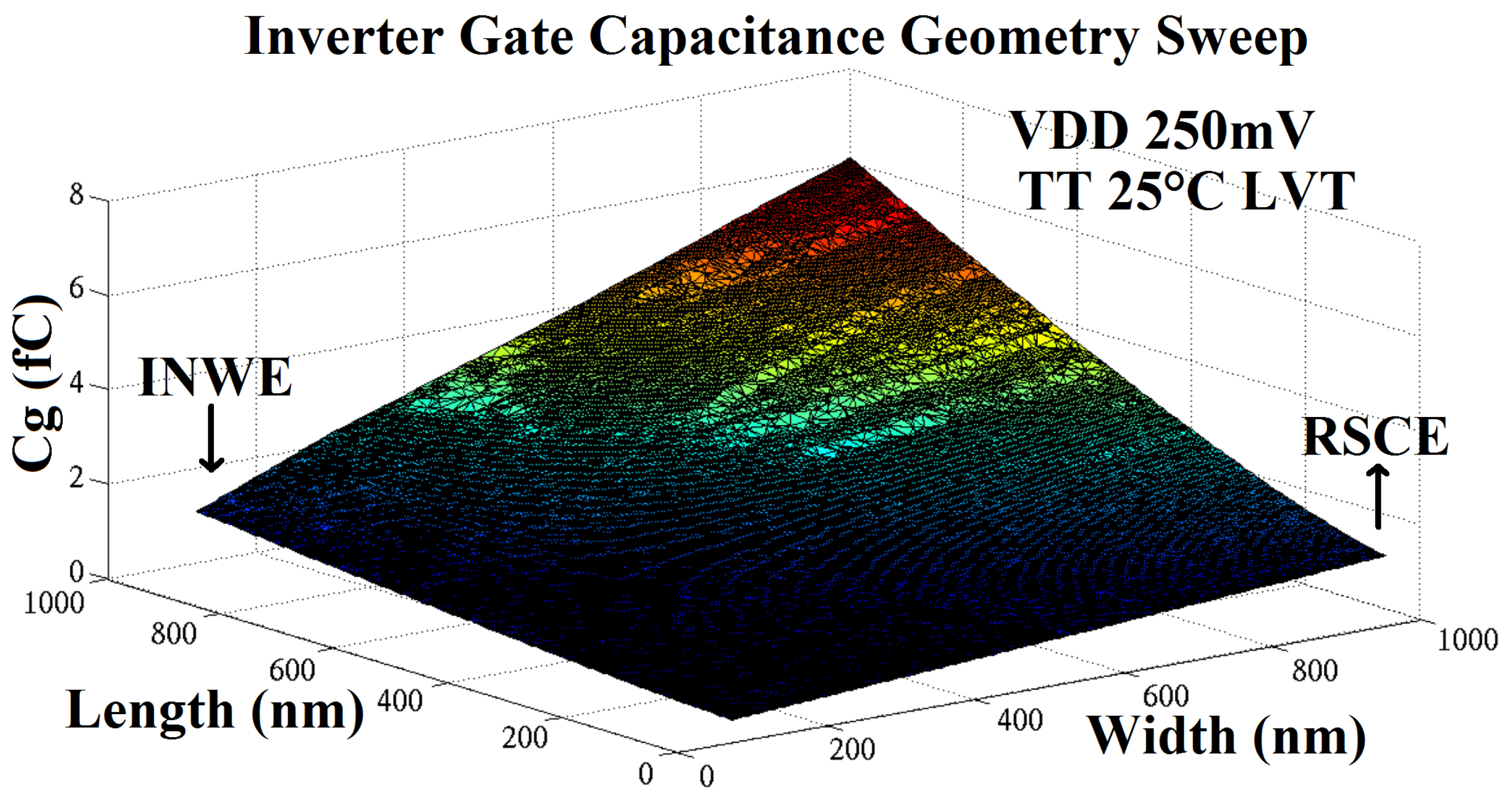
Both INWE and RSCE are theorised to reduce gate capacitance. The addition of the INWE fringing field depletes the device deeper for a fixed gate voltage, reducing the depletion capacitance and therefore gate capacitance per square micron. The lower dopant density of RSCE has the same effect. To determine the impact on the chosen technology node, a test bench was created to simulate the gate capacitance. Due to the complimentary switching of the source and drain during a switching event, the effective gate capacitance is not the same as the static gate capacitance and is dependent on the switching speed. A 5-stage FO4 inverter chain was created with two input forming stages and two output loading stages connected to the device under test (DUT). A duplicate of the DUT was then branched and loaded with a dummy capacitance. A SPICE optimizer was then set to iterate the test bench, altering the dummy capacitance until the rising and falling transitions of both DUTs matched, indicating that the effective gate capacitance had been determined. Tight convergence constraints resulted in a failure of 5% of the test cases. The successful data were then processed using Delauny triangulation to generate a 2D mesh and a TriSurf plot generated. Figure 3 shows such a plot for an LVT inverter at the typical corner. The gate capacitance decreased at a faster rate as the width was reduced, indicating the effect of INWE, and decreased at a slower rate as the length was reduced, indicating the effect of RSCE. Due to the lower dopant densities in the channel, these effects were observed to be greater in LVT. A reduction in gate capacitance and therefore dynamic energy consumption can be achieved by geometric optimisation mindful of these effects.
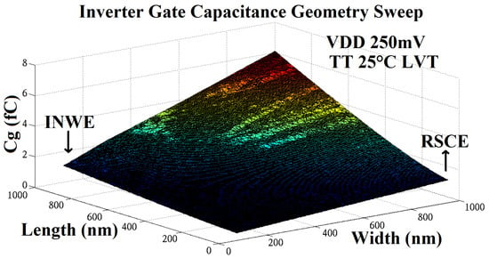
Figure 3.
Simulated gate capacitance geometric sweep.
4.3. Propagation Delay
A 5-stage FO4 (Fan-Out of 4) inverter chain to simulate the average propagation delay (a function of both current and capacitance) was created and geometrically swept in the same fashion. Measurements consisted of rising/falling triggers taken on the input and output at the 50% VDD boundary. Figure 4 shows the sweep for the LVT inverter at the typical corner. RSCE pushed the average propagation delay lower as device length was increased from minimum, towards an optimum length, before beginning to rise once again. For the LVT TT corner, the optimum length was 150 nm, up from the minimum length of 60 nm. INWE pushed the average propagation delay lower as the device width tended towards a minimum. Once again, these effects displayed a greater impact on LVT devices. The result of this was better delay optimisation for LVT devices at the cost of larger LVT footprints (increase in device length equates to an increase in standard cell width).
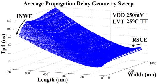
Figure 4.
Simulated average propagation delay geometric sweep.
4.4. Minimum Operating Voltage
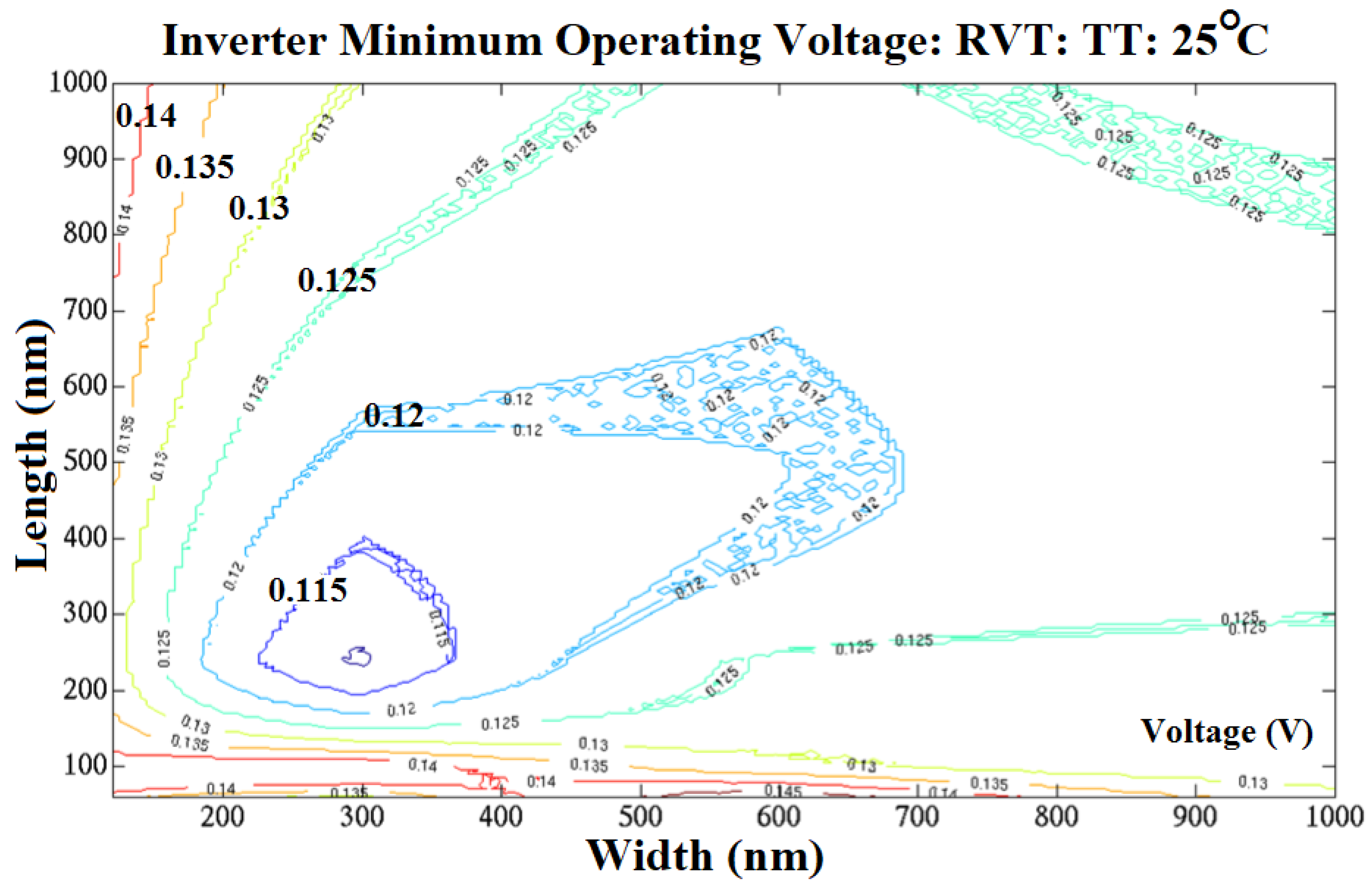
Under aggressive voltage scaling, MOS devices begin to exhibit ohmic behavior, with the voltage dropped across them accounting for a larger proportion of the rail to drain voltage, degrading the voltage swing and therefore noise margins. By definition, CMOS logic may only be deemed functional with positive noise margins. A test bench was created to test the impact of device geometry on this form of robustness. The test bench generated the voltage transfer characteristic of a geometrically balanced inverter by sweeping the input voltage. The input high and input low voltage thresholds were determined at the points where the first order derivatives of the transfer characteristic equal −1, common practice within the field. The output low and output high voltages were determined at the corresponding input voltages. The practical minimum operating voltage was then determined to be the point at which the high or low noise margin was reduced to 10% of the supply voltage (also common practice). The test bench was swept geometrically across the same 5 nm manufacturing grid as the other test benches. Figure 5 shows the RVT inverter results for the typical corner. A local minimum of 109 mV was observed at a length/width of 240 nm/300 nm. For LVT, the focal point was much higher in both dimensions and greater in magnitude at 133 mV. This is likely due to the greater current contention of the complementary off device, a result of the lower Ion/Ioff ratio. The high gradient from the minimum dimensions to the focal point (apparent in both VT’s) demonstrates that a large improvement in robustness may be achieved by only a slight upsizing in geometry.
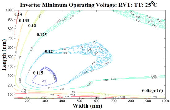
Figure 5.
Simulated minimum operating voltage geometric sweep.
4.5. Standard Cells
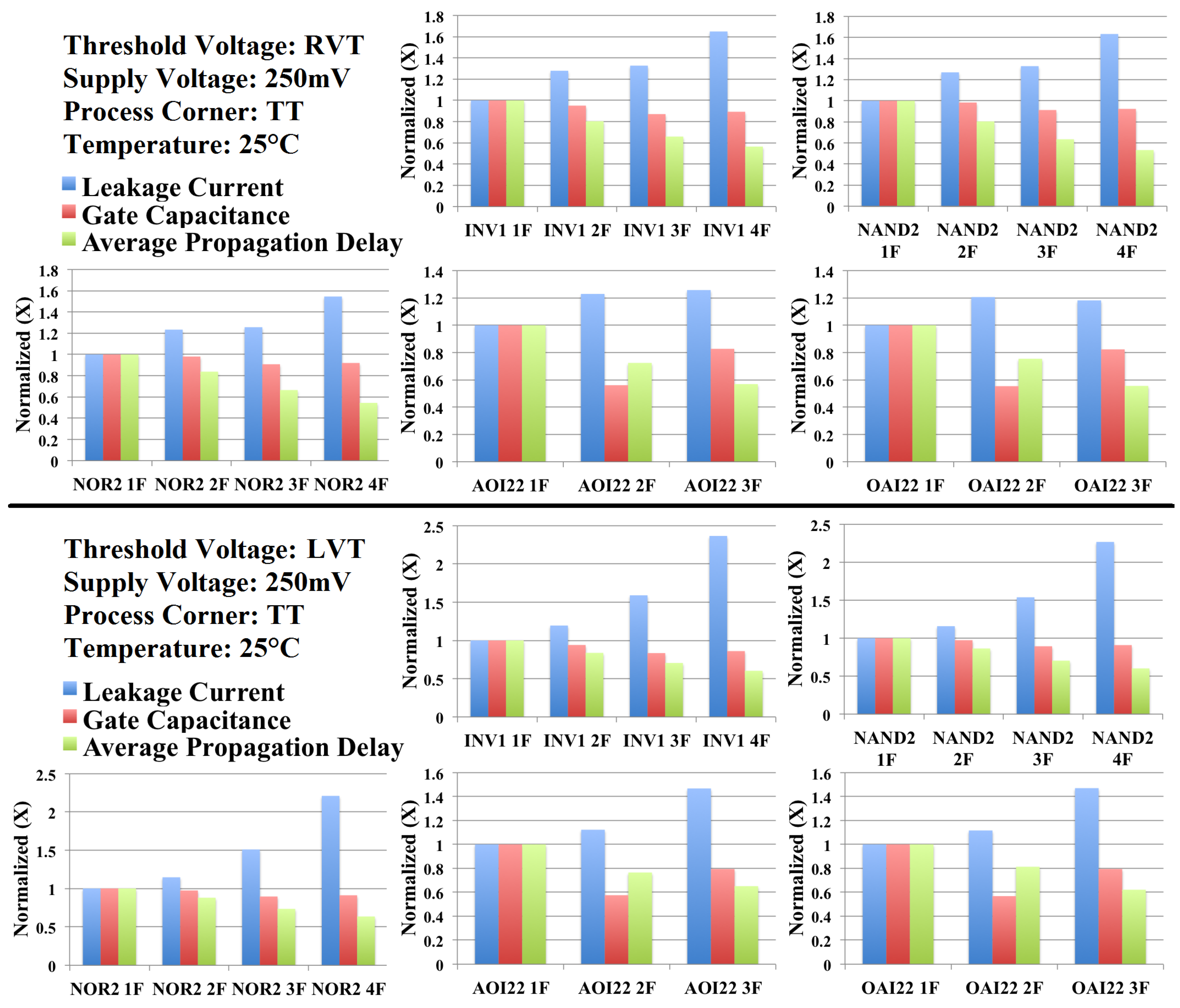
Combinational and sequential cells were laid out, parasitically extracted and characterised in a commercial EDA workflow. Cells included INVX1, NAND2, NOR2, AOI22, OAI22, Pre-Integrated Clock Gate and D-Type Flip-Flop with Asynchronous Reset. These cells were supported with INV/BUFFER cells with drive strengths from X2 to X8 and the usual ancillary cells (FillCaps, Ties, etc.). Equal P/N sizing was used to create the maximum number of finger permutations in the pull up/down networks in keeping with the original study [9], although the technique could also be used to create balanced cells. The technique itself did not increase the cell footprint; however, simultaneous RSCE optimization increased some cell widths as highlighted in the previous sections. For the typical corner, the RSCE optimal length was 150 nm for LVT devices regardless of finger width. For RVT, these were 90 nm for 1–2 fingers and 100 nm for 3–4 fingers. Figure 6 shows performance/leakage characteristics from a sample of the combinational cells. The trend of leakage increase and gate capacitance/propagation delay decrease is observed across cell types, with a minor deviation in the AOI22/OAI22 3 finger variant where additional diffusion struts were required to make the cell viable. The reduction in gate capacitance was primarily a result of reduction in gate area from the technique supplemented by reductions in depletion capacitance as outlined in earlier sections.
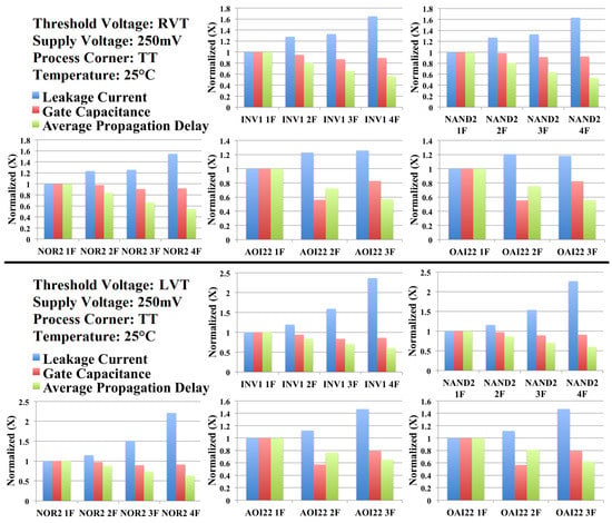
Figure 6.
Simulated cell characterisations.
5. Synthesis Methodology
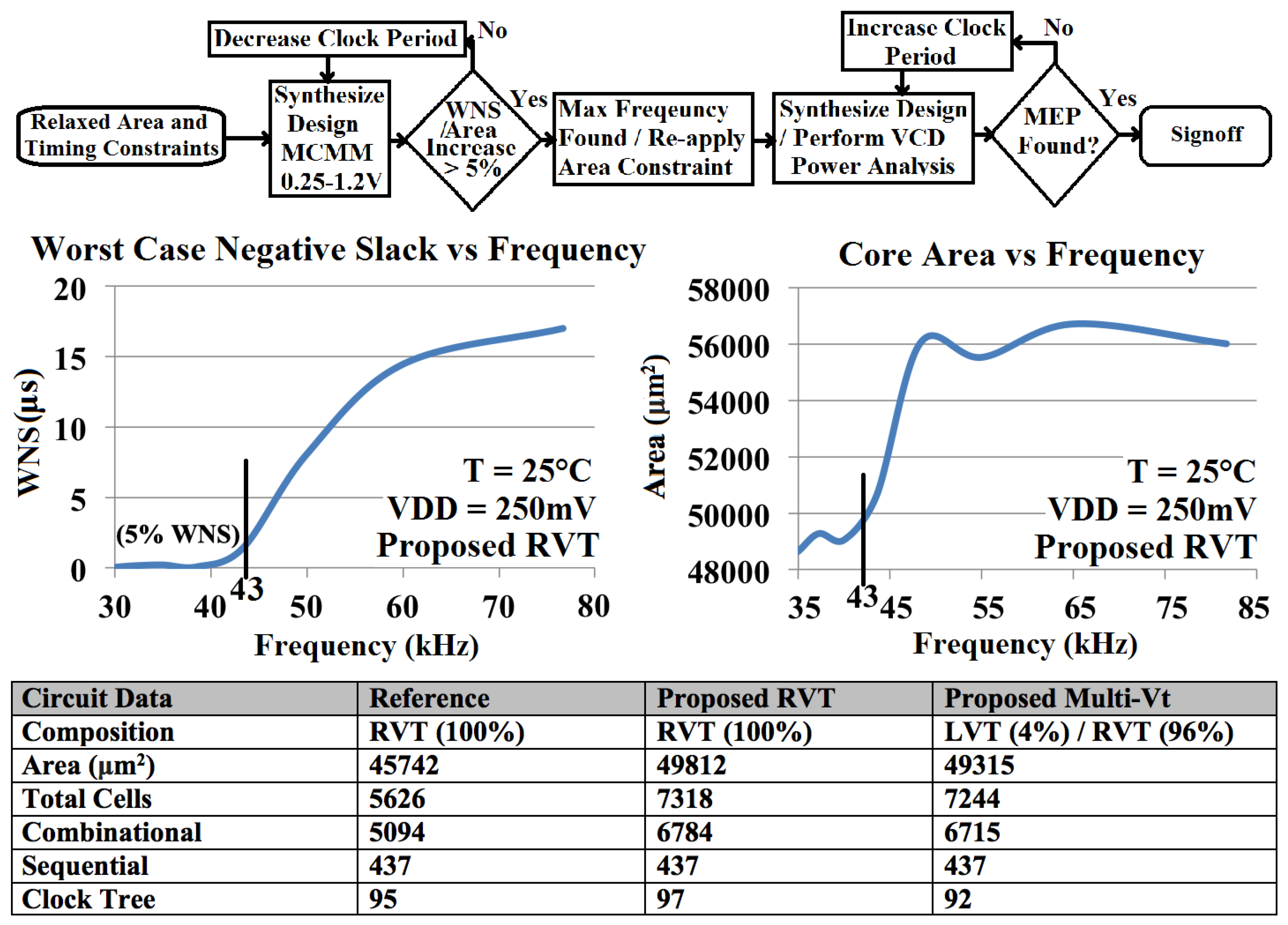
A commercial EDA synthesis toolchain was used to synthesize 32-bit datapath 128-bit AES cores with tightly coupled logical built-in self test (LBIST). Three cores were sythesised; proposed RVT only, proposed Multi-Vt and one from a state-of-the-art subthreshold library. All cores were synthesized from identical RTL, and all libraries contained the same logic gates. Two stages of synthesis were performed: maximum frequency and minimum energy point (MEP).
To determine the maximum frequency, an initial relaxed timing constraint was provided along with a variable area constraint and fixed area utilisation ratio of 80%. This allowed the design to expand as required. Design synthesis, placement, clock-tree synthesis and routing were then conducted. The final design was then parasitically extracted and static timing analysis performed using generated standard delay format (SDF) data. This process was then iterated over stricter timing constraints until a 5% worst case negative slack (WNS) was achieved. This helped to eliminate non-deterministic results from the workflow. Figure 7 shows the characteristic WNS and area explosion as the tools attempt to meet the timing constraint through buffer insertion.
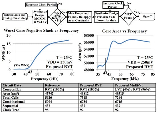
Figure 7.
Synthesis methodology (data simulated after parasitic extraction).
Maximum frequencies of 23.5 kHz, 42.8 kHz and 414.9 kHz were determined for the reference, proposed RVT and proposed Multi-Vt libraries, respectively. These account for 82%/17.7× improvements for proposed RVT and proposed Multi-Vt libraries, respectively. Even with the inclusion of leakage recovery, the synthesis tool implemented the Mutli-Vt core with 96% LVT cells and 4% RVT cells.
To determine the minimum energy point, the maximum frequency was provided as the initial timing constraint along with a fixed area constraint as measured at the maximum frequency and a variable area utilisation ratio. The same synthesis stages were performed as above but the parasitically extracted design, complete with SDF timing data, was then simulated with a test vector using a commercial EDA simulation tool over 20 BIST cycles. This produced a value change dump (VCD) containing net toggle data. This was then passed back into the static timing analysis tool to generate accurate power and dynamic/leakage energy data. The whole synthesis was then iterated over relaxing timing constraints until the full total energy curve was established. The signoff frequency chosen for each core was the frequency at the minimum energy point. These were 16.79 kHz/25.22 kHz/51.87 kHz for the reference, proposed RVT and proposed Multi-VT, respectively, giving energy-per-cycle values of 3.27 pJ/3.81 pJ/3.28 pJ. Contrary to the intuition of the underlying physics, this suggested that the proposed technique might produce less efficient designs. Figure 7 shows the signoff design metrics. The Multi-Vt core consisted of 4% LVT and 96% RVT cells, a complete reversal of the maximum frequency synthesis VT breakdown. The cell counts for the proposed RVT and proposed Multi-Vt libraries were 30%/28.6% greater, respectively. However, the total area increase was only 8.9%/7.8%. Investigation revealed the cell count increase to be logical decomposition by the synthesis tool as a result of the richer variety of cells provided by the proposed technique. Cell width increase from RSCE optimization accounted for the majority of the area increase.
6. Measured Results
6.1. Nominal Operation
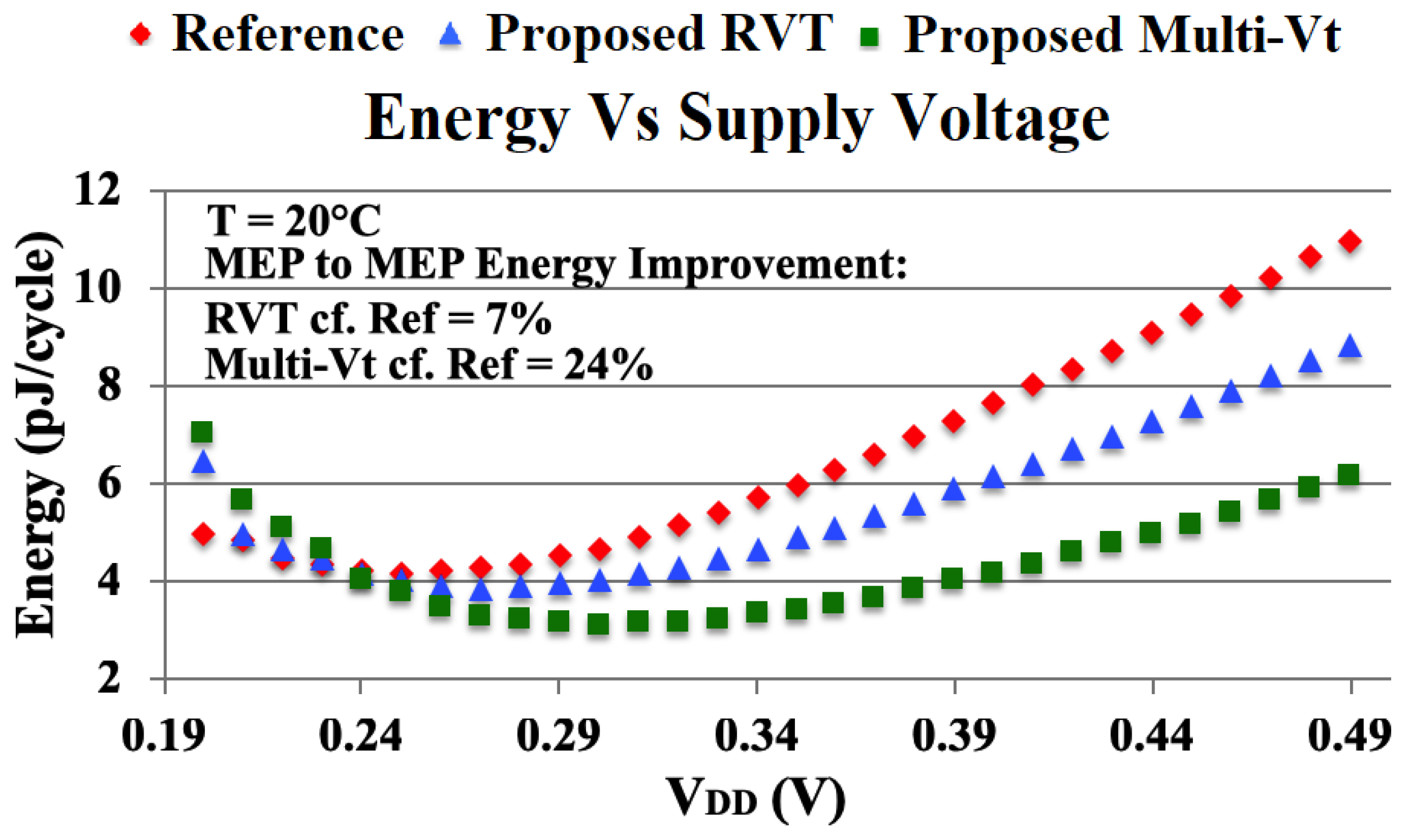
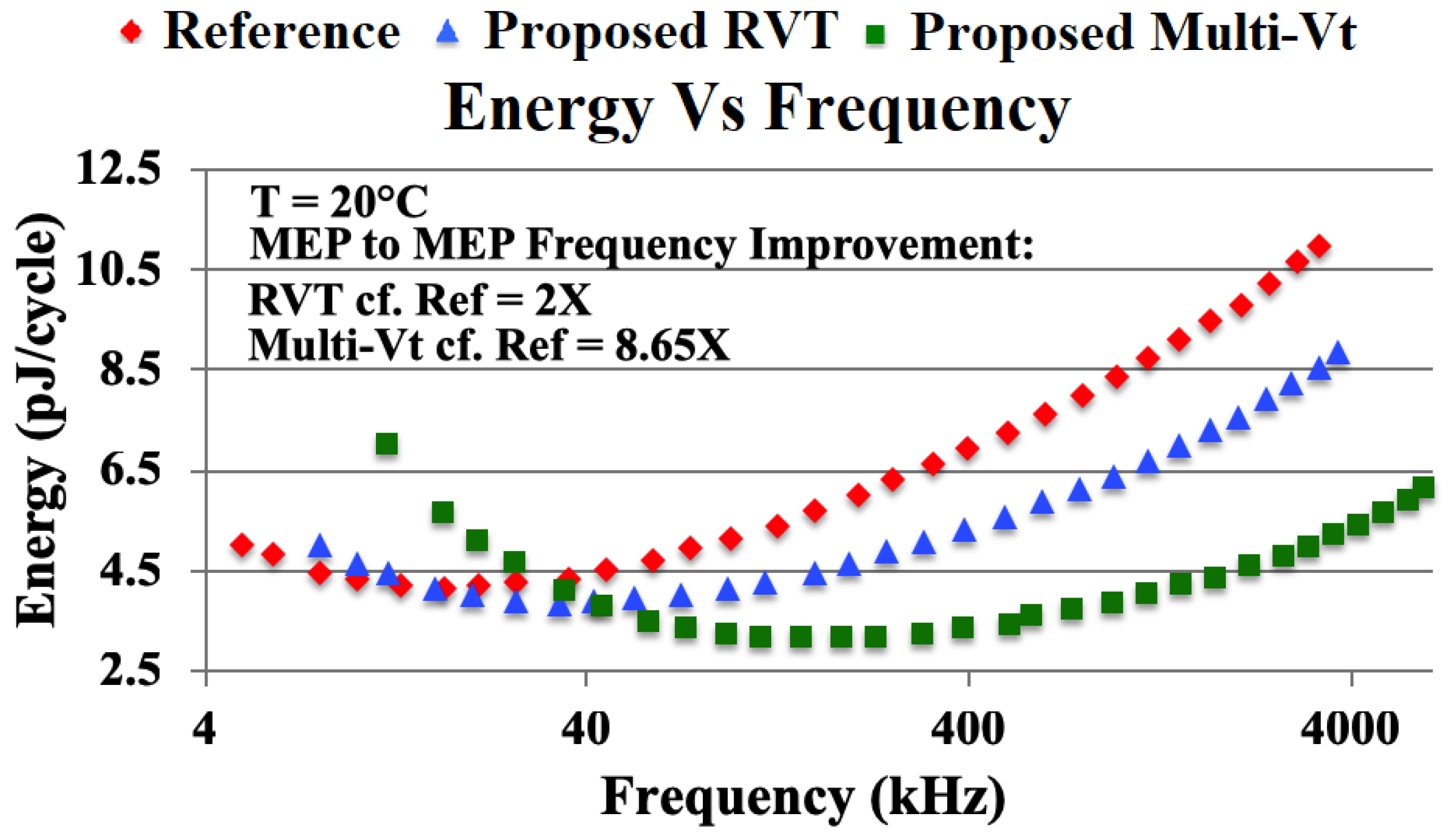
Figure 8 and Figure 9 show the relevant metrics under nominal operation—MEP to MEP at nominal temperature (20 °C), the total energy-per-cycle of the cores measured 4.12 pJ/3.84 pJ/ 3.11 pJ for the reference, proposed RVT and proposed Multi-Vt cores, respectively. This represents energy improvements of 7%/24% compared to the reference core and suggests that the BSIM4.5 models used to simulate the signoff designs underestimated the energy requirements of the reference design and overestimated the energy requirements of the proposed designs. The frequencies of the cores measured 17 kHz/34 kHz/147 kHz for the reference, proposed RVT and proposed Multi-Vt cores, respectively. This represents frequency improvements of 2×/8.65× compared to the reference core. Whilst the signoff simulations appear to have accurately predicted the performance of the reference design, they largely underestimated the performance increase of the proposed technique.
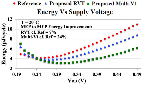
Figure 8.
Measured nominal AES core results—energy over voltage scaling.
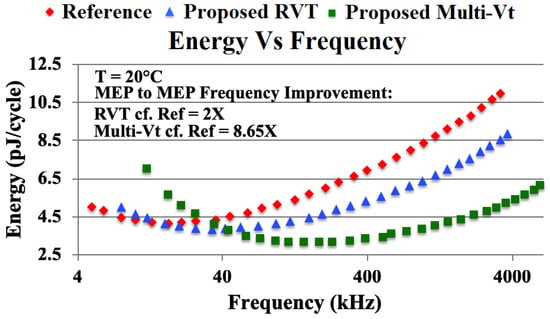
Figure 9.
Measured nominal AES core results—MEP frequency.
The combined effect of an increase in leakage current and decrease in dynamic energy consumption consistently pushed the MEP lower in energy and to a higher supply voltage and frequency across the measured temperature range (0 °C–85 °C), as compared to the reference library. This suggests further energy gains may be available at the circuit level by the application of techniques such as power gating or duty cycling to further reduce or eliminate leakage energy. These techniques display higher benefit to the previously cited work [5], where energy gains were already derived from leakage energy reductions. Moreover, higher supply voltage operation results in reduced sensitivity to local and global variation, as well as easing efficient DC-to-DC voltage regulator design [10].
6.2. Temperature Analysis
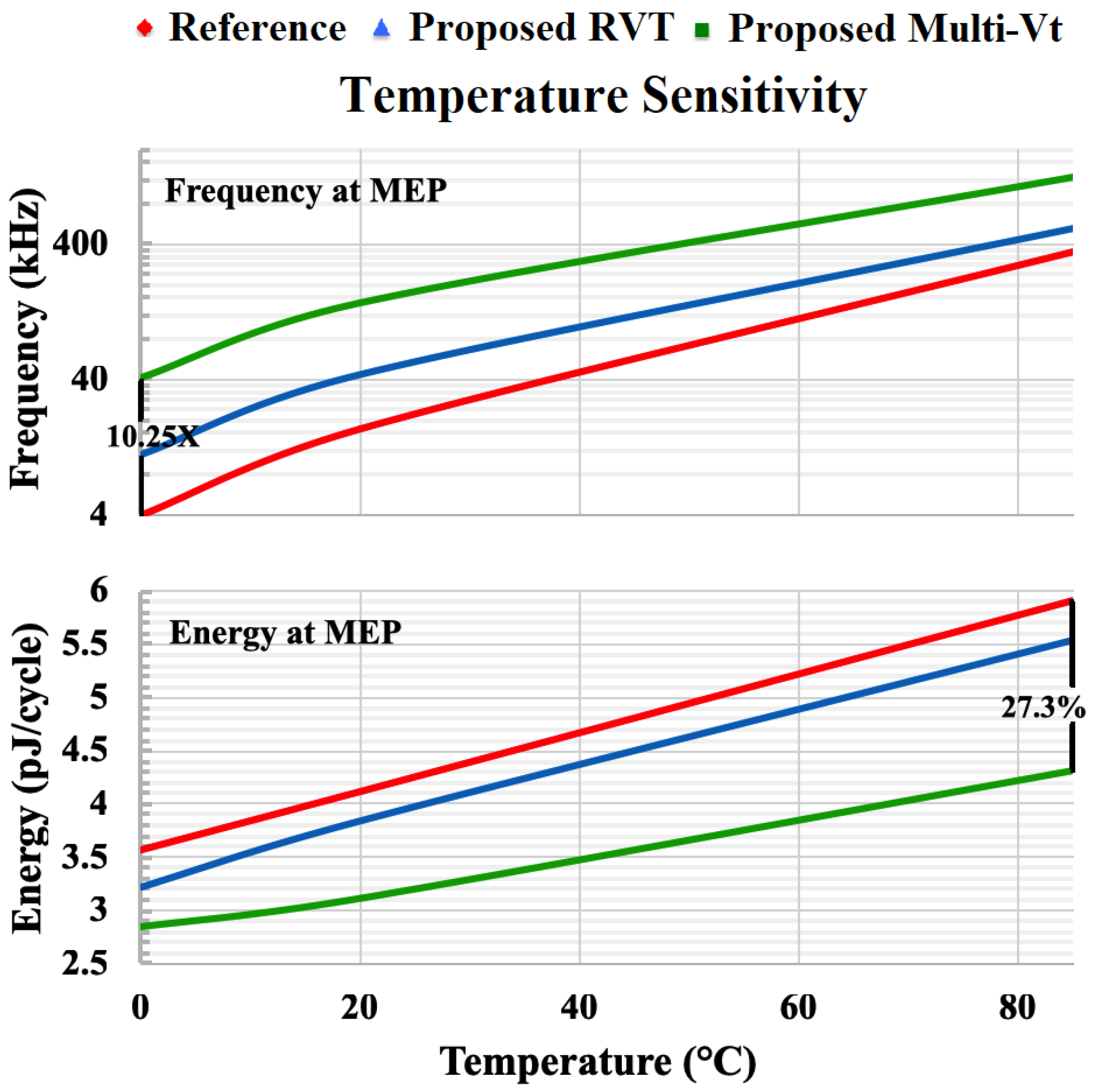
Figure 10 shows frequency and energy under thermal variation. Temperature sweeping revealed maximum comparative gains of 10.25× in frequency (Proposed Multi-Vt compared to Reference at 0 °C) and 27.3% in energy per cycle (Proposed Multi-Vt compared to Reference at 85 °C). This suggests that the performance compensation to temperature inversion is exhibited even in complex circuitry.
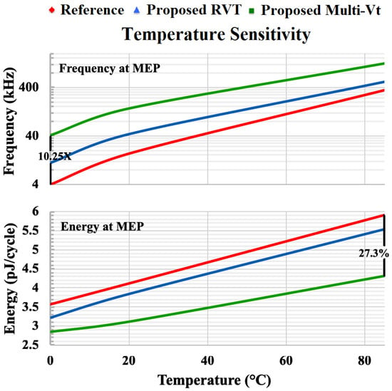
Figure 10.
Measured thermal AES core results.
6.3. Interdie Variation
Figure 11 shows interdie variation. A random 10 chip sample revealed maximum frequency deviations from mean of 7.7%/5.8%/9.1% at MEP for the reference, proposed RVT and proposed Multi-Vt, respectively. The higher deviation for the Multi-Vt core is likely relative tracking variation between the LVT/RVT implant stages. No core from the 30 core sample malfunctioned at its MEP.

Figure 11.
Measured interdie variation of AES cores.
6.4. Comparison to Alternate Geometric Sizing Strategies
A comparison to alternate geometric sizing strategies may be seen in Table 1.

Table 1.
Prior art comparison.
7. Discussion
7.1. Performance
The study indicated correlation between RSCE optimal sizing and device width. Thus, any INWE aware sizing strategy must incorporate RSCE, especially at low device width where deviation from SCE length sizing is greatest. Whilst RSCE aware sizing increases gate area, simulation showed it also reduces depletion capacitance. Its effect on dynamic energy consumption is therefore technology node dependent. The addition of STI spacers for INWE aware sizing reduces both gate area and depletion capacitance but increases leakage current. The benefits of the proposed library are therefore maximised in complex circuitry with a large range of path delays, where leakage recovery can make the greatest energy savings by switching fast cells out for a lower finger variant with an improved performance-to-leakage metric.
7.2. Variation
The distance of mechanical stress interaction (length of oxide definition) is determined to be 2 μm in deep submicron bulk planar nodes. The introduction of STI spacers therefore increases cell variation as a result. Variation analysis during the study showed that the 4 finger design proved least variable in LVT for the chosen technology node. The impact of stress variation is therefore minimal. Whilst fingering should theoretically increase variation from RDF due to its proportionality to the inverse of the square root of the quadrature, the 4 finger LVT cell shows the averaging effect of multiple variable devices can produce a superior cell in the chosen node. The impact of fingering on line edge roughness variation could not be determined from the study due to the composite nature of the cells under test.
7.3. Future Work
Given that the primary physical effect leveraged in the proposed technique is the fringing field of the gate, body-biasing may also provide a further boost in energy efficiency and performance. Application of the technique to FD-SOI is feasible but will depend on the geometric isolation characteristics of the specific technology node. As the geometry of finFET transistors is already quantized, the proposed technique offers no further gains.
8. Conclusions
This work presented 128-bit AES cores synthesized from subthreshold standard cell libraries created by geometric STI spacer patterning in a 65 nm LP bulk planar process. Nominal temperature (20 °C) analysis revealed improvements of up to 8.65×/24% MEP-to-MEP in frequency and energy-per-cycle, respectively, compared to a state-of-the-art subthreshold library. A negative temperature correlation with performance enhancement was demonstrated extending beyond cell level and into more complex designs. MEP-to-MEP performance enhancement and energy-per-cycle reduction were demonstrated over a temperature range of 0 °C to 85 °C.
Author Contributions
Conceptualization, J.M. (Jordan Morris) and J.M. (James Myers); methodology, J.M. (Jordan Morris), P.P. and J.M. (James Myers); software, J.M. (Jordan Morris); validation, J.M. (Jordan Morris) and P.P.; formal analysis, J.M. (Jordan Morris) and P.P.; investigation, J.M. (Jordan Morris); resources, J.M. (James Myers); data curation, J.M. (Jordan Morris); writing—original draft preparation, J.M. (Jordan Morris); writing—review and editing, J.M. (Jordan Morris), P.P., J.M. (James Myers) and A.Y.; visualization, J.M. (Jordan Morris); supervision, P.P., J.M. (James Myers) and A.Y.; project administration, J.M. (James Myers) and A.Y.; funding acquisition, A.Y. All authors have read and agreed to the published version of the manuscript.
Funding
This research was jointly funded by the Engineering and Physical Sciences Research Council (EPSRC) and Arm Ltd.
Institutional Review Board Statement
Not applicable.
Informed Consent Statement
Not applicable.
Data Availability Statement
The subthreshold library presented is available from the author. The author requests that any resultant work cites this paper as the appropriate reference for the library.
Acknowledgments
The authors would like to thank Graham Knight for his rapid implementation and integration support.
Conflicts of Interest
The authors declare no conflict of interest.
Abbreviations
The following abbreviations are used in this manuscript:
| AES | Advanced Encryption Standard |
| BIST | Built-In Self Test |
| DIBL | Drain Induced Barrier Lowering |
| DUT | Device Under Test |
| DVFS | Dynamic Voltage and Frequency Scaling |
| EDA | Electronic Design Automation |
| FinFET | Fin Field-Effect Transistor |
| FF | A process corner where both PMOS and NMOS are considered fast |
| INWE | Inverse Narrow Width Effect |
| IoT | Internet of Things |
| LBIST | Logical Built-In Self Test |
| LVT | Low Threshold Voltage |
| MEP | Minimum Energy Point |
| RDF | Random Dopant Fluctuation |
| RSCE | Reverse Short Channel Effect |
| RTL | Register Transfer Level |
| RVT | Regular Threshold Voltage |
| SCE | Short Channel Effect |
| SDF | Standard Delay Format |
| SoC | System on Chip |
| SS | A process corner where both PMOS and NMOS are considered slow |
| STI | Shallow Trench Isolation |
| TT | A process corner where both PMOS and NMOS are considered typical |
| UWDVS | Ultra-Wide Dynamic Voltage Scaling |
| VCD | Value Change Dump |
| WNS | Worst-Case Negative Slack |
References
- Ghani, T. Scaling Challenges and Device Design Requirements for High Performance Sub-50 nm Gate Length Planar CMOS Transistors. In Proceedings of the 2000 Symposium on VLSI Technology. Digest of Technical Papers (Cat. No.00CH37104), Honolulu, HI, USA, 13–15 June 2000; pp. 31–44. [Google Scholar]
- Kumar, R. Reversed Temperature-Dependent Propagation Delay Characteristics in Nanometer CMOS Circuits. IEEE Trans. Circuits Syst. II Express Briefs 2006, 53, 1078–1082. [Google Scholar] [CrossRef]
- Why Ambiq. Available online: ambiq.com/why-ambiq/ (accessed on 12 May 2022).
- Loyez, C.; Carpentier, K.; Sourikopoulos, I.; Danneville, F. Subthreshold neuromorphic devices for Spiking Neural Networks applied to embedded A.I. In Proceedings of the 2021 19th IEEE International New Circuits and Systems Conference (NEWCAS), Toulon, France, 13–16 June 2021; pp. 1–4. [Google Scholar]
- Kim, T. Utilizing Reverse Short-Channel Effect for Optimal Subthreshold Circuit Design. IEEE Trans VLSI Syst. 2007, 15, 821–829. [Google Scholar] [CrossRef]
- Shigyo, N.; Hiraoka, T. A Review of Narrow-Channel Effects for STI MOSFET’s: A Difference Between Surface- and Buried-Channel Cases. Solid State Electron. 1999, 43, 2061–2066. [Google Scholar] [CrossRef]
- Liao, R. Digital circuit design for robust ultra-low-power cell library using optimum fingers. In Proceedings of the 2012 IEEE 55th International Midwest Symposium on Circuits and Systems (MWSCAS), Boise, ID, USA, 5–8 August 2012; pp. 446–449. [Google Scholar] [CrossRef]
- Pons, M. Ultra low-power standard cell design using planar bulk CMOS in subthreshold operation. In Proceedings of the 2013 23rd International Workshop on Power and Timing Modeling, Optimization and Simulation (PATMOS), Karlsruhe, Germany, 9–11 September 2013; pp. 9–15. [Google Scholar] [CrossRef]
- Morris, J. Unconventional Layout Techniques for a High Performance, Low Variability Subthreshold Standard Cell Library. In Proceedings of the 2017 IEEE Computer Society Annual Symposium on VLSI (ISVLSI), Bochum, Germany, 3–5 July 2017; pp. 19–24. [Google Scholar] [CrossRef]
- Myers, J. A Subthreshold ARM Cortex-M0+ Subsystem in 65 nm CMOS for WSN Applications with 14 Power Domains, 10T SRAM, and Integrated Voltage Regulator. IEEE J. Solid-State Circuits 2016, 51, 31–44. [Google Scholar]
- Calhoun, B.H. Characterizing and modeling minimum energy operation for subthreshold circuits. In Proceedings of the Proceedings of the 2004 International Symposium on Low Power Electronics and Design, Newport Beach, CA, USA, 9–11 August 2004; pp. 90–95. [Google Scholar]
- Kwong, J. Variation-Driven Device Sizing for Minimum Energy Sub-threshold Circuits. In Proceedings of the ISLPED, Tegernsee Bavaria, Germany, 4–6 October 2006; pp. 8–13. [Google Scholar]
- Zhou, J. A 40 nm Dual-Width Standard Cell Library for Near/Sub-Threshold Operation. IEEE Trans. Circuits Syst. I Regul. Pap. 2012, 59, 2569–2577. [Google Scholar] [CrossRef]
Publisher’s Note: MDPI stays neutral with regard to jurisdictional claims in published maps and institutional affiliations. |
© 2022 by the authors. Licensee MDPI, Basel, Switzerland. This article is an open access article distributed under the terms and conditions of the Creative Commons Attribution (CC BY) license (https://creativecommons.org/licenses/by/4.0/).

