Abstract
This work presents various essential features and design aspects of a single-inductor, common-output, and multi-string White Light Emitting Diode (WLED) driver for low-power portable devices. High efficiency is one of the main features of such a device. Here, the efficiency improvement is achieved by selecting the proper arrangement of WLEDs and a proper sensing-circuit technique to determine the minimum, real-time, needed output voltage. This minimum voltage necessary to activate all WLEDs depends on the number of strings and the forward voltage drops among the WLEDs. Advanced CMOS technology is advantageous in mixed-signal environments such as WLED drivers. However, this process suffers from low on-resistance, which degrades the accuracy of the current sinks. To accommodate the above features and mitigate the low node process issue, a boost-converter that is single output with a load of a three-string arrangement, with 6 WLEDs each, is presented. The designed driver has an input voltage range of 3.2–4.2V. The proposed solution is realized with ultra-low power consumption circuits and verified using ADS tools utilizing 40 nm 1P9M TSMC CMOS technology. An inter-string current accuracy of 0.2% and peak efficiency of 91% are achieved with an output voltage up to 25 V. The integrated WLED driver circuitry enables a high switching frequency of 1MHz and reduces the passive elements’ size in the power stage.
1. Introduction
WLED drivers are ubiquitous when it comes to modern smart portable devices. They provide a backlight plus dimming and brightness control. A DC-DC boost converter is very popular in building WLED drivers [1,2]. The available input voltage is usually the battery voltage (3.2 V to 4.2 V), while the needed output voltage is, relatively, much higher. A WLED driver based on a boost converter can be thought of as a boost converter with one or more WLED strings functioning as its load. Figure 1 illustrates a multi-string boost-based WLED driver with a common output. Each string may contain one or more WLEDs powered by a current source to control the degree of illumination intensity. The electrical current that flows through the WLED determines its brightness. The forward voltage drop of a typical WLED varies depending on the type of semiconductor used in its fabrication and the manufacturing process’s tolerances [1].
Figure 1.
The architecture of a single-inductor, common-output, multi-string boost-based WLED driver.
As per [3], the White LED journey started after discovering the blue LED by Shuji Nakamure in Japan. The first white light source was developed by mixing lights from red, green, and blue LEDs together. As this method is deemed to be expensive, the most recent method to produce white light is by adding a phosphorous layer to the blue LED, which modifies the emission spectrum. The blue light excites the phosphorus and allows it to emit yellow light. Combining both yellow and blue lights produces the appearance of white light. Figure 2 shows the relationship between the actual white light spectrum and the human eye’s sensitivity to white light. Unfortunately, unlike red, yellow, and green LEDs, circuit drivers for WLEDs (e.g., InGaN LEDs) are more challenging to develop than conventional LEDs (e.g., GaAs, SiGe). As a result, customized WLED drivers are necessary.
Figure 2.
The relation between the actual white light spectrum and the human eye sensitivity to white light.
When it comes to designing a WLEDs driver, there are different architectures to consider, including boost-based [4,5], buck-based [6,7], and charge pump-based WLED drivers [8], as well as many others [9,10,11]. Boost-based architectures are preferable for smartphone applications, as the available input voltage, i.e., the battery voltage (3.2–4.2 V), is well below the required output voltage (20–40 V). The standard DC-DC boost converter design, along with its controller, is known in the art [12,13,14,15]. The output voltage of WLED consists of the total voltage drop of WLEDs plus the overhead of the current sink.
Setting the proper output voltage in a common-output multi-string WLED is challenging, as the required voltage to satisfy all WLEDs may vary. In addition, each string should have the same current to keep consistent backlighting. Sensing the output voltage from the top of the strings [5] should account for worse possible WLED drops in addition to the overhead voltage () of the current sink. This ensures that all WLEDs are activated. In such a control scheme, the other strings have a higher voltage than needed and, thus, consume power unnecessarily. To improve the efficiency of these, voltage might be sensed across the current sink [16]. Moreover, an amplifier-boosted current sink is proposed in this paper, with a programmable resistor bank being used in this paper to ensure that the same current passes through each string.
Most published WLEDs are realized by discreet components [5,6,9,17]. However, these solutions occupy a larger PCB area and, thus, are not suitable for system-on-chip implementation. Using integrated processes such as the 40 nm is more promising for portable devices; for example, this process is commonly used in smartphones [18]. Moreover, this process results in smaller gate capacitance and, thus, lower gate drive loss at high switching speed (>1 MHz) [19], which allows reducing passive elements’ size in the power stage. Furthermore, the 40 nm process is superior to other higher nodes in mixed-signal implementation, such as the WLED driver. However, this process yields a low that jeopardizes the illumination intensity and current matching accuracy. To accommodate the above features and mitigate the low node process issue, a boost-converter that is common-output with a load of a three-string arrangement, with 6 WLEDs each, is presented. This design features a dedicated amplifier-boosted n-MOS current sink circuitry. The selected current sink circuitry comprises a programmable resistor that allows for segmented driver output current [1]. This results in an enhanced inter-string current accuracy and WLED driver efficiency. The paper illustrates, with a design example, the best practices and circuit techniques to address key aspects of the WLED drivers’ design.
All the investigated features and issues are built into the proposed solution. Their circuit implementations are further discussed in more detail in Section 2. The simulation results of the proposed circuit and their comparison to the prior art are explained in Section 3. Section 4 has the conclusion and summary of the key points.
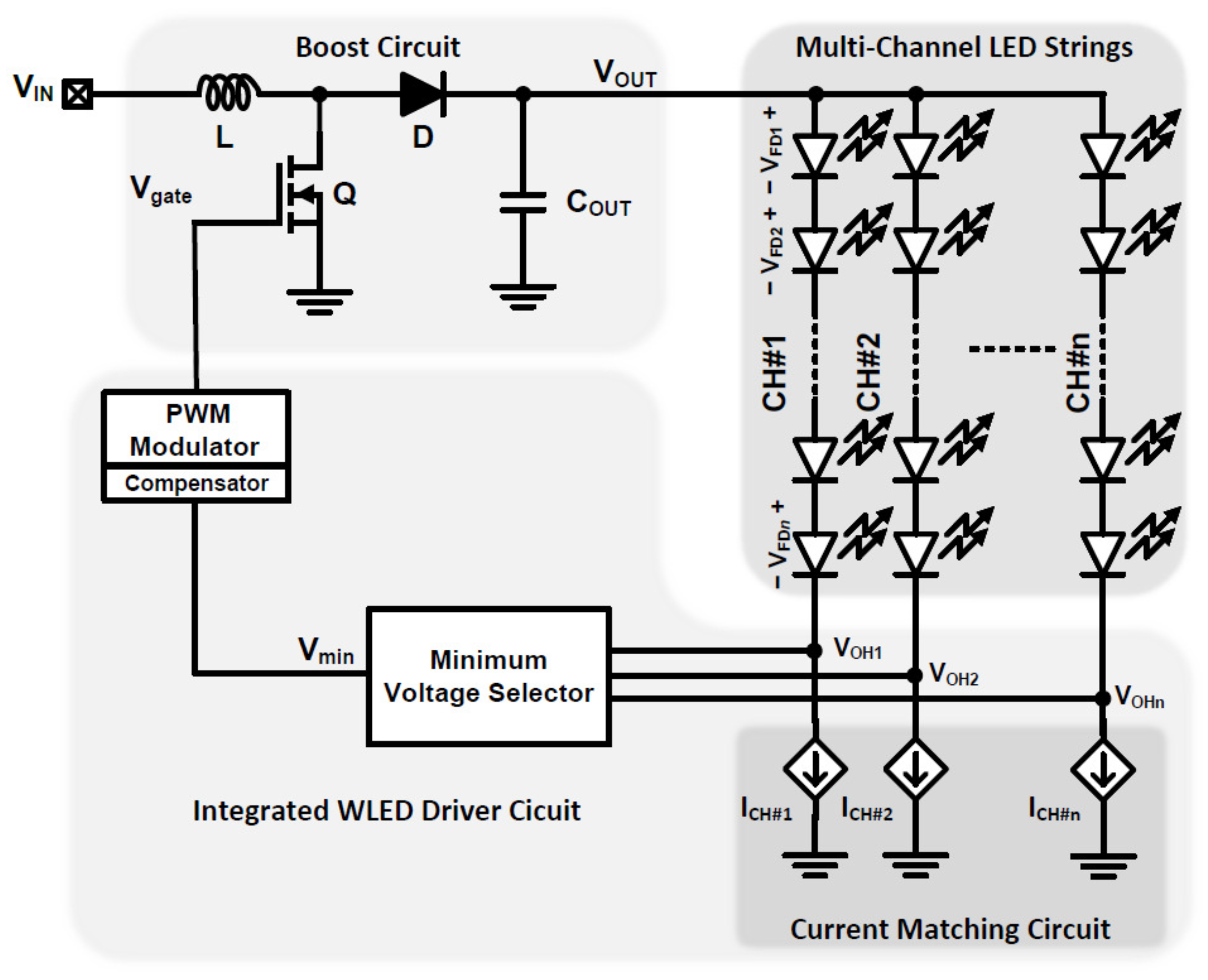
2. Features, Issues and Proposed Circuit Implementation
This section discusses the main design aspects of WLED drivers and the circuits’ implementation.
2.1. Efficiency Optimization
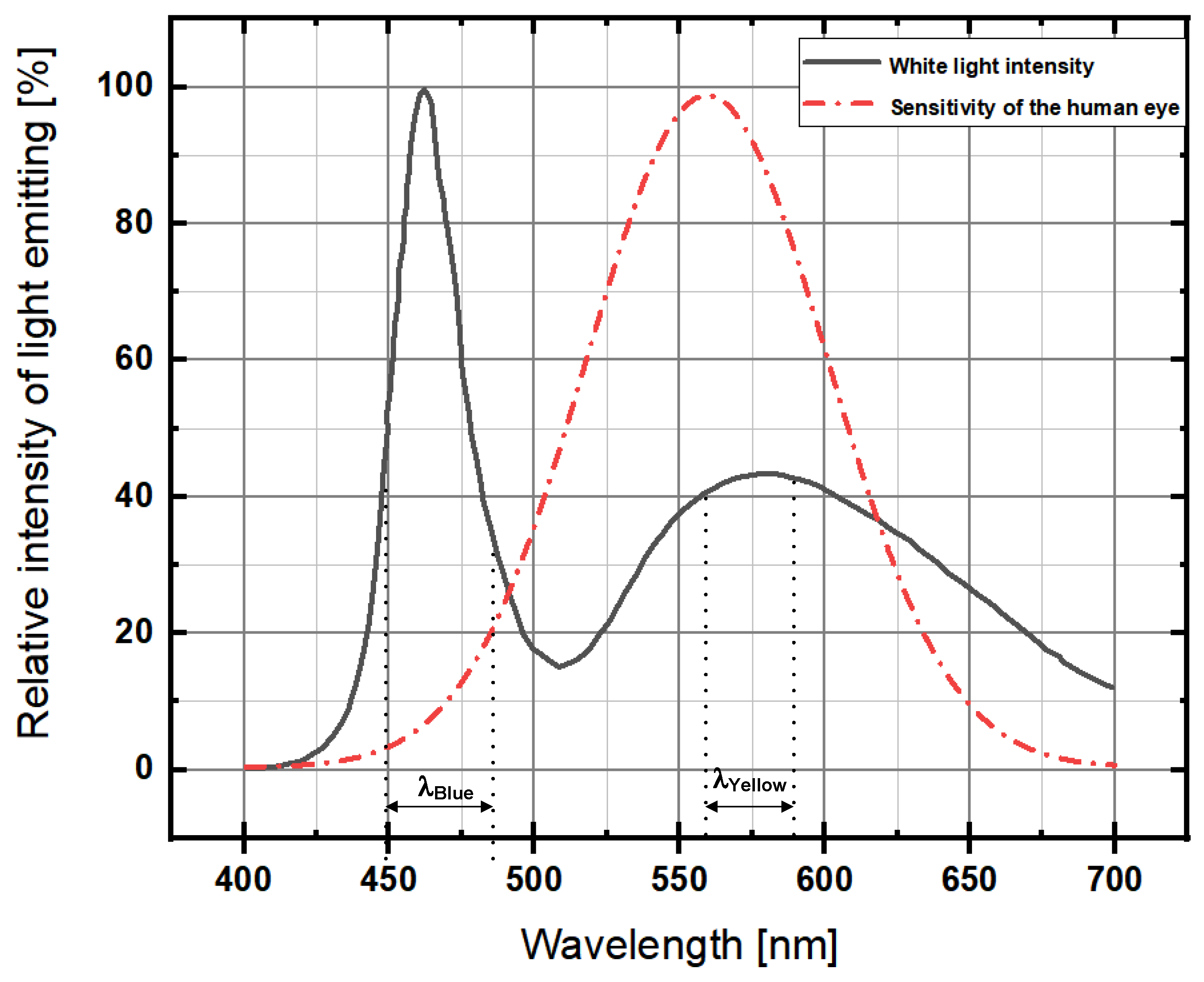
2.1.1. WLED Arrangement
The string arrangement (number of string × number of WLEDs) significantly affects the WLED driver’s efficiency. To accommodate 18 WLEDs, which are enough for the backlighting of an average screen-size smartphone, all possible combinations with varying efficiency values are summarized in Table 1. The equations used to develop the efficiency calculations can be found in [20]. The arrangements listed in Table 1 show that the highest efficiency arrangement is the three strings by six WLEDs per string.
Table 1.
String and Number of WLEDs Arrangements.
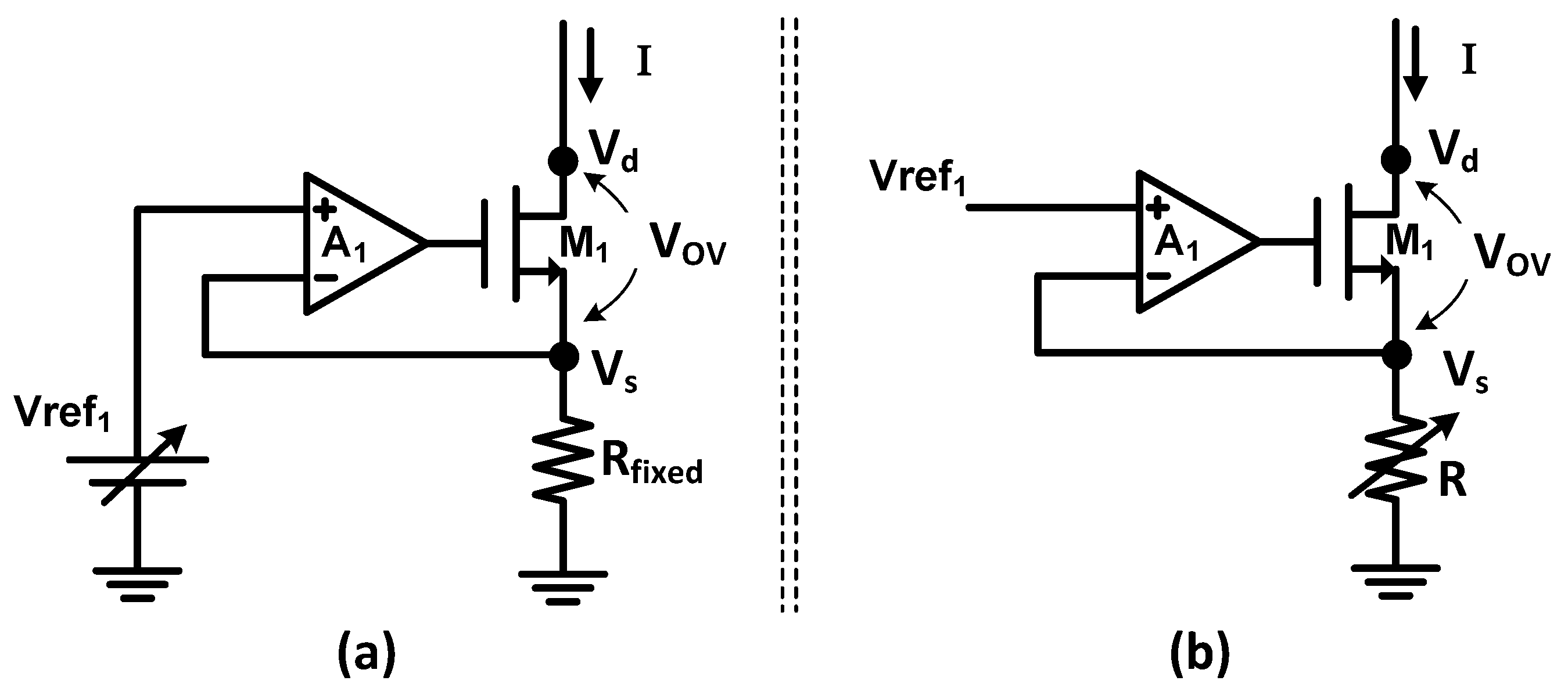
2.1.2. Voltage Feedback Sensing
The minimum, real-time, common-output voltage needed to activate all WLEDs depends on the strings’ highest total forward voltage drops across WLEDs. To reach this voltage, the compensator sets the proper duty cycle correctly by sensing the voltage at an appropriate node, tracking the changes in the . The sensing point can be at the common point of the top of the strings or the top of the current sink. The former option is simpler yet less efficient, as it results in the converter’s output voltage being based on the theoretical pre-set worst-case scenario. The theoretical pre-set worst-case is calculated based on the maximum forward voltage drop of the selected WLED. To illustrate this, in the case of the three-string WLEDs, if the maximum forward voltage drop is 3.5 V [21], then, for a 6-WLED string, the worst-case should be set to 21 V in addition to the overhead voltage of the current sink.
The latter approach sets the required output voltage in real-time, based on the actual total forward voltage drops of the WLEDs plus the overhead voltage of the current sink. To do this, sensing at the top of the current sink is conducted, which forces that point to equal the reference voltage . This indirectly sets the minimum common that ensures that all strings are active. In this approach, once the overhead voltage of the current sink reaches the reference voltage, the corresponding string is active and operational. Since the circuit has three strings, the total voltage drop may vary among the strings. Although reaching the minimum overhead voltage for the worse-case string means that other strings are over-driven, which may cause some inefficiencies. This technique is still more efficient than the former approach. It is noteworthy to mention that sensing the voltage at the top of the current sink is previously discussed in the literature [16]. However, prior-art utilizes external components which are not suitable for high integration CMOS technology. Therefore, an enhanced digital implementation of this technique is developed in this work.
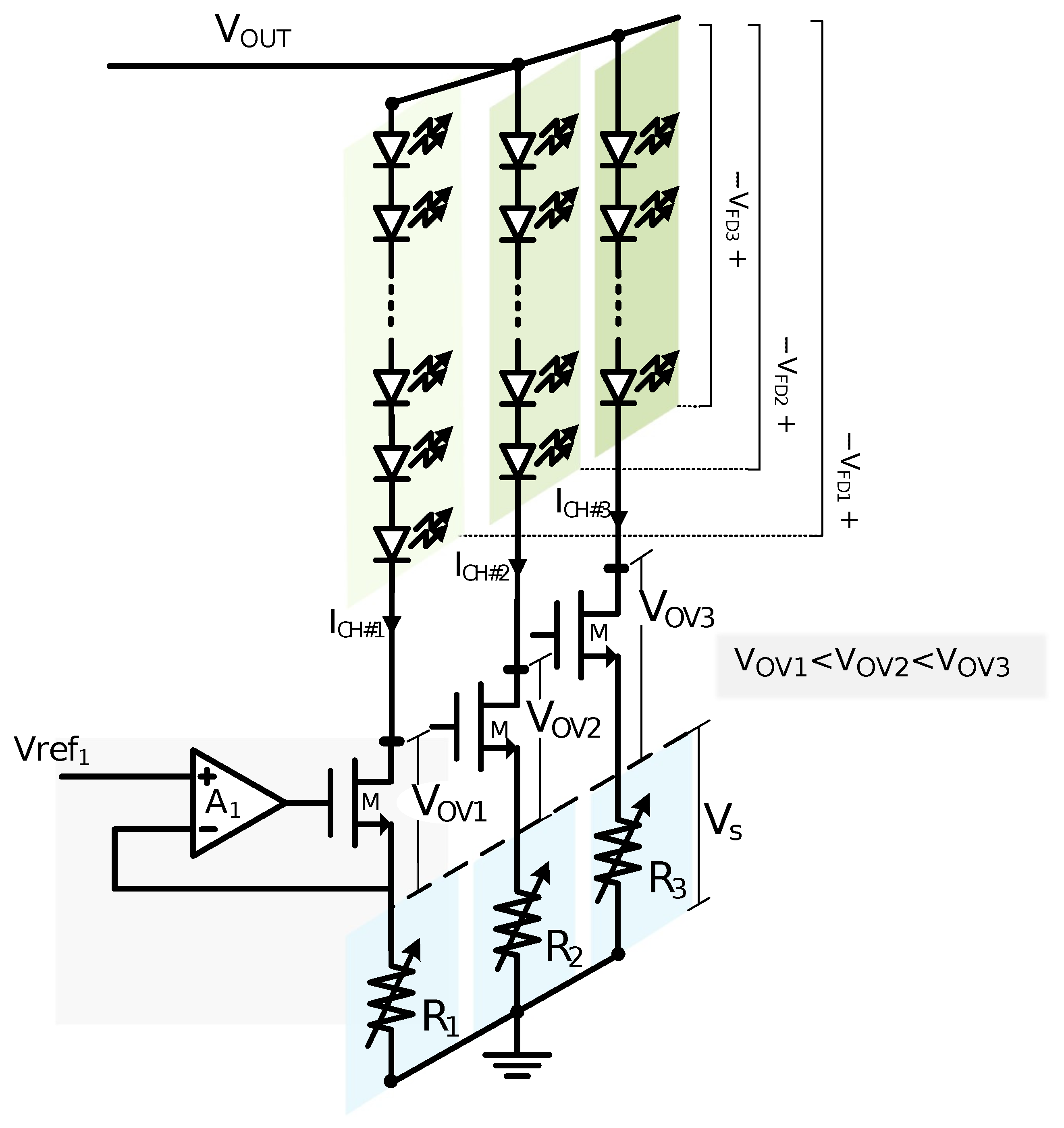
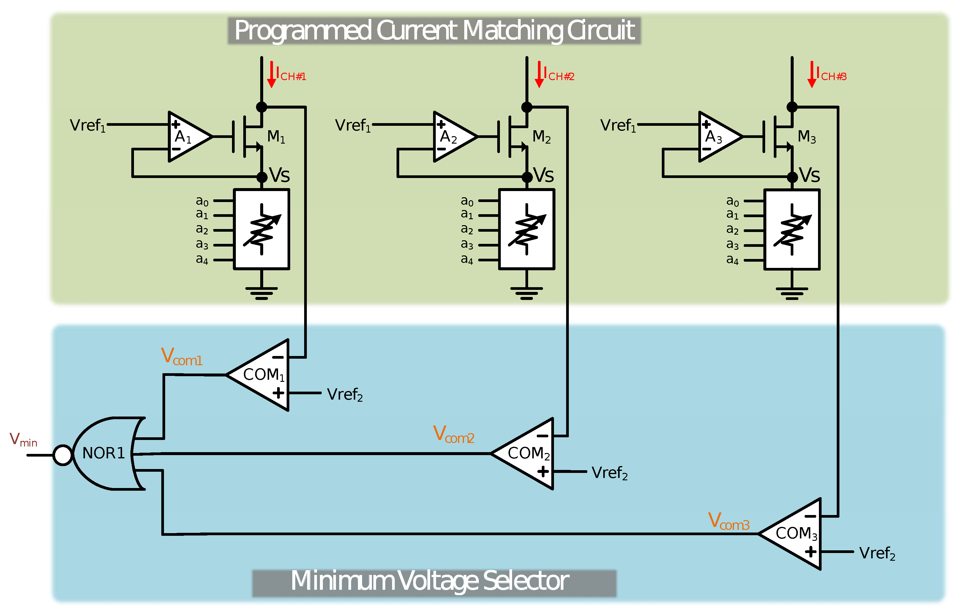
2.2. Current Sink Programmability
To control the backlight brightness, there is a need for a programmable current sink, as shown in Figure 3. This can be achieved either by a configurable resistor bank or a controllable reference voltage [22,23]. The dissipated power in the programable resistor varies linearly with the targeted string current while changing the reference voltage leads to a power dissipation that varies in a quadratic fashion with the targeted string current. The latter solution controls the reference voltage. Then, the voltage across the fixed resistor () is forced to equal the reference voltage with the help of the boosting amplifier (). The targeted string current then equals . On the other hand, the programmable resistor solution has a fixed reference voltage value and the WLED current is adjusted by changing the resistor value. The power consumption in the case of the programmable reference voltage is given by
where () is the variable targeted string current and is a fixed resistor. For the programmable resistor case, the power consumption can be expressed as
Figure 3.
Current sink topology: (a) linear regulator; (b) programmable resistor.
In addition to the aforementioned aspect, the drain voltage in Figure 3a needs to be set to the highest value plus the overdrive () compared to the near fixed value in Figure 3b, as follows the changing reference value (). This clearly demonstrates that the circuit depicted in Figure 3a is more power-efficient than Figure 3b. Therefore, the programmable resistor approach is used in this work.
To further investigate the efficiency improvement of the programmable resistor current sink topology, a case of three unmatched WLED strings is considered. Figure 4 shows the three strings, including the current sinks along with the voltage drop across various elements. The voltage drop across each variable resistor () is the same, tracking the reference voltage (). The value of the overdrive voltages (, &) varies because the total voltage drop across the WLEDs in any string varies as the forward voltage drop across each WLED changes.
Figure 4.
Three-string load arrangement circuitry.
The total power dissipation () of the current sink (from the drain of the sink transistor to the ground) is given by:
The first part of Equation (3) () represents the power dissipated in the programable resistor. As explained earlier, this portion of the power loss is far less than its counterpart in the constant resistance topology. The second part of Equation (3) is the total power consumption of sink transistors. This portion of power dissipation depends on the total voltage drop across the WLEDs, which is comparable to the constant resistance topology. Thus, the programmable resistor topology has a clear advantage in terms of power consumption.
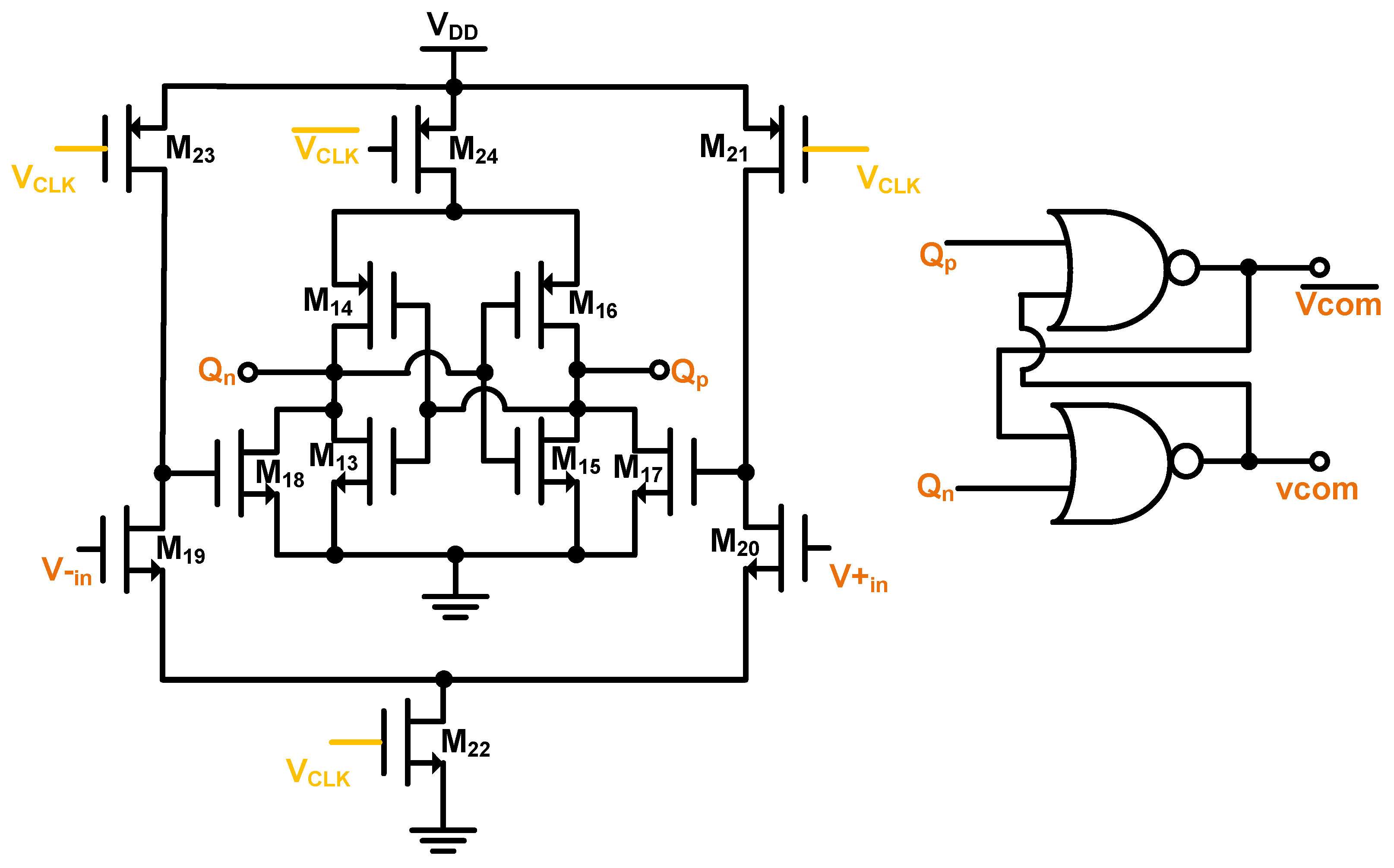
2.3. Programmable Current Matching and Minimum Voltage Selector Circuitry
Different topologies are employed for current sinks, such as single-transistor or Cascode current mirror [4]. The single-transistor current mirror suffers from low output impedance, making it less accurate as a current sink for WLED driver applications. On the other hand, the Cascode structure improves the accuracy by increasing output impedance; it requires a higher overhead voltage. This results in more power consumption and, hence, degrades the system efficiency.
The top part of Figure 5 shows the proposed programmable current matching circuit. This circuit consists of three programmable current sinks, one per string. The current sink comprises a boosting amplifier (), current sink transistor M1, and a digital programable resistor bank. The current sink value is made programmable as the reference voltage () and the programmed resistor values are adjustable. With high gain boosting amplifiers (), the voltage at the source of the transistor should closely equal the reference voltage ; hence, the current value approaches . For this condition to be satisfied, the current sink transistor M1 must operate in the saturation region. To maintain M1 in the saturation region, the drain potential of M1 should be higher than , which is equal to plus the overdrive voltage of M1. Once the drain voltage of M1 reaches the set value , the digital comparator () triggers low. At this point, both the targeted voltage and current values are met.
Figure 5.
The proposed programmable current matching with minimum voltage selector circuitry.
The resistance value is selected based on a five-bit digital code . Since the number of segments is 25, only 25 out of 32 () combinations are used. The resistor values are chosen such that, when divided by the reference voltage , the current is a multiple of 1 mA.
The minimum voltage selector in the proposed circuit is comprised of three digital comparators with output terminals wired to a three-input NOR gate. The drain voltage of each sink transistor is compared to a 300 mV reference voltage () to ensure a high enough voltage for full activation of the WLEDs. A detailed design of the comparators’ circuitry can be found in [24]. These three digital comparators are of clocked-latch type, also known as double-tail comparators, as depicted in Figure 6. Unlike the traditional four-stack comparator, e.g., [25,26], this comparator has three stacks of MOS transistors which allows it to operate under lower supply voltage. This structure is intended for ultra-low power operation (i.e., zero static power consumption) and not necessarily high performance. The same clock used to generate the switching frequency is used to drive the double-tail comparators, which eliminates the need for a dedicated clock signal. Each comparator is triggered by the clock to sample and the corresponding drain voltage of the current sink transistor. As shown in Figure 6, the second stage of that comparator consists of two NOR-Gate latches to sharpen the output edges. The output () of theses comparators are used as the input of the NOR1 gate.
Figure 6.
Double-tail comparator circuitry.
To ensure all strings are active, the sink transistors’ drain voltages should be higher than their respective . Under this condition, the comparators’ outputs are all zero, and, thus, the NOR1 gate output triggers high. So long as the comparator’s output is non-zero, the corresponding string connected to it has not yet activated; thus, the needs to be increased. Consequently, the loop keeps increasing the duty cycle until each comparator’s output reaches zero. The NOR gate logic was selected over NAND gate logic due to its size and speed superiority in CMOS technology [27].
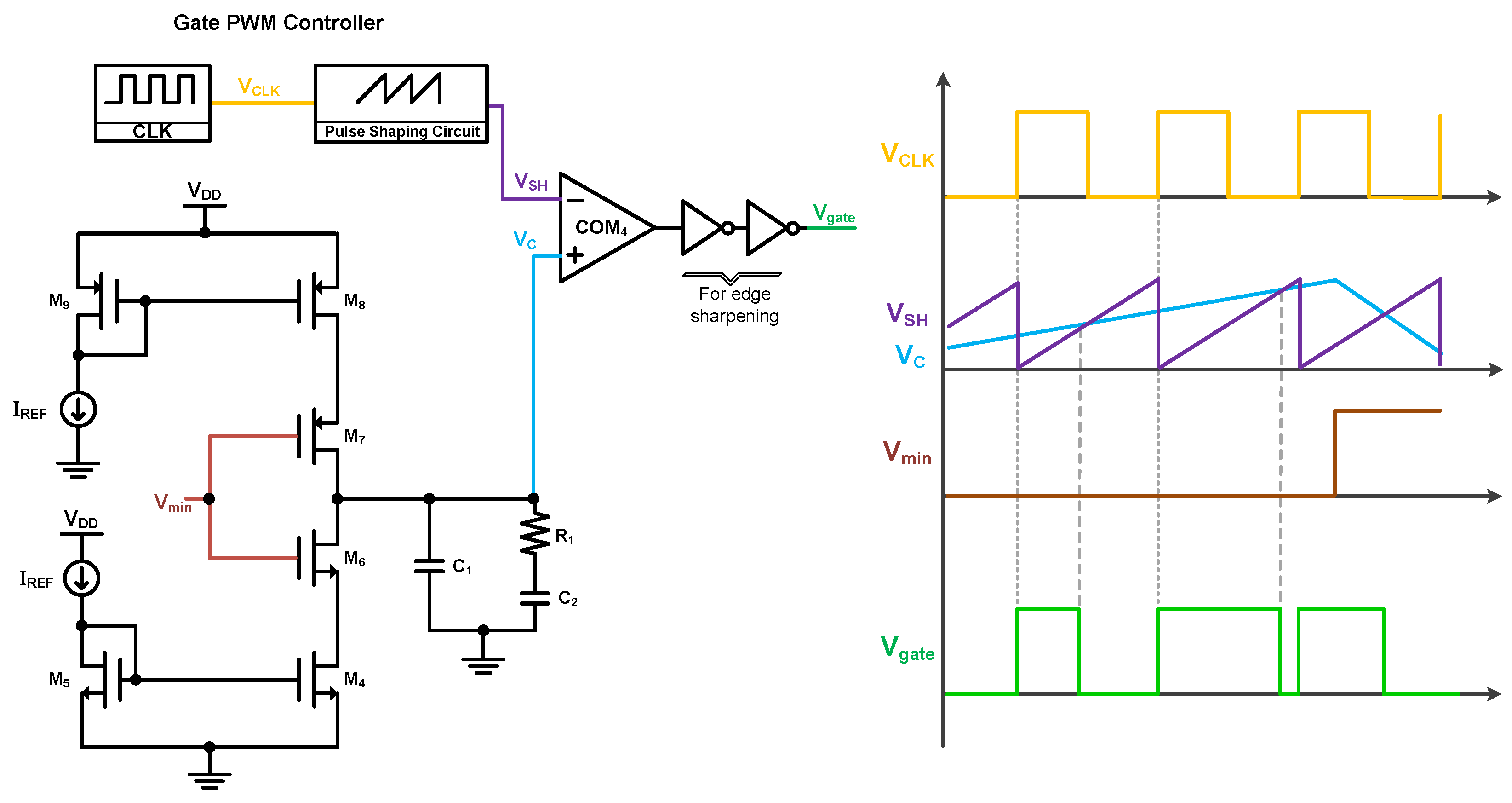
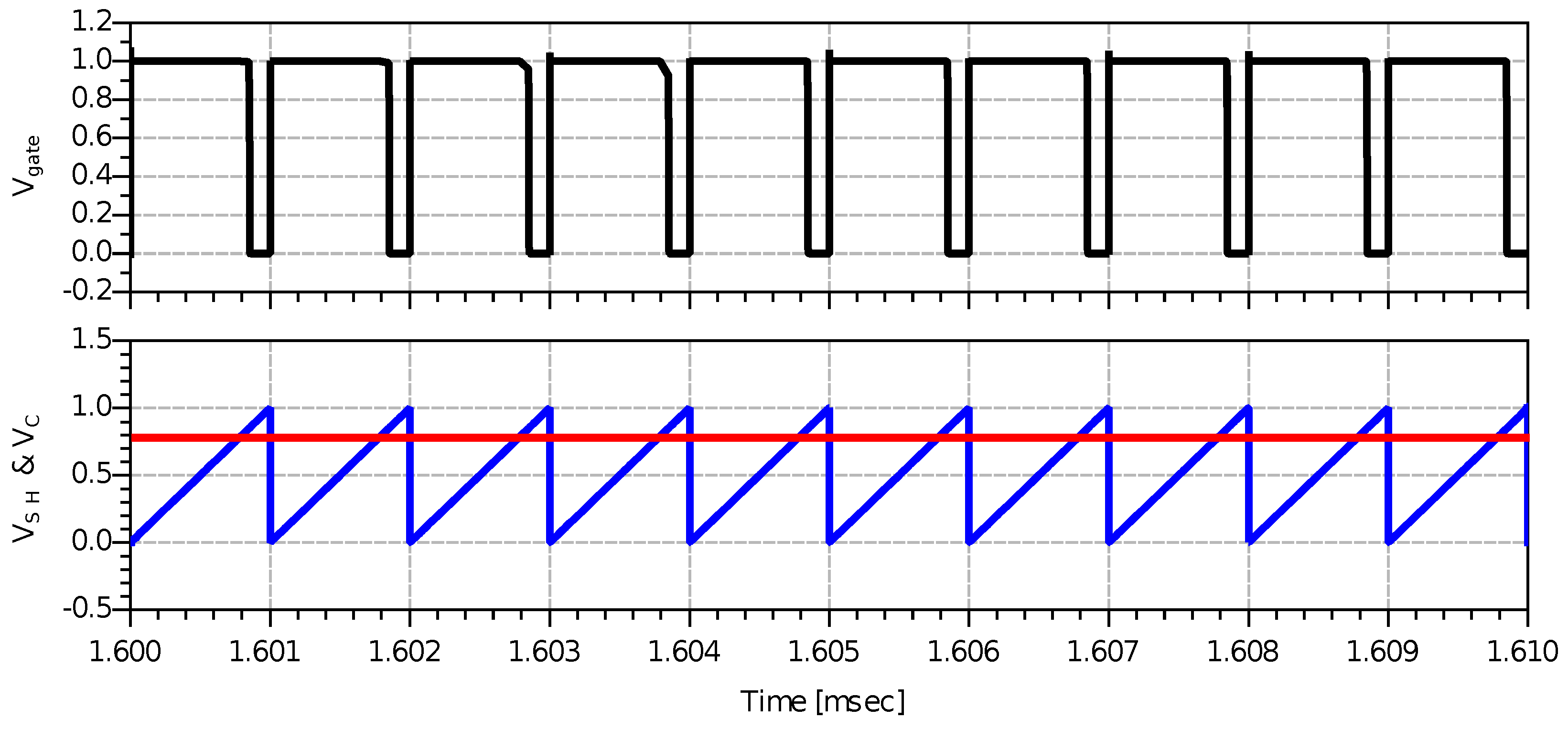
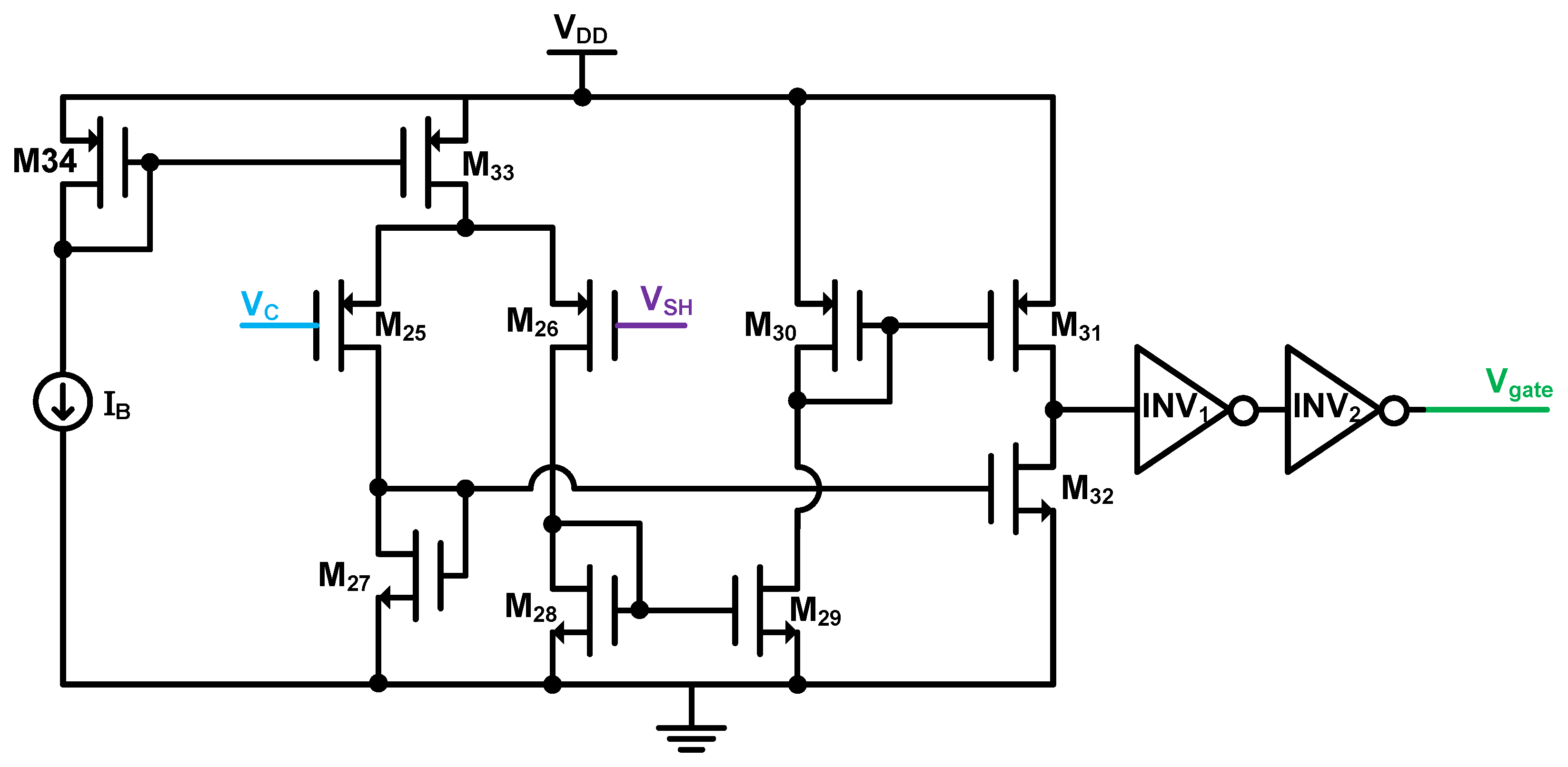
2.4. Compensator and PWM Modulator Circuitry
The compensator circuit consists of a charge pump and a loop filter to stabilize the system. The output of the compensator , when compared to the sawtooth signal , generates a duty cycle signal that drives the main switch of the power stage.
Figure 7 shows the implementation of the compensator and PWM modulator along with the generated waveforms at selected nodes. The charge pump is composed of a current sink (M4) and current source (M8), as well as two switch transistors (M6 and M7). As the switch M7 turns ON, the current source transistor M8 pumps current to the output loop filter (C1, C2, and R), consequently raising its output voltage. The current sink transistor M4 does the opposite when switch M6 turns ON. Since is a binary signal, either the current source or the current sink can be ON at any time. The charge pump integrates the pulses to a continuous output signal . Then, it is compared to the one-sided sawtooth signal generated by the pulse shaping circuit. While the loop filter capacitor (C1) serves as an integrator to help stabilize the system, the R1&C2 branch adds a zero to the compensation circuit to improve the phase margin of the system. The inverters in front of the comparator are used to sharpen the edges of the drive signal. Note that this charge bump and the loop filter combination acts as a type-II compensator in this implementation.
Figure 7.
Proposed pulse shaping and compensator circuit with generated waveform at selected nodes.
The comparator (COM4) shown in Figure 7 cannot be of a clocked-latch type comparator as the has the same clock signal frequency. Therefore, push-pull output comparator topology is used to design COM4 [28], as shown in Figure 8.
Figure 8.
The push-pull output comparator circuit.
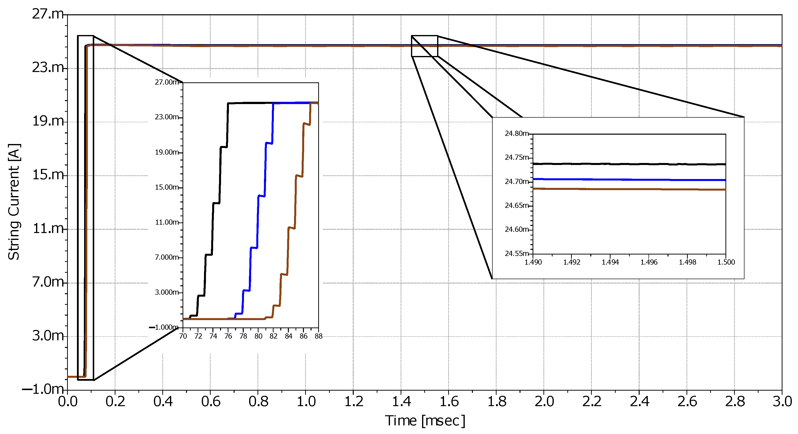
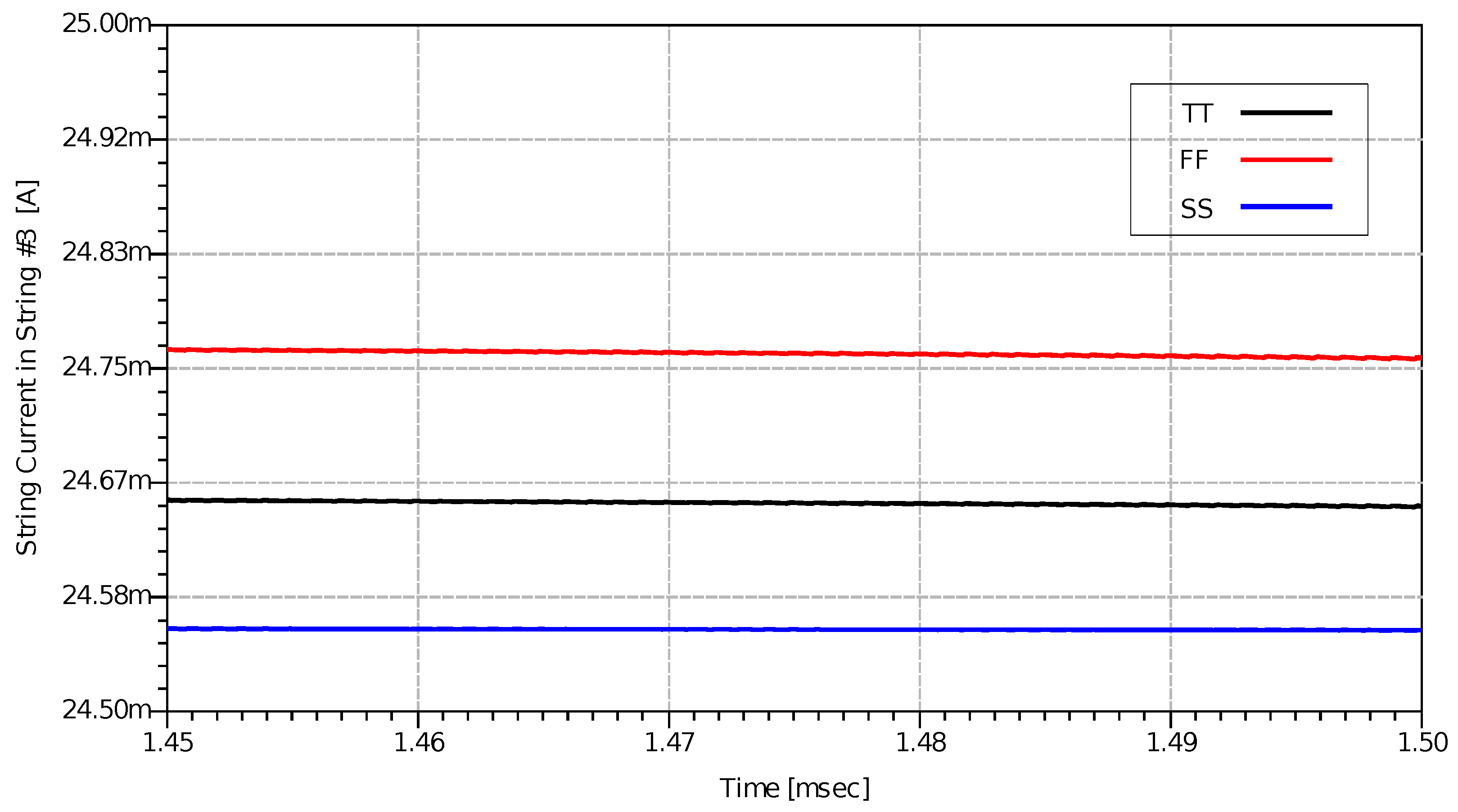
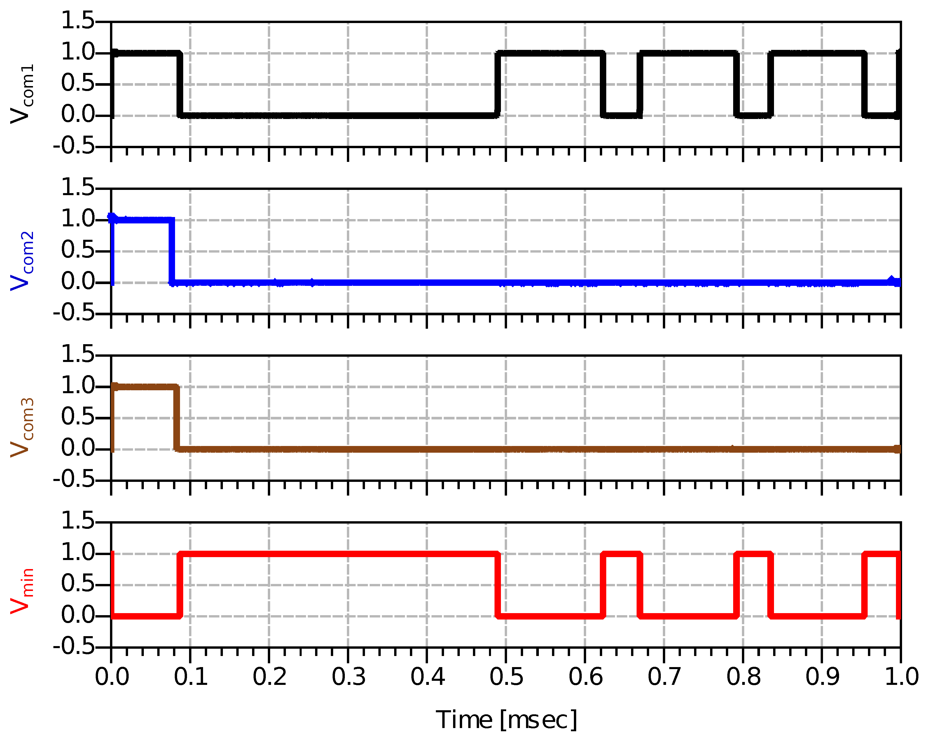
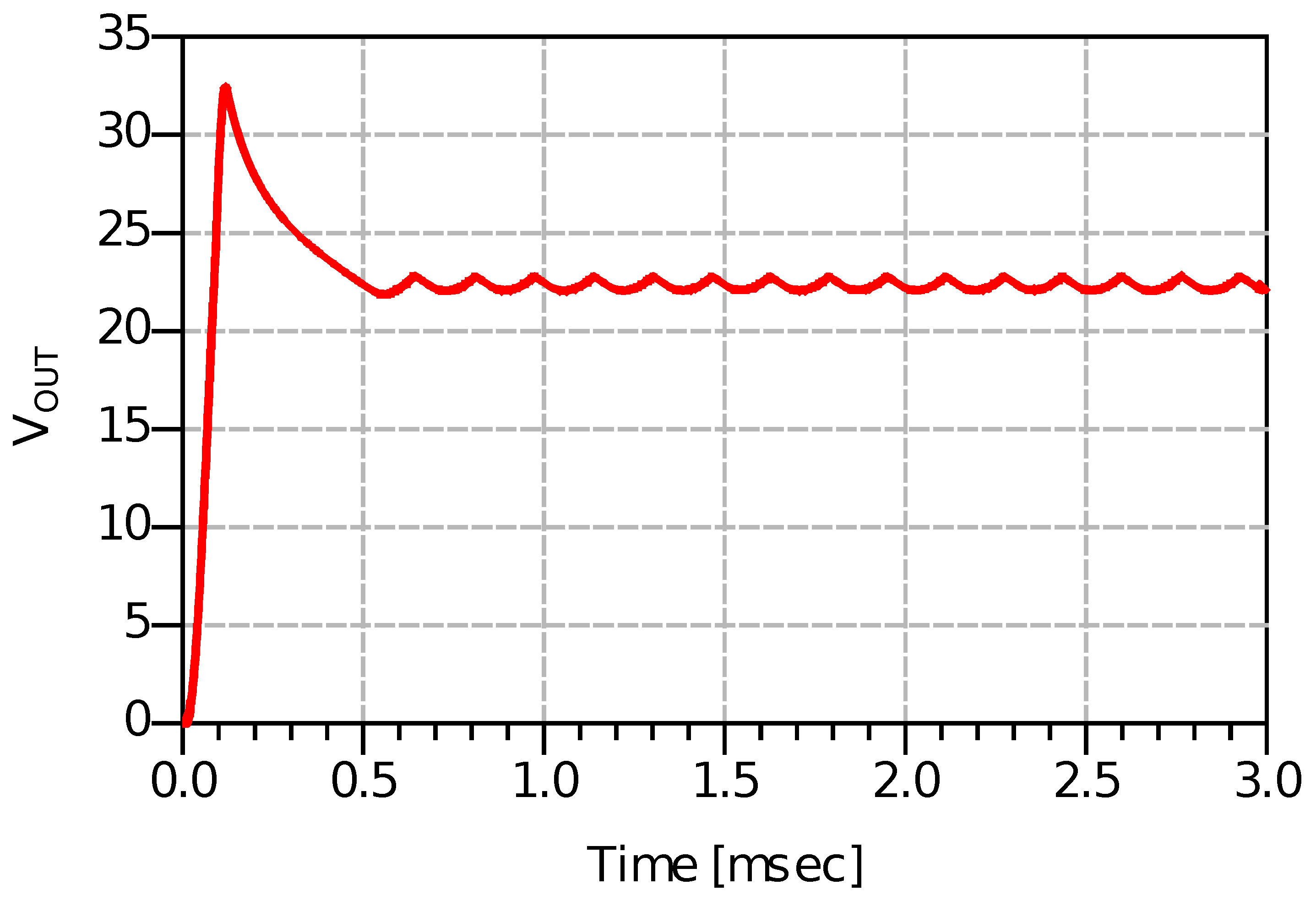
3. Simulation Results
The proposed circuit was simulated with ADS CAD tools. A standard 40nm 1P9M CMOS process has been used. To verify the proposed circuit’s functionality, WLED (NSSW088AT) has been used [21]. The WLED has a typical forward voltage of 3.2 V with a tolerance of (). The forward voltage drop in each WLED has been selected to represent the worst-case scenario where a mismatch between strings is maximized. The arrangement is comprised of three strings; each has six WLEDs. In string #1, the VF was set to the maximum possible value of 3.5 V, while, in the second string, each WLED has the minimum possible of 2.8 V. WLEDs in the third string each have equal to the typical value of 3.2 V.
Figure 9 shows the output voltage () waveform of the boost converter. The voltage level is set by the controller based on the minimum current sink overhead (), as shown in Figure 5. This minimum voltage satisfies all the WLEDs in all strings, including the one with the highest combination of (i.e., string #1). The output voltage ripple in a steady-state is a result of the single-bit feedback controller presented at the output of the NOR gate. This ripple has no effect on the current accuracy of the individual string due to the proposed current sink topology. In this current sink, the current is a weak function of the drain-source voltage () of the current sink transistor. The string current is mainly set by the voltage reference () that is independent of the output voltage ripple.
Figure 9.
The common-output voltage of the WLED drives .
As the targeted minimum output voltage has been reached, all strings are being activated and operational. This is clearly illustrated in Figure 10, where the individual currents in each string have reached their targeted value of 25 mA in a steady state. The zoomed-in region in Figure 10 shows the steady-state current of each string. The error in the steady-state current of string #1 (24.785 mA) is due to the finite gain of the boosting amplifier used in the current sink (i.e., , , and shown in Figure 5). The currents in string #2 and #3 exhibit the same behavior. The total forward voltage drops of the WLED in the string dictate the overdrive voltage of the current sink transistor () of a particular string. Therefore, the higher the overdrive voltage, the higher the string current, as shown in Figure 1 for strings #2. The string current, including the effect of process corner variation ( TT, SS, and FF), is depicted in Figure 11. The results clearly show the minimal effect of process corners on the accuracy of the current value.
Figure 10.
The waveforms of strings’ currents.
Figure 11.
The effect of process corner variation on the string current.
Figure 12 shows the output of the digital comparator of the three strings along with the NOR1 gate output. belongs to the string with the highest total forward voltage (i.e., string #1) that determines the duty cycle. As the output voltage reaches the needed value to activate all strings, the feedback signal starts toggling between 1 and 0 due to the fact that the digital comparator (COM1) acts as a single-bit analog-to-digital converter. A 1-bit ADC causes the output voltage to ripple. The proposed current sink topology makes it immune to the fluctuation (ripple) of the output voltage. Unlike , the digital comparator output signals and are low, as the overhead voltage across the corresponding current sinks has exceeded the reference voltage ().
Figure 12.
Digital comparators and NOR1 gate output waveforms.
Figure 13 depicts the duty cycle () signal being generated from the single-sided sawtooth signal () and the control signal (). The duty cycle is determined by comparing the control signal (positive terminal of the comparator) to the sawtooth signal (negative terminal of the comparator). The period of the sawtooth signal matches the switching frequency period (i.e., the ).
Figure 13.
Close-up view of duty cycle () signal being generated from the single-sided sawtooth signal () and the control signal ().
Table 2 compares the key features of the proposed design with the state-of-the-art SIMO drivers. The proposed design exhibits a superior inter-strings current matching accuracy, owing to the programable resistor current sink topology. The proposed on-chip programable resistor reduces the component count compared to the external resistance solutions [5,7,29] and reduces the current sensing complexity [30]. This results in a lower power consumption and a simpler dimming scheme. With the individual programming of the current sink resistor, independent string current dimming is achievable. Unlike the PWM dimming technique that requires an extra clock signal that is different from the main switch frequency, this work relies on a clock-less digitally controlled dimming strategy.
Table 2.
Performance summary and comparison with the state-of-the-art.
The on-chip implementation of the current sensing and the control circuitries permits high switching frequencies and, thus, reduces the size of the passive components of the power stage. Therefore, the switching frequency of 1 MHz has been used in this design. Based on the prior art list in Table 2, the proposed solution uses a nanometer process node that is more suitable for implementations with heavy digital content.
In summary, the proposed WLED driver possesses the highest inter-strings current matching accuracy, the most advanced process technology, and the best individual brightness/dimming functionality. The switching frequency is among the highest in the reviewed literature. The proposed architecture offers an excellent choice for WLED driver design when all key features are considered.
4. Conclusions
This paper investigates various essential features and design aspects of a single-inductor, common-output, and multi-string WLED driver for low-power portable devices. A boost converter-based WLED driver has been implemented and simulated using 40 nm 1P9M TSMC CMOS technology. The proposed design exhibits high efficiency and a programmable current sink. Furthermore, the design mitigates the inherent low on-resistance of the advanced nano-meter process node. The proposed design shows high inter-string current accuracy of 0.2% by sensing the overhead voltage across the amplifier-boosted single transistor current sink. The sensed voltage is compared with a fixed reference value of 300 mV to maintain low power dissipation for the programmable current sink circuit. Unlike the variable reference voltage control scheme, the programmable resistor has a fixed power dissipation despite the change in programmed current value due to dimming requirements. This programmable current sink accurately adjusts the string current by a 1 mA step with a maximum of 25 mA. The designed WLED driver supports a battery level input voltage of 3.2–4.2 V and an output voltage up to 25 V. A three-string, each with six WLEDs, arrangement has been proved to be the most efficient arrangement among all possible combinations for an 18-WLED backlight system, with a reported peak efficiency of 91%. The 40 nm process has a very high unity-gain frequency ( = 465 GHz), which supports a higher switching frequency. Therefore, a switching frequency of 1 MHz was used to implement WLED driver circuitry. This reduces the size of the passive element in the power stage.
Author Contributions
Conceptualization, F.R.S.; methodology, F.R.S., H.H.A. and I.A.; software, F.R.S.; validation, H.H.A., F.R.S. and I.A.; writing—original draft preparation, H.H.A., F.R.S. and I.A.; writing—review and editing, H.H.A., F.R.S. and I.A. All authors have read and agreed to the published version of the manuscript.
Funding
This research received no external funding.
Data Availability Statement
The data presented in this study are available in article.
Acknowledgments
The authors would like to thank EUROPRACTICE for their kind support by providing the technology files.
Conflicts of Interest
The authors declare no conflict of interest.
Abbreviations
The following abbreviations are used in this manuscript:
| CMOS | Complementary metal–oxide–semiconductor |
| WLED | White Light-Emitting Diode |
| CCM | Continuous Conduction Modes |
| DCM | Discontinuous Conduction Modes |
References
- Ahmad, H.H.; Shahroury, F.R. Design of a High Efficiency WLED Driver in 40 nm CMOS Technology. In Proceedings of the 2020 32nd International Conference on Microelectronics (ICM), Aqaba, Jordan, 14–17 December 2020; pp. 1–4. [Google Scholar]
- Eguchi, K.; Shibata, A.; Do, W.; Asadi, F. An LED driver connecting a nested-type SC converter and an SI buck-boost converter in parallel. In Proceedings of the 2021 3rd Asia Energy and Electrical Engineering Symposium (AEEES), Chengdu, China, 26–29 March 2021; pp. 255–258. [Google Scholar]
- Branas, C.; Azcondo, F.J.; Alonso, J.M. Solid-state lighting: A system review. IEEE Ind. Electron. Mag. 2013, 7, 6–14. [Google Scholar] [CrossRef]
- Ahmad, H.H.; Shahroury, F.R.; Abuishmais, I. A Multi-Output Multi-String High-Efficiency WLED Driver Using 40 nm CMOS Technology. J. Low Power Electron. Appl. 2021, 11, 47. [Google Scholar] [CrossRef]
- Kim, H.C.; Yoon, C.S.; Jeong, D.K.; Kim, J. A single-inductor, multiple-channel current-balancing LED driver for display backlight applications. IEEE Trans. Ind. Appl. 2014, 50, 4077–4081. [Google Scholar] [CrossRef]
- Han, H.; Zhang, F.; Liu, M. PWM dimming method for capacitor-clamped current-sharing circuit in LED backlight system. IEEE J. Emerg. Sel. Top. Power Electron. 2018, 6, 1190–1197. [Google Scholar] [CrossRef]
- Guo, Y.; Li, S.; Lee, A.T.L.; Tan, S.; Lee, C.K.; Hui, S.Y.R. Single-Stage AC/DC Single-Inductor Multiple-Output LED Drivers. IEEE Trans. Power Electronics 2016, 31, 5837–5850. [Google Scholar] [CrossRef]
- Kang, E.C.; Yeon, J.E.; Kim, D.S.; Kwon, D. Sequential low-voltage detecting method for multistring LED BLU circuit. Electron. Lett. 2010, 46, 839–840. [Google Scholar] [CrossRef]
- Wang, Y.; Qi, N.; Guan, Y.; Cecati, C.; Xu, D. A single-stage LED driver based on SEPIC and LLC circuits. IEEE Trans. Ind. Electron. 2016, 64, 5766–5776. [Google Scholar] [CrossRef]
- Reddy, U.R.; Narasimharaju, B. A cost-effective zero-voltage switching dual-output led driver. IEEE Trans. Power Electron. 2016, 32, 7941–7953. [Google Scholar] [CrossRef]
- Hwu, K.I.; Jiang, W.Z. Input-current-ripple-free two-channel LED driver. IEEE Trans. Ind. Electron. 2016, 64, 5865–5874. [Google Scholar] [CrossRef]
- Doshi, M.; Zane, R. Digital architecture for driving large LED arrays with dynamic bus voltage regulation and phase shifted PWM. In Proceedings of the APEC 07-Twenty-Second Annual IEEE Applied Power Electronics Conference and Exposition, Anaheim, CA, USA, 25 February–1 March 2007; pp. 287–293. [Google Scholar]
- Hong, S.i.; Han, J.W.; Kim, D.H.; Kwon, O.K. A double-loop control LED backlight driver IC for medium-sized LCDs. In Proceedings of the 2010 IEEE International Solid-State Circuits Conference-(ISSCC), San Francisco, CA, USA, 7–11 February 2010; pp. 116–117. [Google Scholar]
- Oh, T.J.; Cho, A.; Ki, S.L.; Hwang, I.C. A low-power and low-cost digitally-controlled boost LED driver IC for backlights. In Proceedings of the 2012 IEEE Asian Solid State Circuits Conference (A-SSCC), Kobe, Japan, 12–14 November 2012; pp. 237–240. [Google Scholar]
- Zhang, H.J. Basic Concepts of Linear Regulator and Switching Mode Power Supplies. Available online: https://www.analog.com/en/app-notes/an-140.html (accessed on 2 December 2021).
- Burgyan, L.; Prinz, F. High Efficiency LED Driver. U.S. Patent 6,690,146, 10 February 2004. [Google Scholar]
- Modepalli, K.; Parsa, L. A scalable N-color LED driver using single inductor multiple current output topology. IEEE Trans. Power Electron. 2015, 31, 3773–3783. [Google Scholar] [CrossRef]
- Hiramoto, T. Five nanometre CMOS technology. Nat. Electron. 2019, 2, 557–558. [Google Scholar] [CrossRef]
- Bianchi, R.; Monsieur, F.; Blanchet, F.; Raynaud, C.; Noblanc, O. High voltage devices integration into advanced CMOS technologies. In Proceedings of the 2008 IEEE International Electron Devices Meeting, San Francisco, CA, USA, 15–17 December 2008; pp. 1–4. [Google Scholar]
- Erickson, R.W.; Maksimovic, D. Fundamentals of Power Electronics, 3rd ed.; Springer: Berlin/Heidelberg, Germany, 2020. [Google Scholar]
- NICHIA Corporation. Specification for White LED; Cat. No. 201008; NICHIA Corporation: Tokushima, Japan, 2019. [Google Scholar]
- Yao, K.; Moyer, J.C. Control of Multi-String LED Array. U.S. Patent 8,410,716, 4 February 2013. [Google Scholar]
- Hsieh, Y.T.; Liu, B.D.; Wu, J.F.; Fang, C.L.; Tsai, H.H.; Juang, Y.Z. A high-dimming-ratio LED driver for LCD backlights. IEEE Trans. Power Electron. 2012, 27, 4562–4570. [Google Scholar] [CrossRef]
- Schinkel, D.; Mensink, E.; Klumperink, E.; Van Tuijl, E.; Nauta, B. A double-tail latch-type voltage sense amplifier with 18ps setup+ hold time. In Proceedings of the 2007 IEEE international solid-state circuits conference. Digest of technical papers, San Francisco, CA, USA, 11–15 February 2007; pp. 314–605. [Google Scholar]
- Nikolic, B.; Oklobdzija, V.G.; Stojanovic, V.; Jia, W.; Chiu, J.K.S.; Leung, M.M.T. Improved sense-amplifier-based flip-flop: Design and measurements. IEEE J. Solid-State Circuits 2000, 35, 876–884. [Google Scholar] [CrossRef]
- Wicht, B.; Nirschl, T.; Schmitt-Landsiedel, D. Yield and speed optimization of a latch-type voltage sense amplifier. IEEE J. Solid-State Circuits 2004, 39, 1148–1158. [Google Scholar] [CrossRef]
- Sedra, A.; Smith, K.; Carusone, T.C.; Gaudet, V. Microelectronic Circuits 8th Edition. Chapter 2020, 14, 1235–1236. [Google Scholar]
- Allen, P.E.; Holberg, D.R. CMOS Analog Circuit Design; Elsevier: Amsterdam, The Netherlands, 2011. [Google Scholar]
- Yang, W.H.; Yang, H.A.; Huang, C.J.; Chen, K.H.; Lin, Y.H. A high-efficiency single-inductor multiple-output buck-type LED driver with average current correction technique. IEEE Trans. Power Electron. 2017, 33, 3375–3385. [Google Scholar] [CrossRef]
- Qu, Y.; Wang, Z. Soft-switching techniques for single-inductor multiple-output led drivers. IEEE Trans. Power Electron. 2020, 35, 13748–13756. [Google Scholar] [CrossRef]
Publisher’s Note: MDPI stays neutral with regard to jurisdictional claims in published maps and institutional affiliations. |
© 2022 by the authors. Licensee MDPI, Basel, Switzerland. This article is an open access article distributed under the terms and conditions of the Creative Commons Attribution (CC BY) license (https://creativecommons.org/licenses/by/4.0/).