Article

Design of In-Memory Parallel-Prefix Adders

Chair of Computer Architecture, Friedrich-Alexander-Universität Erlangen-Nürnberg (FAU), 91058 Erlangen, Germany
J. Low Power Electron. Appl. 2021, 11(4), 45; https://doi.org/10.3390/jlpea11040045
Submission received: 14 October 2021 / Revised: 5 November 2021 / Accepted: 17 November 2021 / Published: 24 November 2021
(This article belongs to the Special Issue Low Power Memory/Memristor Devices and Systems)

Abstract

:
Computational methods in memory array are being researched in many emerging memory technologies to conquer the ‘von Neumann bottleneck’. Resistive RAM (ReRAM) is a non-volatile memory, which supports Boolean logic operation, and adders can be implemented as a sequence of Boolean operations in the memory. While many in-memory adders have recently been proposed, their latency is exorbitant for increasing bit-width ( O ( n ) ). Decades of research in computer arithmetic have proven parallel-prefix technique to be the fastest addition technique in conventional CMOS-based binary adders. This work endeavors to move parallel-prefix addition to the memory array to significantly minimize the latency of in-memory addition. Majority logic was chosen as the fundamental logic primitive and parallel-prefix adders synthesized in majority logic were mapped to the memory array using the proposed algorithm. The proposed algorithm can be used to map any parallel-prefix adder to a memory array and mapping is performed in such a way that the latency of addition is minimized. The proposed algorithm enables addition in O ( l o g ( n ) ) latency in the memory array.

1. Introduction

Conventional computer architecture is facing an acute problem—the ‘von Neumann bottleneck’ or ‘memory wall’. The shuffling of data between processing and memory units is energy-consuming and time-consuming and degrades the performance of contemporary computing systems [1,2]. In other words, the energy needed to move data (between memory and processing units) forms a significant portion of the computational energy. To overcome the memory wall, the processor and memory unit must be brought closer to each other. A 3D stacking of DRAM dies over logic die, often referred to as near-memory computing [3], was pursued earlier to reduce the latency and energy for data movement between processor and memory. The recent trend is to move computing to the location of the data, i.e., in-memory computing.
In in-memory computing, the data are processed at their location (i.e., in the memory array) and not moved out of the memory array to a separate processing unit. At present, diverse operations from arithmetic operations to cognitive tasks such as machine learning and pattern recognition are being explored in memory arrays [4]. This article focuses on arithmetic operations and how adders can be implemented in memory. It should be noted that in-memory computing is pursued in many memory technologies—both conventional (SRAM, DRAM) and emerging non-volatile memories (Resistive RAM, STT-MRAM, PCM, FeFET). However, in this article, we restrict our focus to Resistive RAM technology to achieve a greater focus on the design of parallel-prefix adders. Resistive RAM device is a two-terminal Metal–Insulator–Metal structure in which data can be stored as resistance. A positive voltage across the structure forms a conductive filament (low resistance state) and a negative voltage ruptures the filament (high resistance state), leading to two stable resistances. Boolean gates can be implemented in the memory array by altering the structure of the memory array, the peripheral circuitry around the array, or both. Arithmetic circuits such as adders can be implemented as a chain of such Boolean operations.
Although different in-memory adders have been proposed in the literature, the latency of in-memory adders is a severe disadvantage in in-memory computing, i.e., an addition operation needs a long sequence of Boolean operations. A poorly optimized in-memory adder may take longer to compute (add two n-bit numbers) than the combined time it takes to fetch data from memory and add them in a CMOS-based processor. In a computing system, adders constitute the basic computational unit. In-memory adders have not had their latency studied and optimized for an increasing bit-width (n-bit operand). In practice, 32-bit/64-bit in-memory adders require hundreds of cycles due to O ( n ) latency requirements. It was originally proposed that parallel-prefix (PP) adders could bring down the latency caused by the rippling of carry in CMOS-based adders. PP adders are the fastest adders in conventional CMOS technology [5,6]. To improve the latency of in-memory adders, it is necessary to learn lessons from the decades of research on CMOS adders and adopt them for in-memory addition. Therefore, parallel-prefix adders were pursued in this work to improve the latency of in-memory adders. More specifically, we propose a generic methodology to design any PP adder in memory. As an example, we consider the Ladner–Fischer type of PP adder and demonstrate how this can be implemented in-memory in O ( l o g ( n ) ) latency. The presented method requires no major modifications to the peripheral circuitry of the memory array and is also energy-efficient.
The rest of the paper is organised as follows. Section 2 reviews the state-of-the-art in-memory adders and classifies in-memory adders on the basis of state fullness, logic primitive and architecture. The review identifies the exorbitant latency of adders with increasing bit-width, as a significant issue that needs attention. Section 3 presents PP adders as a solution to the long latency incurred by the rippling of carry. Section 4.1 reviews the in-memory majority gate, which is the fundamental logic gate used in this work to implement the PP adder in the memory array. Section 4.2 elaborates how PP adders can be synthesized using majority logic. Having synthesized PP adders in majority logic, Section 4.3.3 elaborates how they can be mapped to the memory array. We present the simulation methodology in Section 5.1. In Section 5.2, we analyse how the latency of the proposed adder grows with increasing bit-width. Section 5.3 and Section 5.4 analyse how the energy and area of the proposed adder grow with increasing bit-width. In Section 5.5, we compare the proposed adder with other adders reported in the literature, followed by the Conclusion in Section 6.

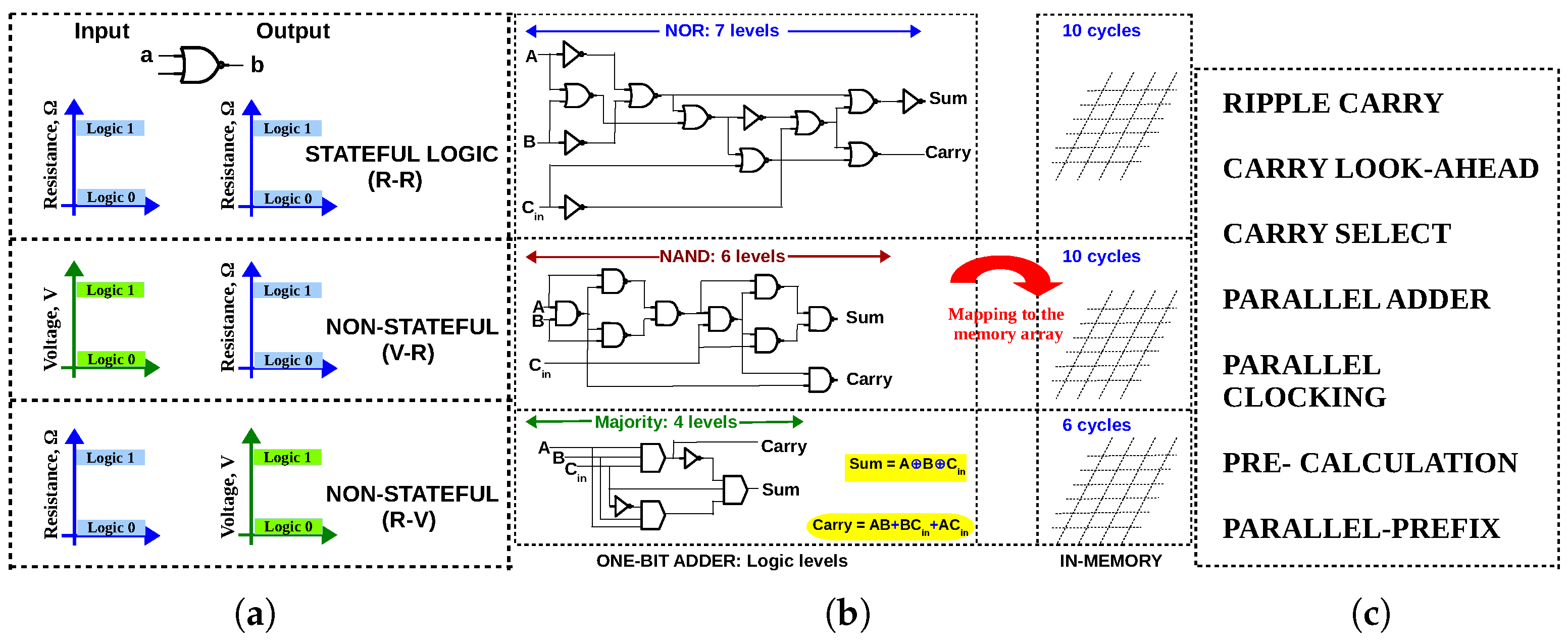
2. In-Memory Adders: A Brief Review

Conventionally, adders were designed using logic gates built from CMOS transistors. In contrast, an in-memory adder is designed using a ‘functionally complete’ Boolean logic primitive. NOR, for example, is functionally complete, since any Boolean logic can be expressed using NOR gates. Therefore, if an NOR gate can be implemented in the memory array, any arithmetic circuit can be implemented in the memory array. NAND, IMPLY + FALSE [7] and Majority + NOT [8] are other functionally complete logic primitives. In the last 5 years, several in-memory adders have been proposed. They can be classified as the following:
  • State variable used for computation—stateful or non-stateful;
  • Logic primitive used for computation—NAND or NOR or IMPLY or MAJORITY or XOR or a combination of these;
  • Adder architecture—how is the carry propagated?
Stateful in-memory adders perform an addition by logic gates, where each gate is executed by manipulating the resistance of a memristor (i.e., the internal state) rather than by a mix of resistance and voltage [9]. If voltage is also used, in addition to resistance, the logic gate and the adder are said to be non-stateful (Figure 1a). This is one of the characteristics of in-memory adders that, with certain modifications to conventional memory, a particular logic primitive can be realized and other logic primitives need to be realized in terms of this logic primitive. The NOR-based memristive logic family (MAGIC), for example, requires that all other gates (AND, OR, XOR) are expressed in terms of NOR gates and then used in the memory array. Similarly, in the NAND-based adder reported in [10], an XOR gate is implemented as NAND gates (one XOR requires four memory cycles). Figure 1b illustrates a one-bit full adder expressed solely as NOR/NAND/Majority gates (expressing a circuit using single logic primitive is preferred for in-memory implementation). Finally, an issue that is often overlooked in this emerging area is the issue of carry-propagation. The manner in which carry is propagated from LSB to MSB decides the speed of the in-memory adder. In the in-memory community, different adder architectures, from ripple carry (slowest) to parallel-prefix (fastest) adders, have been proposed.
Table 1 lists different in-memory adders that have been reported recently and their latency for 8-bit and n-bit. The adders are also classified based on the three characteristics we reviewed—state variable, logic primitive and adder architecture. A key observation is that logic primitive plays an important role in determining the latency. IMPLY is a weak logic primitive, and generally incurs more latency than all other logic primitives. XOR and the majority are generally stronger logic primitives than OR/AND/NOR. This is evident from the fact that XOR-based and majority-based ripple-carry adders are faster than NAND/NOR-based ripple-carry adders [13]. In other words, with the adder configuration being the same (ripple-carry), logic primitive plays an important role in determining the latency of in-memory addition. Another important finding is that the adder architecture plays a key role in deciding the latency for increasing bit-width. This is evident from the latency of OR + AND-based adders in Table 1. Both adders used the same logic primitive (OR + AND), but [14] uses ripple-carry architecture, achieving a latency of 6n + 1 while [15] uses a parallel-prefix configuration to achieve a latency of 8 l o g 2 ( n ) + 13. As an example, a 32-bit adder based on OR + AND logic will require 193 cycles and 53 cycles for ripple-carry and parallel-prefix architectures, respectively. Hence, for larger bit-widths, architecture (carry propagation technique) plays an important role in latency. In summary, both adder architecture and logic primitive influence the latency of in-memory adder. Therefore, majority logic primitive and parallel-prefix adder architecture were chosen in this work to drastically minimize the latency of in-memory adders.

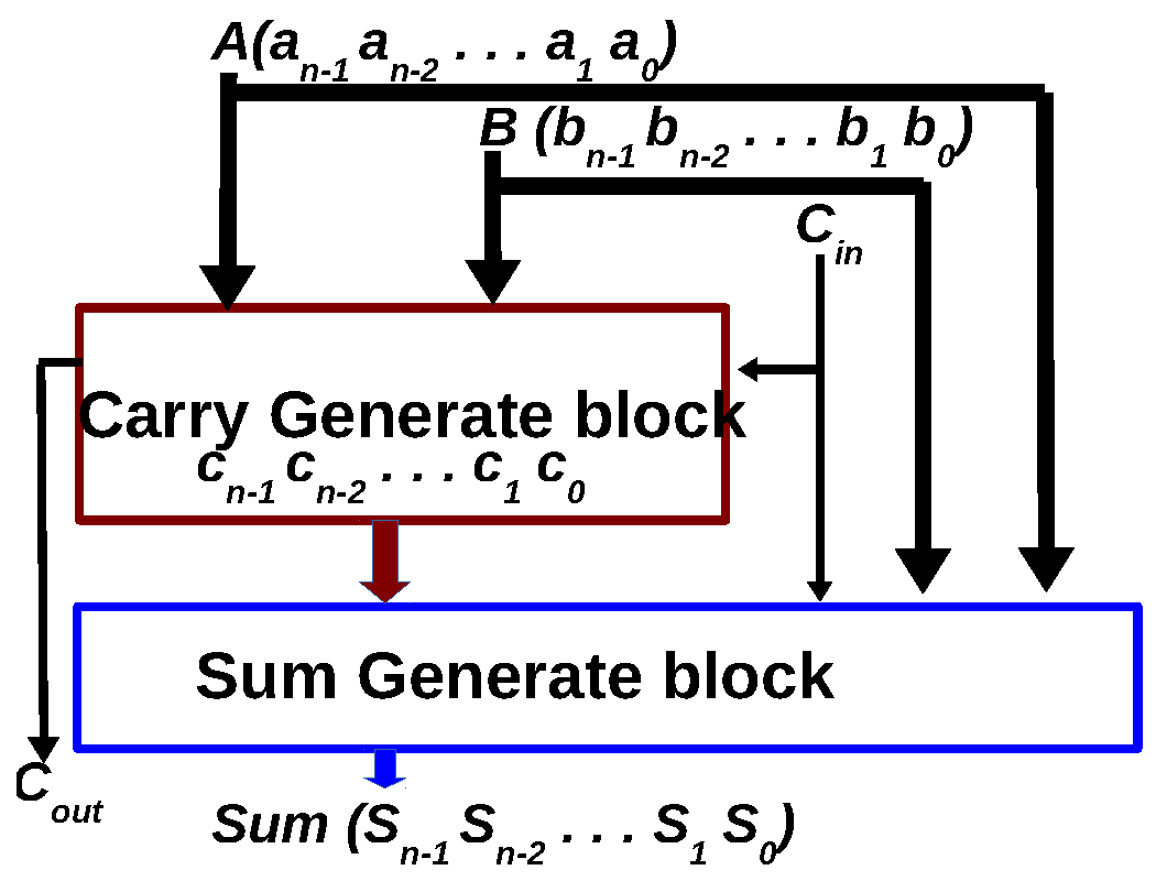
3. Parallel-Prefix Adders: A Solution for the Carry-Propagation Problem

When two n-bit binary numbers A ( a n 1 a n 2 · a 0 ) and B ( b n 1 b n 2 · b 0 ) are added, the sum bit S i at the ith bit position is computed as,
S i = H i C i 1
where, H i = A i B i and C i 1 is the carry computed in the previous bit position. To compute the sum bits of the next significant bit position, the incoming carry C i 1 is propagated to the next position. This is accomplished using carry generate bits ( G i = A i · B i ) and carry propagate bits ( P i = A i + B i ). The carry-out ( C i ) of a particular bit position is always a function of the carry from the previous bit ( C i 1 ), and they are expressed as follows:
C i = G i + P i · C i 1
Thus, during the 8-bit addition of a 7 a 6 a 5 a 4 a 3 a 2 a 1 a 0 and b 7 b 6 b 5 b 4 b 3 b 2 b 1 b 0 , sum bit S 6 = H 6 C 5 and C 5 is a function of a 5 , b 5 , C 4 according to Equations (1) and (2). In other words, S 6 cannot be computed until C 5 is computed, which recursively depends on the carry-out of the lower significant bit. This is the decades old carry-propagation problem and significantly affects the speed of n-bit addition as n grows. Ripple-carry adders are extremely slow for 32-bit/64-bit addition due to this carry propagation. To improve this situation, carry-skip adders were proposed, which allowed for carries to skip across block of bits instead of rippling through them. This was followed by Carry-lookahead adders, where carries were computed in parallel and achieved logarithmic logic depth [26]. Parallel-prefix (PP) adders improved on the carry-look ahead adder by expressing carry-propagation as a prefix computation [27]. They are the fastest family of adders [5,6] in conventional transistor-based implementations.
PP adders have a ‘carry-generate block’, followed by a ‘sum-generate block’ (Figure 2). Internally, the carry-generate block has a pre-processing stage, which computes G i , P i , H i for every bit. Using them, carry bits C o u t C n 1 · C 1 C 0 are computed using the prefix computation technique. This is followed by the sum-generate block, where S i = H i C i 1 is computed. The reader is referred to [27,28] for a detailed explanation of the stages of a parallel-prefix adder. Kogge–Stone, Ladner–Fischer, Brent–Kung, Sklansky, Ling, etc., are examples of PP adders. According to the taxonomy of PP adders [29], these adders essentially form a compromise between logical depth, fan-out and wiring tracks. PP adders can reduce the logical depth to O ( l o g ( n ) ) , for n-bit adders [30].

4. In-Memory Implementation of Parallel-Prefix Adders

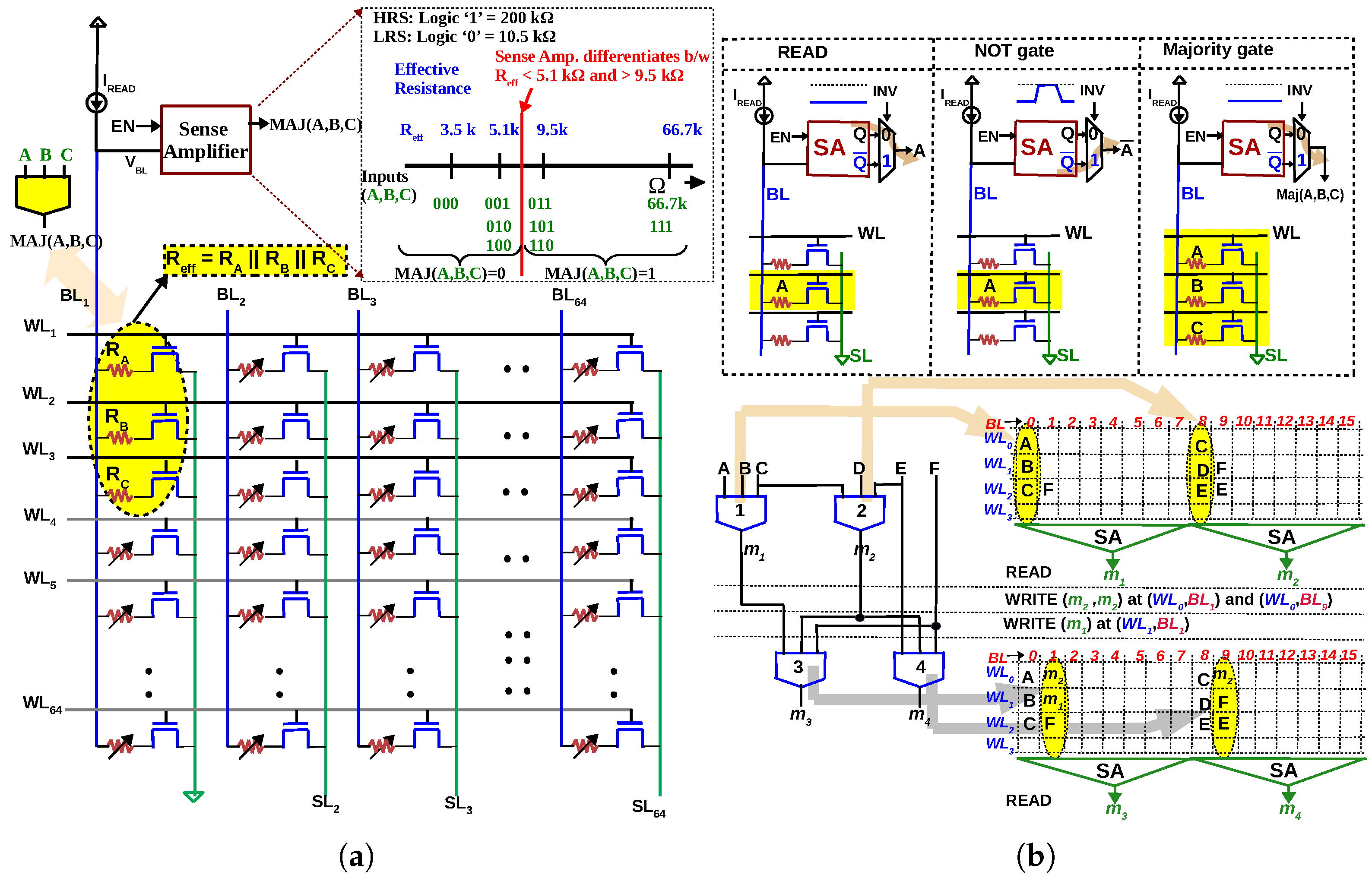
4.1. In-Memory Majority Gate

Before their implementation in memory, the PP adders must first be synthesized in terms of logic gates which can be implemented in memory. As stated, different logic primitives require different modifications to the memory array or its peripheral circuitry (or both). Therefore, for the in-memory implementation of adders, it is important to minimize the different types of logic primitives used. Consequently, it is beneficial to express the adder using one logic primitive, rather than four different logic primitives. Recently, an in-memory majority gate was proposed in [31,32]. The three inputs to the majority gate are the three resistances of the memory cells, and the output majority is computed as a READ operation (Figure 3a). This majority gate does not necessitate any major modifications to the peripheral circuitry of a regular memory array, and is also energy-efficient (access transistor for each memory cell minimizes sneak currents, thus lowering energy consumption when compared to other adders implemented in 1S–1R configuration). As depicted in Figure 3b, multiple majority gates can be executed in array columns, which suits PP adders with a similar structure.

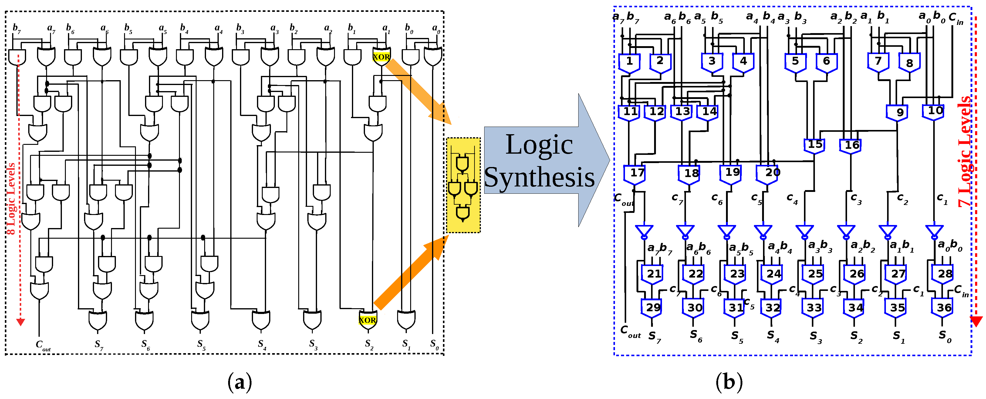
4.2. Homogeneous Synthesis of Parallel-Prefix Adders

Conventionally, PP adders are synthesized in terms of AND, OR and XOR gates for CMOS implementation. Figure 4a depicts an eight-bit PP adder of the Ladner–Fischer type. Three different logic primitives are required—AND, OR and XOR. As stated, different logic primitives require different modifications to the memory array and its peripheral circuitry. If a particular Boolean logic gate cannot be implemented in the memory array, it has to be re-formulated in terms of a logic gate that can be implemented in the memory array. For example, in the NAND-based logic family reported in [10], the XOR gate cannot be implemented; therefore, it is expressed as four NAND gates. As depicted in Figure 4a, a single XOR becomes three levels of NAND logic, increasing its latency. In contrast, by expressing a PP adder purely in terms of MAJORITY+NOT gates, the PP adder can be efficiently implemented in the memory array. Furthermore, a majority-based PP adder achieves a marginal reduction in logical depth compared to conventional AND-OR-XOR implementation (Figure 4). This is due to the majority being a stronger logic primitive than NAND/NOR/IMPLY [13]. To synthesize PP adders in terms of majority gates, logic synthesis tools can be used. A logic synthesis tool is proposed in [8], which takes any AND-OR-INVERT-based logic and synthesizes it purely in terms of majority and NOT gates. Boolean logic minimization techniques such as re-shaping, push-up, node merging, etc., are used to re-synthesize and optimize conventional AND-OR-INVERT logic in terms of MAJORITY-INVERT [33,34,35,36,37,38]. Since the majority is the fundamental logic primitive for many emerging nanotechnologies, there are also works which pioneered the synthesis of PP adders solely in terms of majority gates. The reader is referred to [5,30,39] for such works. Therefore, a variety of techniques can be used to transform PP adders in terms of majority and NOT gates. Figure 4b depicts a 8-bit PP adder, synthesized solely in terms of majority and NOT gates. In addition to achieving homogeneity, the majority-based PP adder incurs one level of reduction in logical depth compared to the AND-OR-XOR-based PP adder.

4.3. Mapping Methodology

Having synthesized the PP adder in terms of majority and NOT gates, they can be implemented in memory using the in-memory majority gate described in Section 4.1. The NOT gate can be implemented as a simple READ operation with the output inverted. The design of in-memory PP adders presented in this paper is generic and can be used to implement any PP adder. However, in this section, the Ladner–Fischer adder of Figure 4b is chosen and the in-memory implementation (mapping) steps are elaborated.

4.3.1. In-Memory Mapping as an Optimization Problem: Objectives

The mapping of the majority-based PP adder to the memory array can be treated as an optimization problem. Any optimization problem has objectives or goals, which should be achieved in the presence of certain constraints. The objectives of in-memory mapping are as follows:
  • Latency of in-memory PP adder must be minimized ( O 1 );
  • Energy consumption during addition must be minimized ( O 2 );
  • Area of the array used during computation must be minimized ( O 3 ).
The aforementioned objectives are no different from the objectives of any VLSI circuit. All objectives cannot be met simultaneously in this mapping, and trade-offs must be made between latency of addition ( O 1 ) and the area of array that is used ( O 3 ). Any arithmetic circuit implemented in memory is bound to be very slow due to the high latency of in-memory adders. The latency of in-memory adders reported in the literature grows, as O ( n ) and 32-bit/64-bit in memory require hundreds of cycles [9]. Therefore, in this mapping, we focus on and minimize the latency. Minimizing the latency might result in the array area being compromised. However, latency is the more serious issue compared to array area in in-memory addition, for the following reasons:
  • A conventional adder (in CMOS) is devoted to addition while we re-use the existing memory array in in-memory computation. Hence, the increased array area required during addition is not a disadvantage, as long as computation can be performed in the memory array without an extra array;
  • ReRAM memory cell or memristor is a nano-device and does not significantly contribute. For example, a single 1T-1R cell in 130 nm CMOS occupies 0.2 μm2 [40].
A significant portion of the energy consumed during in-memory addition is dissipated in the memory array. This is predominantly due to sneak-currents in the 1S–1R array. In contrast, our proposed PP adder is implemented in a transistor-accessed memory array (1T–1R); therefore, the energy dissipation in the array is negligible. The major energy consumption is the energy consumed while the cells switch states (WRITE) and the majority operation (READ). Therefore, the energy consumed during addition is minimized if latency is minimized. In other words, latency ( O 1 ) is the most important objective to be minimized.

4.3.2. In-Memory Mapping as an Optimization Problem: Constraints

The constraints are specific to this design methodology and can be summarized as follows:
  • Majority operation must be executed at three consecutive rows ( C 1 );
  • Due to the bounded endurance of ReRAM devices, the number of times a cell is switched must be minimized. ( C 2 ).
C 1 must be satisfied during mapping because, during majority operation, three rows must simultaneously be selected. In principle, the three selected rows need not be contiguous and can be in different locations in the memory array (e.g., row 5, 8, 15 of a 64 × 64 array). However, row-decoding will become complicated. For practical in-memory implementation, the mapping must be ‘peripheral circuit friendly’. In [32], a triple-row decoder is proposed for triple row-activation during majority operation. To implement this decoder, multiple single-row decoders were interleaved. Furthermore, the same row-decoder must be able to perform single-row decoding and triple-row decoding. This is because, during normal memory operation, a single row must be selected and, during majority, three rows must be selected. To this end, an address translator circuit is used in the row decoder, which seamlessly switches between single-row activation and triple-row activation. The triple-row decoder [32] is designed in such a way that only three consecutive rows can be selected. Therefore, while mapping, the inputs of the majority gate (to be executed in memory in the next step) must be written in three consecutive rows.
Constraint C 2 is posed by a characteristic of non-volatile memories called endurance. A memory device’s endurance refers to its ability to switch between two stable states while maintaining a sufficient resistance ratio. Experimentally reported endurances vary from 106 to 1012. Due to this limited endurance, the number of times a memory cell is switched during addition must be minimized.

4.3.3. Algorithm

Having identified the objectives and constraints, we formulate a generic methodology to map any PP adder to the memory array. As stated, if the PP adder is available in terms of AND-OR-XOR gates, they must be re-synthesized in terms of the majority and NOT gates using logic synthesis techniques/tools. Given a majority-based PP adder, optimal in-memory implementation is an optimization problem—minimize O 1 , while meeting C 1 and C 2 .
The following steps implement the PP adder in the memory:
  • Start with Logic level 1;
  • Simultaneously execute all majority gates of a logic level in the columns of the array ( O 1 );
  • Write the outputs of the majority gates to the precise locations where they are needed in the next logic level such that all the majority gates of the following level can be executed simultaneously ( O 1 );
  • During Step 3, write the outputs of the majority gates to a new location and do not overwrite the existing data ( C 2 );
  • During Step 3, write the outputs of the majority gates to contiguous locations in the memory array ( C 1 );
  • Repeat Steps 2–5 for the remaining logic levels.
Figure 5 illustrates the mapping of an 8-bit PP adder to the memory array. Majority gates 1–8 of the first logic level are executed simultaneously in one memory cycle. Since we know that, at the next level, majority gates 9, 10, 11, 12, 13, 14 need to be executed, we write the outputs of the first logic level ( m 1 , m 2 , m 3 , m 4 , m 5 , m 6 , m 7 , m 8 ) to the exact location where they will be needed. When we write the output of the majority gates back to the array, they are written in consecutive rows ( C 1 ) and are not overwritten on existing data ( C 2 ). The in-memory steps are highlighted in yellow in Figure 5. The in-memory steps corresponding to logic levels 1 and 2 are:
  • Majority at col. (1, 9, 26, 33, 42, 49, 58, 65) rows 4–6 as a READ operation;
  • Write ( m 1 m 1 m 3 m 5 m 7 ) at col. (2, 10, 34, 50, 59), row 4;
  • Write ( m 2 m 2 m 4 m 6 m 8 ) at col. (2, 10, 34, 50, 59), row 5;
  • Write ( m 3 m 4 m 3 m 4 ) at col. (2, 10, 17, 25), row 6;
  • Majority at col. (2, 10, 17, 25, 59, 73) rows 4–6 as a READ operation.
  • ………
In this manner, the seven logic levels of an 8-bit adder can be executed in memory in 18 cycles. A detailed mapping of all seven logic levels is presented in Appendix A.

5. Performance of In-Memory Parallel-Prefix Adders

5.1. Simulation Methodology

To verify the proposed in-memory adder through simulation, the 1T-1R memory array and its peripheral circuitry were designed in IHP’s 130 nm CMOS process. The memory array was composed of 1T-1R cells in which the ReRAM is modelled using the Stanford-PKU model with a 130 nm NMOS transistor as access transistor. A time-based sense amplifier [9] was used to read from the array (majority operation) and an op-amp was used to simultaneously write multiple bits into the array. A triple-row decoder was designed by interleaving multiple single-row decoders. Detailed schematics of the peripheral circuitry are given in [9]. A simultaneous reading (majority operations) and writing across columns of the array was verified by simulation. As described in Section 4.3.3, the adder can be executed in memory as a sequence of READ (majority) and WRITE operations, which are orchestrated by the memory controller (the memory controller can be designed as a finite-state machine and was not designed in this work).

5.2. Latency of In-Memory PP Adders with Increasing Bit-Width

The latency of PP adders grows as log(n). From Figure 6, one can observe that, from 8-bit to 16-bit, the number of logic levels increased by only a single level, i.e., from seven levels to eight levels. The major advantage of the PP adder lies in this ( O ( l o g ( n ) ) logic levels), and we aim to extend this advantage to our in-memory implementation. For the 16-bit version, we have to add an extra level of logic to the carry-generate block to calculate the carry (sum generate block remains at three logic levels; see Figure 6). In general, the number of logic levels, l is given by
l = l o g 2 n + 4
for the n-bit PP adder (Ladner–Fischer type) synthesized in majority logic [30]. When this 16-bit adder was mapped to the memory array following the procedure used for an 8-bit adder (Section 4.3.3), 22 cycles were incurred. As a result of the interconnections between logic levels, the number of in-memory cycles is always higher than the number of logic levels. For an 8-bit adder (Figure A1), a careful comparison of the in-memory cycles indicated that every logic level is translated into at least two cycles, i.e., 2l in-memory cycles. The first few logic levels of the carry–generate block required two more WRITE cycles in addition to the aforementioned WRITE cycles. This additional requirement applies for ( l 5 ) of the l levels. Consequently, the number of cycles required for l logic levels of an n-bit PP adder can be calculated as follows:
C y c l e s i n m e m o r y = ( 2 l ) + 2 ( l 5 ) = 4 l 10 = 4 ( l o g 2 n + 4 ) 10 = 4 · l o g 2 n + 6
Therefore, any PP adder can be implemented in O ( l o g 2 n ) cycles, which is the fastest in-memory adder reported to date (a detailed comparison is given in Section 5.5).

5.3. Energy of In-Memory PP Adders with Increasing Bit-Width

The energy consumed during in-memory addition is composed of the actual energy consumed due to addition (switching ReRAM cells during writing; energy consumed in the SA during majority operation) and the array leakage energy. The array leakage energy is the inherent energy consumption due to sneak currents in transistor-less arrays (e.g., some works, such as [41], used a diode to suppress these sneak currents). However, the proposed adder is executed in a 1T–1R array where the sneak currents are negligible. Hence, array leakage energy can be neglected. The energy used to write into an ReRAM cell is E W R I T E ≈ 12 pJ/bit for IHP’s ReRAM. The energy used for majority operation is the energy consumed in the SA, and is given by, E M A J ≈ 0.63 pJ/majority operation. As can be seen in Figure A1, during eight-bit addition, there are 36 majority operations; 8 NOT and 85 bits are written to the array. Neglecting the energy of an NOT operation (which is only 0.13 pJ/bit), the energy needed for eight-bit in-memory addition is
E n e r g y 8 b i t = 36 × E M A J + 84 × E W R I T E
Observing that E W R I T E is 20 × E M A J , the in-memory addition energy is dominated by the energy that is needed to write into the array.
E n e r g y 8 b i t 84 × E W R I T E
where E W R I T E is the energy that is needed to write to a single bit. Similarly, during 16-bit addition in memory, 180 cells are written [9]. In general, for n-bit addition, (2 n 2 ) × 6 cells are written, making the energy for n-bit addition,
E n e r g y n b i t ( 2 n 2 ) × 6 × E W R I T E
To summarize, the energy for the proposed in-memory adder grows as 12 n times the WRITE energy/bit.

5.4. Area of In-Memory PP Adders with Increasing Bit-Width

In all in-memory adders, the peripheral circuitry of the array is modified to support logic operations, resulting in an increase in the CMOS peripheral circuit area. This increase is a significant factor to consider, since this increase in the silicon area is used solely to make the array ‘computable’. Therefore, a holistic comparison between in-memory adders should consider both the increase in the peripheral circuitry area and the array area (occupied during addition), with the former being the more significant factor. In this work, the triple-row decoder is the only change required, while all other parts of the peripheral circuitry do not change, since computation is performed using normal memory operations (READ and WRITE). The array area used during the addition is simple to calculate—only six rows are needed, independent of the adder size (see Figure A1). In the of Figure A1 mapping, it is assumed that eight columns share a sense amplifier (this is the case when considering pitch-matching, although there are works which assume a sense amplifier for each column). For 8-bit addition, 80 columns are needed, and for n-bit addition, 8n + 16 columns are needed. Therefore, for n-bit addition, the required array area is 6 × (8n + 16).

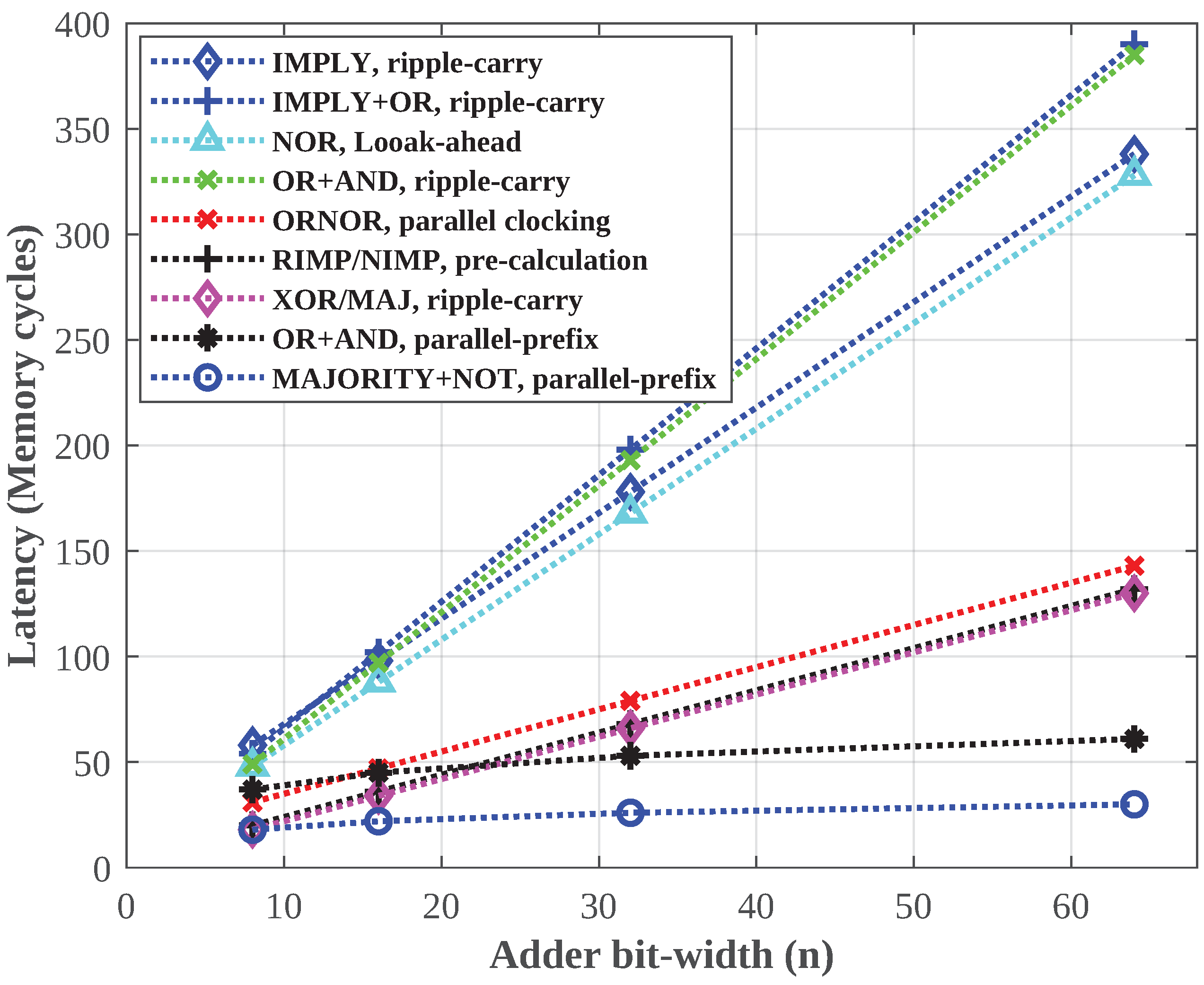
5.5. Comparison with Other In-Memory Adders

In this section, we compare the presented in-memory PP adder design methodology with other adders and evaluate the latency with increasing bit-width. In Table 2, the latency of the proposed in-memory PP adder is compared with the latency of in-memory adders summarized in Table 1. With the exception of the two PP adders, the latency of all other adders is O ( n ) . The sklansky PP adder of [15] incurs a delay of 8 l o g 2 ( n ) + 13, while the majority-based PP adder presented in this work incurs a latency of 4 l o g 2 ( n ) + 6. With a PP architecture, majority logic-based implementation outperforms the OR/AND implementation of [15] in terms of latency. This proves that majority is a stronger logic primitive than OR/AND. The issue of latency becomes more evident when we observe the latency for increasing bit-width. For an 8-bit addition, the XOR-based ripple-carry adders [23,24] incur a latency of 18, which is the same latency as that incurred by the majority-based PP adder. A superficial observation may lead one to conclude that logic primitive alone plays a key role, and both XOR and MAJ are equally good, irrespective of the architecture used. However, the latency of XOR-based adders [23,24] grows to 2n + 2, while that of majority-based PP adder grows to 4 l o g 2 ( n ) + 6. In other words, for a 32-bit addition, the XOR-based adders incurs 66 cycles, while the proposed majority-based PP adder will incur only 26 cycles. This disparity further increases for 64-bit additions. In Figure 7, the latency of in-memory adders is plotted for increasing bit-width to better visualize this trend. As plotted in Figure 7, the proposed adder is one of the in-memory adders with the least latency, since it logarithmically depends on n. This latency advantage is obtained with only a minor modification to the row-decoder of a conventional memory. It must be noted that most other in-memory adders, compared in Table 2, require significant modifications to the peripheral circuitry. The energy consumption of the proposed in-memory adder is mainly due to the HRS ↔ LRS switching energy of the cells during addition. The leakage energy, due to sneak-path currents (which constitutes a significant portion of the total addition energy in 1S–1R adders), is avoided by the access transistor.

6. Conclusions

The latency of in-memory adders is a severe disadvantage in in-memory computing, i.e., any adder is implemented in the memory array as a long sequence of Boolean operations. A poorly optimized in-memory adder may take longer to compute than the combined time it takes to fetch data from memory and compute in a CMOS processor. In-memory adders have not had their latency analyzed and optimized for higher bit-width, and consequently incur O ( n ) latency for n-bit addition (32-bit/64-bit adders, typically used in microprocessors, will require hundreds of cycles). In this work, a design methodology is presented to tackle the exorbitant latency of in-memory adders. The strength of the majority logic primitive is coupled with the parallel-prefix (PP) adder architecture to achieve a latency of 4 l o g 2 ( n ) +6 for parallel-prefix additions in the memory array. The main contribution of this work is a generic mapping methodology, used to map a parallel-prefix adder circuit (synthesized in majority logic) to the memory array with minimum latency. Multiple majority operations can be performed simultaneously in the columns of the array, and could achieve a O ( l o g ( n ) ) latency for any PP adder. Using the proposed design methodology, 32-bit and 64-bit adders (used in processors) can be implemented in 26 and 30 memory cycles, respectively. This can pave the way for arithmetic and similar computing tasks to be efficiently performed at the data location.

Funding

This research received no external funding.

Institutional Review Board Statement

Not applicable.

Informed Consent Statement

Not applicable.

Data Availability Statement

Not applicable.

Conflicts of Interest

The author declares no conflict of interest.

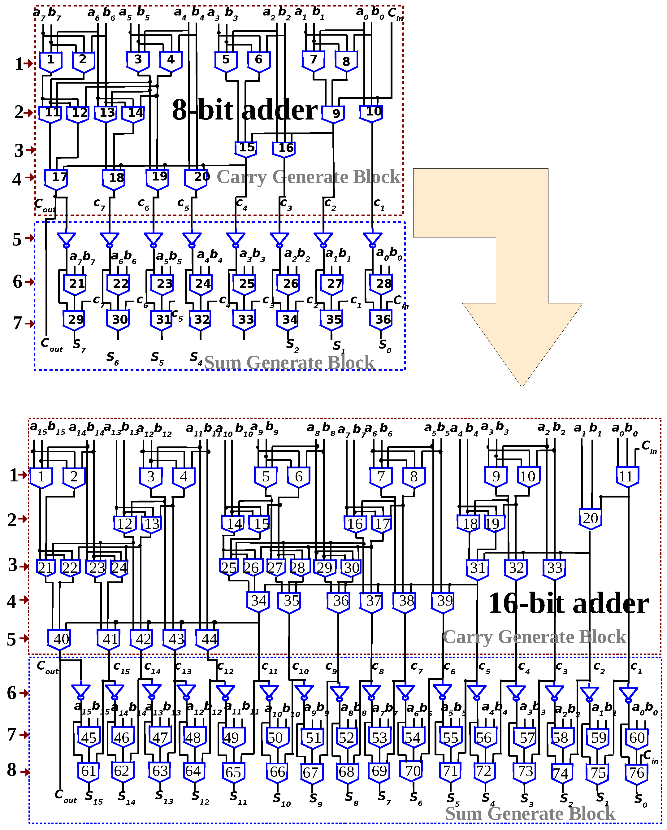
Appendix A. Mapping of 8-Bit Ladner-Fischer Adder to Memory Array

Figure A1. Mapping of the eight-bit LF adder of Figure 5 to memory array. All the majority gates in a level are simultaneously executed (red boxes). During parallel-prefix addition, m i represents the output of the ith majority gate, and c i is the carry (denoted in green color, since it is read as a voltage before being written into the array). 3 WRITE denotes writing cycles to 3 different rows, where more than 1 bit may be written in each row.
Jlpea 11 00045 g0a1

References

  1. Horowitz, M. Computing’s energy problem (and what we can do about it). In Proceedings of the 2014 IEEE International Solid-State Circuits Conference Digest of Technical Papers (ISSCC), San Francisco, CA, USA, 9–13 February 2014; pp. 10–14. [Google Scholar] [CrossRef]
  2. Pedram, A.; Richardson, S.; Horowitz, M.; Galal, S.; Kvatinsky, S. Dark Memory and Accelerator-Rich System Optimization in the Dark Silicon Era. IEEE Des. Test 2017, 34, 39–50. [Google Scholar] [CrossRef] [Green Version]
  3. Singh, G.; Chelini, L.; Corda, S.; Awan, A.J.; Stuijk, S.; Jordans, R.; Corporaal, H.; Boonstra, A. A Review of Near-Memory Computing Architectures: Opportunities and Challenges. In Proceedings of the 2018 21st Euromicro Conference on Digital System Design (DSD), Prague, Czech Republic, 29–31 August 2018; pp. 608–617. [Google Scholar]
  4. Sebastian, A.; Le Gallo, M.; Khaddam-Aljameh, R.; Eleftheriou, E. Memory devices and applications for in-memory computing. Nat. Nanotechnol. 2020, 15, 529–544. [Google Scholar] [CrossRef] [PubMed]
  5. Jaberipur, G.; Parhami, B.; Abedi, D. Adapting Computer Arithmetic Structures to Sustainable Supercomputing in Low-Power, Majority-Logic Nanotechnologies. IEEE Trans. Sustain. Comput. 2018, 3, 262–273. [Google Scholar] [CrossRef]
  6. Ziegler, M.; Stan, M. A unified design space for regular parallel prefix adders. In Proceedings of the Proceedings Design, Automation and Test in Europe Conference and Exhibition, Paris, France, 16–20 February 2004; Volume 2, pp. 1386–1387. [Google Scholar] [CrossRef]
  7. Kvatinsky, S.; Satat, G.; Wald, N.; Friedman, E.G.; Kolodny, A.; Weiser, U.C. Memristor-Based Material Implication (IMPLY) Logic: Design Principles and Methodologies. IEEE Trans. Very Large Scale Integr. (VLSI) Syst. 2014, 22, 2054–2066. [Google Scholar] [CrossRef]
  8. Amarú, L.; Gaillardon, P.E.; Micheli, G.D. Majority-Inverter Graph: A New Paradigm for Logic Optimization. IEEE Trans. Comput.-Aided Des. Integr. Circuits Syst. 2016, 35, 806–819. [Google Scholar] [CrossRef] [Green Version]
  9. Reuben, J.; Pechmann, S. Accelerated Addition in Resistive RAM Array Using Parallel-Friendly Majority Gates. IEEE Trans. Very Large Scale Integr. (VLSI) Syst. 2021, 29, 1108–1121. [Google Scholar] [CrossRef]
  10. Shen, W.; Huang, P.; Fan, M.; Han, R.; Zhou, Z.; Gao, B.; Wu, H.; Qian, H.; Liu, L.; Liu, X.; et al. Stateful Logic Operations in One-Transistor-One- Resistor Resistive Random Access Memory Array. IEEE Electron Device Lett. 2019, 40, 1538–1541. [Google Scholar] [CrossRef]
  11. Ben-Hur, R.; Ronen, R.; Haj-Ali, A.; Bhattacharjee, D.; Eliahu, A.; Peled, N.; Kvatinsky, S. SIMPLER MAGIC: Synthesis and Mapping of In-Memory Logic Executed in a Single Row to Improve Throughput. IEEE Trans. Comput.-Aided Des. Integr. Circuits Syst. 2019, 39, 2434–2447. [Google Scholar] [CrossRef]
  12. Adam, G.C.; Hoskins, B.D.; Prezioso, M.; Strukov, D.B. Optimized stateful material implication logic for three- dimensional data manipulation. Nano Res. 2016, 9, 3914–3923. [Google Scholar] [CrossRef]
  13. Reuben, J. Rediscovering Majority Logic in the Post-CMOS Era: A Perspective from In-Memory Computing. J. Low Power Electron. Appl. 2020, 10, 28. [Google Scholar] [CrossRef]
  14. Ali, K.A.; Rizk, M.; Baghdadi, A.; Diguet, J.P.; Jomaah, J.; Onizawa, N.; Hanyu, T. Memristive Computational Memory Using Memristor Overwrite Logic (MOL). IEEE Trans. Very Large Scale Integr. (VLSI) Syst. 2020, 28, 2370–2382. [Google Scholar] [CrossRef]
  15. Siemon, A.; Menzel, S.; Bhattacharjee, D.; Waser, R.; Chattopadhyay, A.; Linn, E. Sklansky tree adder realization in 1S1R resistive switching memory architecture. Eur. Phys. J. Spec. Top. 2019, 228, 2269–2285. [Google Scholar] [CrossRef]
  16. Karimi, A.; Rezai, A. Novel design for a memristor-based full adder using a new IMPLY logic approach. J. Comput. Electron. 2018, 17, 11303–11314. [Google Scholar] [CrossRef]
  17. Cheng, L.; Li, Y.; Yin, K.-S.; Hu, S.-Y.; Su, Y.-T.; Jin, M.-M.; Wang, Z.-R.; Chang, T.-C.; Miao, X.-S. Functional Demonstration of a Memristive Arithmetic Logic Unit (MemALU) for In-Memory Computing. Adv. Funct. Mater. 2019, 29, 1905660. [Google Scholar] [CrossRef]
  18. Ganjeheizadeh Rohani, S.; Taherinejad, N.; Radakovits, D. A Semiparallel Full-Adder in IMPLY Logic. IEEE Trans. Very Large Scale Integr. (VLSI) Syst. 2020, 28, 297–301. [Google Scholar] [CrossRef]
  19. Talati, N.; Gupta, S.; Mane, P.; Kvatinsky, S. Logic Design Within Memristive Memories Using Memristor-Aided loGIC (MAGIC). IEEE Trans. Nanotechnol. 2016, 15, 635–650. [Google Scholar] [CrossRef]
  20. Kim, Y.S.; Son, M.W.; Song, H.; Park, J.; An, J.; Jeon, J.B.; Kim, G.Y.; Son, S.; Kim, K.M. Stateful In-Memory Logic System and Its Practical Implementation in a TaOx-Based Bipolar-Type Memristive Crossbar Array. Adv. Intell. Syst. 2020, 2, 1900156. [Google Scholar] [CrossRef] [Green Version]
  21. Siemon, A.; Drabinski, R.; Schultis, M.J.; Hu, X.; Linn, E.; Heittmann, A.; Waser, R.; Querlioz, D.; Menzel, S.; Friedman, J.S. Stateful Three-Input Logic with Memristive Switches. Sci. Rep. 2019, 9, 14618. [Google Scholar] [CrossRef] [PubMed] [Green Version]
  22. Siemon, A.; Menzel, S.; Waser, R.; Linn, E. A Complementary Resistive Switch-Based Crossbar Array Adder. IEEE J. Emerg. Sel. Top. Circuits Syst. 2015, 5, 64–74. [Google Scholar] [CrossRef] [Green Version]
  23. TaheriNejad, N. SIXOR: Single-Cycle In-Memristor XOR. IEEE Trans. Very Large Scale Integr. (VLSI) Syst. 2021, 29, 925–935. [Google Scholar] [CrossRef]
  24. Pinto, F.; Vourkas, I. Robust Circuit and System Design for General-Purpose Computational Resistive Memories. Electronics 2021, 10, 1074. [Google Scholar] [CrossRef]
  25. Wang, Z.-R.; Li, Y.; Su, Y.-T.; Zhou, Y.-X.; Cheng, L.; Chang, T.-C.; Xue, K.-H.; Sze, S.M.; Miao, X.-S. Efficient Implementation of Boolean and Full-Adder Functions With 1T1R RRAMs for Beyond Von Neumann In-Memory Computing. IEEE Trans. Electron Devices 2018, 65, 4659–4666. [Google Scholar] [CrossRef]
  26. Dimitrakopoulos, G.; Papachatzopoulos, K.; Paliouras, V. Sum Propagate Adders. IEEE Trans. Emerg. Top. Comput. 2021, 9, 1479–1488. [Google Scholar] [CrossRef]
  27. Knowles, S. A family of adders. In Proceedings of the 15th IEEE Symposium on Computer Arithmetic. ARITH-15 2001, Vail, CO, USA, 11–13 June 2001; pp. 277–281. [Google Scholar] [CrossRef]
  28. Dimitrakopoulos, G.; Nikolos, D. High-speed parallel-prefix VLSI Ling adders. IEEE Trans. Comput. 2005, 54, 225–231. [Google Scholar] [CrossRef]
  29. Harris, D. A taxonomy of parallel prefix networks. In The Thirty-Seventh Asilomar Conference on Signals, Systems Computers; IEEE: Pacific Grove, CA, USA, 2003; pp. 2213–2217. [Google Scholar] [CrossRef]
  30. Pudi, V.; Sridharan, K.; Lombardi, F. Majority Logic Formulations for Parallel Adder Designs at Reduced Delay and Circuit Complexity. IEEE Trans. Comput. 2017, 66, 1824–1830. [Google Scholar] [CrossRef]
  31. Reuben, J. Binary Addition in Resistance Switching Memory Array by Sensing Majority. Micromachines 2020, 11, 496. [Google Scholar] [CrossRef]
  32. Reuben, J.; Pechmann, S. A Parallel-friendly Majority Gate to Accelerate In-memory Computation. In Proceedings of the 2020 IEEE 31st International Conference on Application-Specific Systems, Architectures and Processors (ASAP), Manchester, UK, 6–8 July 2020; pp. 93–100. [Google Scholar]
  33. Wang, P.; Niamat, M.Y.; Vemuru, S.R.; Alam, M.; Killian, T. Synthesis of Majority/Minority Logic Networks. IEEE Trans. Nanotechnol. 2015, 14, 473–483. [Google Scholar] [CrossRef]
  34. Chung, C.C.; Chen, Y.C.; Wang, C.Y.; Wu, C.C. Majority logic circuits optimisation by node merging. In Proceedings of the 2017 22nd Asia and South Pacific Design Automation Conference (ASP-DAC), Chiba, Japan, 16–19 January 2017; pp. 714–719. [Google Scholar] [CrossRef]
  35. Riener, H.; Testa, E.; Amaru, L.; Soeken, M.; Micheli, G.D. Size Optimization of MIGs with an Application to QCA and STMG Technologies. In Proceedings of the 2018 IEEE/ACM International Symposium on Nanoscale Architectures (NANOARCH), Athens, Greece, 17–19 July 2018; pp. 1–6. [Google Scholar]
  36. Devadoss, R.; Paul, K.; Balakrishnan, M. Majority Logic: Prime Implicants and n-Input Majority Term Equivalence. In Proceedings of the 2019 32nd International Conference on VLSI Design and 2019 18th International Conference on Embedded Systems (VLSID), Delhi, India, 5–9 January 2019; pp. 464–469. [Google Scholar] [CrossRef]
  37. Neutzling, A.; Marranghello, F.S.; Matos, J.M.; Reis, A.; Ribas, R.P. maj-n Logic Synthesis for Emerging Technology. IEEE Trans. Comput.-Aided Des. Integr. Circuits Syst. 2020, 39, 747–751. [Google Scholar] [CrossRef]
  38. Kaneko, M. A Novel Framework for Procedural Construction of Parallel Prefix Adders. In Proceedings of the 2019 IEEE International Symposium on Circuits and Systems (ISCAS), Sapporo, Japan, 26–29 May 2019; pp. 1–5. [Google Scholar] [CrossRef]
  39. Ayala, C.L.; Takeuchi, N.; Yamanashi, Y.; Ortlepp, T.; Yoshikawa, N. Majority-Logic-Optimized Parallel Prefix Carry Look-Ahead Adder Families Using Adiabatic Quantum-Flux-Parametron Logic. IEEE Trans. Appl. Supercond. 2017, 27, 1–7. [Google Scholar] [CrossRef]
  40. Levisse, A.; Giraud, B.; Noel, J.; Moreau, M.; Portal, J. RRAM Crossbar Arrays for Storage Class Memory Applications: Throughput and Density Considerations. In Proceedings of the 2018 Conference on Design of Circuits and Integrated Systems (DCIS), Lyon, France, 14–16 November 2018; pp. 1–6. [Google Scholar] [CrossRef] [Green Version]
  41. Chang, Y.F.; Zhou, F.; Fowler, B.W.; Chen, Y.C.; Hsieh, C.C.; Guckert, L.; Swartzlander, E.E.; Lee, J.C. Memcomputing (Memristor + Computing) in Intrinsic SiOx-Based Resistive Switching Memory: Arithmetic Operations for Logic Applications. IEEE Trans. Electron Devices 2017, 64, 2977–2983. [Google Scholar] [CrossRef]
Figure 1. (a) An in-memory logic gate (adder) is stateful if its only state variable is resistance. Non-stateful logic gates (adder) also use voltage in conjunction with resistance. (b) In-memory adder implementation favors homogeneity of logic primitives; 1-bit full adder in terms of NOR gates [11], NAND gates [12] and majority gates [13]; (c) Different carry-propagation techniques result in different adder architectures.
Jlpea 11 00045 g001
Figure 2. Generic Structure of PP adders: A ‘carry-generate block’ calculates carry by prefix computation and is then followed by a ‘sum-generate block’ ([30]).
Jlpea 11 00045 g002
Figure 3. (a) In-memory Implementation of majority gate [31,32]: In a 1T-1R array, the resistances ( R A , R B , R C ) in the three rows will be parallel if three rows are selected at the same time. (Inputs of the majority gate A , B , C are represented as resistances R A , R B , R C ). During READ, the effective resistance R e f f can accurately be sensed to implement an in-memory majority gate. (b) NOT operation can be implemented by inverting the output of the SA. With a majority and NOT gate implemented as a READ operation, the array can be used to execute multiple levels of logic by writing back the data, simplifying computing to READ and WRITE operations.
Jlpea 11 00045 g003
Figure 4. (a) Eight-bit PP adder of Ladner–Fischer type expressed in terms of AND, OR, XOR gates. (b) Re-synthesized and optimized in terms of MAJORITY and NOT gates [5,30].
Jlpea 11 00045 g004
Figure 5. Illustration of mapping of the first two logic levels to a memory array. Since each majority operation is executed as a READ operation, it can be written to the exact location it is needed at the next logic level while satisfying C 1 and C 2 . In the above mapping, eight columns share a sense amplifier.
Jlpea 11 00045 g005
Figure 6. Eight-bit and 16-bit PP adder (Ladner–Fischer type) expressed in majority logic [5,30]. From 8-bit to 16-bit, the number of logic levels increased from 7 to 8, i.e., O ( l o g ( n ) ) latency in terms of logic levels, before mapping to the memory array.
Jlpea 11 00045 g006
Figure 7. Latency of in-memory adders with increasing bit-width, n. An adder with O ( l o g ( n ) ) latency is required for 32-bit/64-bit addition to harness the power of in-memory computation.
Jlpea 11 00045 g007
Table 1. Latency of recently reported in-memory adders (8-bit and n-bit).
StatefulPrimitiveArchitectureLatency (8 bit)Latency (n-bit)Ref.
YesIMPLYRipple carry585n + 18[7]
YesIMPLYParallel-serial565n + 16[16]
YesIMPLY + ORRipple carry546n + 6[17]
YesIMPLYSemi-parallel13617n[18]
YesNORRipple carry8310n + 3[19]
YesNORLook-Ahead485n + 8[20]
NoOR + ANDRipple carry496n + 1[14]
YesORNORParallel-clocking312n + 15[21]
YesRIMP/NIMP*Pre-calculation202n + 4[22]
YesXORRipple carry182n + 2[23]
NoXOR + MAJRipple carry182n + 2[24]
YesXNOR/XORCarry-Select9[25]
NoOR + ANDParallel-prefix378 l o g 2 ( n ) + 13[15]
In a Complementary Resistive Switch (CRS) adder, RIMP/NIMP* denotes reverse implication and inverse implication.
Table 2. Latency comparison of in-memory adders (8-bit and n-bit).
Logic PrimitiveArchitectureLatency (8 bit)Latency (n-bit)Ref.
IMPLYRipple carry585n + 18[7]
IMPLYParallel-serial565n + 16[16]
IMPLY + ORRipple carry546n + 6[17]
IMPLYSemi-parallel13617n[18]
NORRipple carry8310n + 3[19]
NORLook-Ahead485n + 8[20]
OR + ANDRipple carry496n + 1[14]
ORNORParallel-clocking312n + 15[21]
RIMP/NIMPPre-calculation202n + 4[22]
XORRipple carry182n + 2[23]
XOR + MAJRipple carry182n + 2[24]
XNOR/XORCarry-Select9[25]
OR + ANDParallel-prefix378 l o g 2 ( n ) + 13[15]
Majority + NOTParallel-prefix184 l o g 2 ( n ) + 6This work
Publisher’s Note: MDPI stays neutral with regard to jurisdictional claims in published maps and institutional affiliations.

